ADC Power Supplies
http://www.planetanalog.com/author.asp?section_id=3041&doc_id=563055
Jonathan Harris, Product Applications Engineer, Analog Devices, 6/2/2014
As I thought about where to go with the next blog, I looked over the comments and questions from my previous blogs to see where you as the reader had questions. It seems we have taken a pretty long journey discussing the various aspects of noise pertaining to ADCs. It became apparent that it would be a good time to begin looking at interfacing to an ADC through these various ports: power supplies, ground, analog inputs, clock input, and digital I/O. This will obviously intertwine with some of the noise discussion we’ve had, but with a little more practical application in mind. We’ll start by taking a look at the power supply inputs of the ADC, what we typically use to supply power to the ADC, and some of the tradeoffs of the different methods.
Before we discuss how to drive the various supply domains, let’s review the power supply inputs that can typically be found on a high-speed ADC. There is an optional input buffer supply domain (not on all ADCs), an analog supply domain, a digital supply domain, and a driver supply domain.
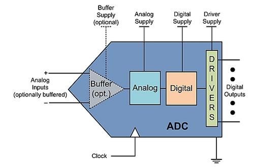
Depending on the ADC, an analog input buffer may be used in front of the ADC analog inputs to the ADC core. In some applications, it can be beneficial to have an input buffer since most high-speed ADCs have a switched capacitor input stage. We won’t dive into a discussion on this topic other than in regard to the power supply requirements when a buffer is present.
Typically, the data conversion (analog section) and digital processing (digital section) are maintained on different supply inputs. The analog section comprises multiple stages of amplifiers, comparators, and other analog circuitry that does most of the analog-to-digital conversion. One could definitely argue that this section isn’t truly purely analog, and one would be correct. Many high-speed converters today have digitally assisted analog sections. But then again, one could also argue that there are no such things as digital circuits since it is all made from analog circuits in the end, but I digress... back to the analog power supply.
Typically the analog supply has its own input for isolation reasons. The same applies to the digital section. There are various portions of circuitry within each of these blocks that operate at different frequencies, and keeping the supply domains separate helps keep these frequencies from making their way back and forth between the two sections. Having crosstalk between these sections can result in degraded performance, which may manifest itself in the SNR (noise performance) or the SFDR (spurious performance) of the ADC.
In a similar manner, the driver supply domain is typically kept separate from the other supply domains of the converter. The output drivers, depending on the particular type, can be a potential pathway for noise into the converter or may potentially be a source of noise. For example, in ADCs with CMOS outputs, large switching transients could create noise and in particular instances could cause performance issues with the ADC. For CML output drivers that are typically used with high-speed serial ADCs that employ JESD204B outputs, it is best to keep a separate domain to ensure an optimal supply condition for the high output data rates that are required (up to 12.5 Gbit/s).
Stay tuned as we continue to look at the power supply inputs of a typical high-speed ADC. Now that we have an understanding of the various domains, we can start looking at strategies for powering them. Do we exclusively use LDOs? There can be some cases where LDOs can be very appropriate to use and others where they may not be the best option. Can we use a DC/DC converter? It depends. Sometimes, DC/DC converters are the most efficient way to translate supply domains down from a high input voltage. Why not use a combination of both? Now, here we may be on to something! Do we need to use one versus the other?
These are some questions we will explore. I hope you are excited to find out the answers. I am looking forward to discussing them!
http://www.planetanalog.com/author.asp?section_id=3041&doc_id=563214
Last month, we discussed the various power supply inputs of a typical ADC. These include power supply inputs for optional input buffer circuits, the analog circuits, the digital circuits, and the output driver circuits.
With the sampling speeds of currently available ADCs and the many different voltage and clock domains inside a typical ADC, it is usually recommended to keep separation in the power supply inputs. By keeping the power supply inputs on separate domains, crosstalk between supplies can be minimized, and noise has a much harder time crossing between domains, where it could creep up and cause a problem with ADC performance. If it is not possible to keep them on separate domains, then at a minimum components such as ferrite beads can be used to give some isolation between supply domains. One method of driving the power supply inputs separately is by using low dropout (LDO) voltage regulators. An example is shown in Figure 1 below.

LDOs are typically the safest type of power supply and typically have the least risk in driving the power supply inputs to an ADC. Generally, LDOs offer very low noise and a high power supply rejection ratio (PSRR). The low dropout typically means that the input supply to the LDO can be as low as a few hundred millivolts above the LDO's output voltage. For example, the ADP1741 2A LDO can have as little as a 400 mV headroom (Vin must be 400 mV greater than Vout). For a typical supply rail of 1.8 V that one would encounter on an ADC, this means the efficiency of the LDO would be approximately Vout/Vin = 1.8/2.2 = 81.8%.
This is not inefficient by any means, but as we'll find in my upcoming blogs, there are more efficient devices we can use to drive the ADC power supply inputs. However, the efficiency of these other devices comes with a cost. As I mentioned, two of the main advantages of the LDO are the low noise and high PSRR. Other devices typically trade off noise for efficiency.
For the ADP1741, the output noise between 10 Hz and 100 kHz is typically 65 µVrms at an output voltage of 2.5 V. Let's look at an example of the effects of this contribution. In a 14-bit 250 MSPS ADC with an input full scale of 2.0 Vpp and an SNR of 70 dB, the noise floor is 20 nVrms/rt-Hz. In the first Nyquist zone, the ADC noise will be 223.61 µVrms (20 nVrms/rt-Hz * sqrt(250 MHz/2)). In this case, the ADP1741 output noise is much less than the ADC noise. In addition, the PSRR of the ADC (typically 60 dB) will further reduce the ADP1741 noise from 65 µVrms down to 65 nVrms (65 µVrms X 1 mV/V). This makes it easy to see why an LDO is such a nice option for driving the power supply inputs. It has virtually no impact on the ADC noise.
However, this does come with a price. One distinct disadvantage to using an LDO is the potential power dissipation. For example, let's look at the 14-bit ADC in the example above and assume it is a quad-channel device with a total power dissipation of 2 W, of which 1 W is needed for the AVDD supply. In this example, we are limited on the input supply to the LDO, and we have only a 6 V input available to drive the 1.8V AVDD supply. This means the ADP1741 would be required to dissipate an approximate power of (6 V – 1.8 V)/1800 mA = 2.33 W. This would push the maximum junction temperature (Tj) of the ADP1741 to TA + Pd X Θja = 85°C + (2.33 W X 42°C/W) = 183°C, which exceeds the LDO's maximum rating of 150°C.
This, of course, is an extreme example, but it illustrates the point of needing a low input voltage to the LDO. This can lead to using multiple LDOs to step down the voltage from a higher input supply rail down to a lower input supply rail required by the ADC. This provides a good lead into the next discussion. We'll take a look at this topology where multiple LDOs are used, and we'll examine some of the advantages and disadvantages.
Thus far, we've looked at the various power supply inputs of a typical ADC and one method for driving these inputs with LDOs. In part 1 of this series, we specifically looked at using separate LDOs to drive each power supply input. This method provides the best isolation and, in most cases, the best noise performance. As the math demonstrated in the example in part 1, the noise at the LDO output can be much lower than the ADC noise and thus is not a major factor in the overall noise.
However, there are some disadvantages when driving low input supply voltages, where multiple LDOs may be required. Before we take a look at that, I would like to address a reader comment that I thought deserved some attention. The comment was about having too many LDOs in the previous example (one for each power supply input). An alternative approach is to use a single LDO that would fan out to multiple power supply inputs to the ADC. This approach is shown in the figure below.
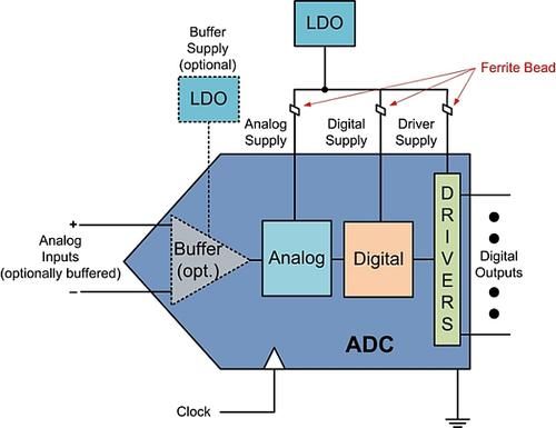
This example moves to the opposite extreme and sources most of the ADC power supply inputs from a single LDO. Let's now look at some of the advantages and disadvantages of this approach and maybe try to examine some middle ground. As you can see from the diagram, this is a rather simple approach that uses fewer components. Reducing the number of LDOs also reduces the overall system cost.
First and foremost, the cost is lower because there is one LDO to purchase, instead of three (in terms of analog, digital, and driver supplies). Secondary to that, with fewer LDOs, there are fewer SMD components for the LDOs: resistors, capacitors, etc. There is cost associated with the new ferrite bead components, but the cost is much less than the cost of the LDO. Currently on the Digi-Key website, the 1.5k unit price for an ADP1741 is $1.53. By contrast, the 1k unit price for a typical ferrite bead on the Digi-Key website is about $0.029. This does not count the savings that can be achieved by using less board space.
This all seems great, doesn't it? If only it were that simple.
This may not be the best solution from a performance standpoint. Care must be taken to select a ferrite bead that provides sufficient isolation without a large DC resistance (DCR). In cases where small supply voltages (1.2 V) are required along with higher input currents (500-1,000 mA), the voltage drop across the ferrite bead could result in performance issues. For example, a ferrite bead with 150 mΩ of DCR on a 1.2V supply requiring 750 mA would have a voltage drop of 150 mΩ × 750 mA = 112.5 mV. That is nearly 10% of the supply voltage. In addition, it may not be possible for one LDO to provide enough current or handle enough power to drive all these power supply inputs.
Let's take another look at the example from part 1, where we calculated the power dissipation in the ADP1741 on the AVDD supply of a typical 14-bit ADC, which required 1 W of power. In that example, the ADC's total power was 2 W. In the same example, if used a total power of 2 W (since we are using a single LDO), the picture wouldn't look as good. The ADP1741 would be required to dissipate an approximate power of (6 V – 1.8 V)*1110 mA = 4.662 W. This would push the maximum junction temperature (Tj) of the ADP1741 to TA + Pd x Θja = 85°C + (4.662 W x 42°C/W) = 281°C, which exceeds the maximum rating for the LDO by over 100 degrees.
(Note: In part 1, the equation for the power should have been (6 V – 1.8 V)*0.5556 = 2.33 W. This was the right power dissipation, but the error was in the presentation of the equation.)
As you can see, there is a balance to be achieved between cost, power, and performance. Does that seem familiar? I think we all face this tradeoff in most of our designs. Next time, we will continue looking at the power supply inputs to the ADC and how we can use multiple LDOs or a combination of LDOs and ferrite beads to mitigate the power dissipation dilemma. This does come with some increased cost, as you can deduce from my comments in this blog, but performance does not come for free, as we all know. I welcome and encourage the comments and questions. There is always time to stop along the way and dive a little further into different areas that interest our community members.
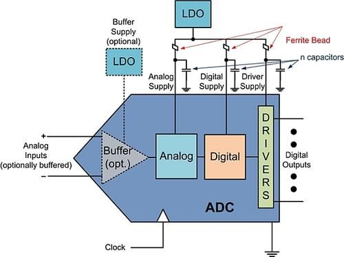
After reading through the comments and having a few discussions with some of my coworkers, I thought it would be good to continue looking at the example I gave in my last blog (Interfacing to ADCs: Power Supplies, Part 2) where we looked using fewer LDOs and combining power supply rails on an ADC while maintaining isolation with ferrite beads. One very important item that I’ve left off thus far has been proper power supply decoupling. The focus has been more at a high level and looking at the topologies that can be used for ADC power supplies.
I want to take a moment to go back to that example and add in the decoupling. The size and value of the decoupling capacitors (shown as n capacitors in Figure 1) will depend on several factors, such as power supply voltage, frequency of operation, ADC power consumption, LDO characteristics, etc. There are many items to look at, but for the purpose of this discussion we will assume that the proper decoupling capacitors have been chosen. I’d ask that the reader keep in mind that it is always good design practice to decouple the power supply inputs to the ADC properly.
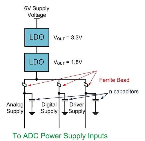
Let’s now take a look at a topology that will mitigate some of the power consumption issues we have looked at in the last few blogs. In many cases there is a higher voltage supply available in the system, but a lower supply voltage is required from the ADC. Many of the ADCs available today use a 1.8V power supply voltage. In many systems a higher supply voltage such as 6V or 12V is available (and could be higher in some cases). Let’s take a look at an example where a 6V power supply voltage is available and the ADC requires a 1.8V power supply input. For the purposes of this discussion we’ll focus mainly on the analog, digital, and driver supply inputs of the ADC. The input buffer supply is often a higher voltage such as 3.3V and is not a high current supply input, so the drop from 6V to 3.3V can be accomplished with a single LDO.
Figure 2

Let’s look at an example using the 14-bit 250MSPS dual channel AD9250. The typical total power consumption listed in the data sheet for the AD9250 is 711mW. This ADC has three power supply inputs which are the analog (AVDD), digital (DVDD), and driver (DRVDD) supplies. Let’s use the topology shown in Figure 1 and calculate the power consumption and junction temperatures. For this example, we will use two ADP1741 LDOs -- one configured for a 3.3V output and the other configured for a 1.8V output -- so that we produce the supply voltage needed as shown in Figure 1.
To begin, let’s look at the total current draw from the AD9250. Summing the current requirements from the three supplies, the total current requirement of the AD9250 is 255mA (IAVDD) + 140mA (IDRVDD + IDVDD) = 395mA. First let’s look at the case for the ADP1741 generating the 3.3V from the 6V supply input. In this case, the ADP1741 will be required to dissipate (6V – 3.3V) x 395mA = 1.067W. The means the maximum junction temperature Tjwould be equal to TA + Pd x Θja = 85oC + 1.067W x 42oC/W = 129.79oC, which is less than the maximum rated junction temperature of 150oC for the ADP1741.
This is the larger of the two voltage drops on the supply rail so it means the second ADP1741 is ok as well, but let’s look at the calculations. We have the same current since the second ADP1741 as in the first ADP1741, which is 395mA. For the case of the second ADP1741, we have a voltage drop of 3.3V – 1.8V = 1.5V. Calculating the power dissipation, we arrive at (3.3V – 1.8V) x 395mA = 0.5925W. Now, calculating the maximum junction temperature we get 85oC + 0.5925W x 42oC/W = 109.89oC, which is once again less than the maximum rated junction temperature of the ADP1741. Assuming we have properly selected the ferrite beads and decoupling capacitors, we have arrived at a nicely functioning power supply for the ADC. Stay tuned as we continue to look at driving ADC power supplies.
have been considering various topics pertaining to ADC power supply inputs over the last several blogs, so let’s continue in that direction and keep expanding on the topic just a bit.
Thus far, we’ve looked at the different types of power supply inputs to an ADC and then a few ways we can drive them. Mainly we have focused on using LDOs, but we have seen this may not always be the best approach. Depending on system constraints and performance specifications, other topologies might be better. In that vein, let us look at using a DC/DC converter (sometimes referred to as a switching regulator) along with an LDO to drive the ADC power supply inputs (see Figure 1).
When using a DC/DC converter it is important to make sure that the output LC filter is properly designed for the current requirements of the design and the switching frequency of the DC/DC converter. It is also important to keep the current return loops in the current switching paths very short and tight around the DC/DC converter. We will keep this part of the discussion high-level and talk a bit about the effects that may show up in the FFT of the digitized data of the ADC.
First let’s look at the power consumption, as we have done in the last few blogs. In this case we will assume a 5.0 V supply rail as an input and that we are using the ADP2114 DC/DC converter and the ADP1741 LDO. In order to calculate the power dissipation of the ADP2114 we can download the ADIsimPower tool for the device. This tool will help us calculate the power dissipated by the ADP2114 as well as generate a schematic and design. For this example, we will only look at the power calculated by the tool.
Let’s again consider the AD9250 where the total current requirement for the device is 395 mA with an input supply voltage of 5.5 V, an output voltage of 2.5V, and the selection for “Most Efficient” design in the tool (see Figure 2 below).
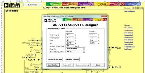
Entering these values into the ADIsimPower tool for the ADP2114, the results are computed, which show an efficiency of 96.4% with a power dissipation of 37 mW. This is quite a bit more efficient than the previous examples we’ve looked at! This is exactly one of the reasons a DC/DC converter can be attractive. Finishing out this example, let’s now calculate the power dissipation in the ADP1741 now that we have a 2.5 V supply voltage available from the ADP2114.
In this case, the ADP1741 will be required to dissipate (2.5 V – 1.8 V) x 395mA = 276.5 mW. The means the maximum junction temperature Tj would be equal to TA + Pd x θ ja = 85oC + 276.5 mW x 42oC/W = 96.61oC, which is considerably less than the maximum rated junction temperature of 150oC for the ADP1741. This is a much better operating condition than in our previous examples. So what is the catch? Well, there are definitely things to consider when using a DC/DC converter. Since the DC/DC converter is a switching device, there are switching transients to be aware of that can manifest as spurs in the ADC output spectrum (see Figure 3).

The placement of the switching of these switching spurs will be dependent upon the switching frequency of the DC/DC converter and the input frequency of the ADC. The switching spurs will mix with the input signal, and spurs will result at fIN – fSW and fIN + fSW. The good news is that, with proper design, the amplitude of these spurs can be minimized and in many cases be lower than the harmonics or other spurs in the ADC spectrum, making them a non-issue. The ADIsimPower tool provides a schematic as well as a recommended layout so that the user can have an optimized design to minimize the effects of the switching action of the DC/DC converter (see Figures 4 and 5).

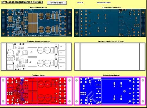
I encourage the use of the ADIsimPower tool. It is quite handy when looking to generate a power supply design for a system. We have used the tool here for an ADC, but the tool’s use is not limited to just ADCs. Stay tuned as we continue to look at ADC power supplies. Thanks again for the great comments and questions -- please keep those coming.
In Interfacing to ADCs: Power Supplies, Part 4, we looked at using a DC/DC converter (switching regulator) in combination with an LDO to drive the power supply inputs to an ADC. What we found was that using the DC/DC converter to step down the input voltage for the LDO was a much more efficient way to drive the power supply inputs to an ADC. As a reminder, this topology is given in Figure 1 below. The input supply voltage is 5.0 V, which is stepped down to 2.5 V and then input to the LDO, which has a 1.8 V output for the ADC supply voltages.
By using proper circuit design with a good filter design on the output of the LDO as given by Figure 3, the switching spurs can be greatly reduced. This by itself is not all that it takes however, it is also important to pay attention to the layout. Just as with any high frequency or switching device, it is important to pay attention to current return paths to make sure there isn’t a potential for the switching noise to make its way into the ADC or other components that may also be on the same board. It is important to keep these current return paths very small. It is also important to keep them physically isolated from sensitive nodes in the design so the switching noise coupling is minimized.
As you can see, there are many aspects to consider, but that is what makes engineering so challenging and fun at the same time. Stay tuned as we look next time at driving the power supply inputs to an ADC directly from a DC/DC converter.
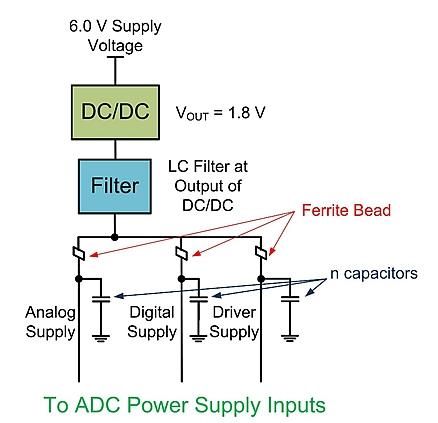
In Interfacing to ADCs: Power Supplies, Part 5 we looked at the switching spurs and the PSRR of an LDO and an ADC when using a DC/DC converter (switching regulator) in combination with an LDO to drive the power supply inputs of the ADC. We have seen in this blog series that this method is more efficient than using just LDOs. In this blog we’ll take this one step further and look at driving the ADC power supplies directly from a DC/DC converter (shown in Figure 1.) The input supply voltage is 6.0 V, which is stepped down to 1.8 V for the ADC supply voltages. I have separately called out the LC filter that resides at the output of the DC/DC converter, as this is especially critical for this design to filter the switching transient spurs generated at the DC/DC converter switching frequency.
Once again, we will look at an example with the AD9683. In this example, we will use the ADP2442 DC/DC converter with 1 A output current capability. This is sufficient for the AD9683, which requires a maximum total current of 263 mA. In order to generate the proper application circuit for the ADP2442 to drive the AD9683 we will once again turn to the ADIsimPower tool, which is available for the ADP2442 at ADP2442 ADIsimPower Tool. The first step is to input the system parameters (shown in Figure 2).

As mentioned above, we are using a 6.0 V supply for the ADP2442 with an output voltage of 1.8V and an output current of 260 mA. I have used the maximum total current draw for the AD9683 and have set the temperature to 85oC since this is the maximum operating temperature. This will make sure that the design will operate up to the typical maximum temperature in most applications. I have chosen for the tool to design the application circuit for the lowest cost. The other available selections are least-part-amount, most-efficient, and smallest-size. I chose lowest-cost because one of the primary drivers in many applications today is for the least expensive solution. With these inputs the tool generates the solution circuit and values given in Figures 3 and 4.
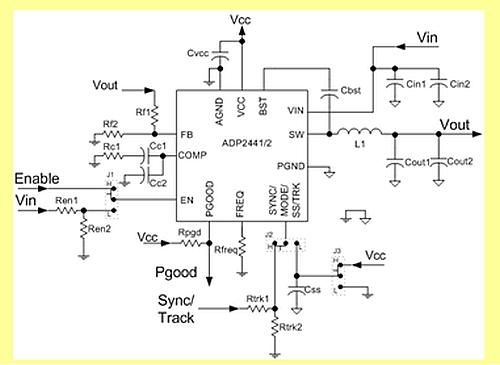
ADP2442/AD9683 Application Circuit Schematic

ADP2442/AD9683 Application Circuit Component Values (Lowest Cost)
The lowest-cost option gives us a total BOM (bill of materials) cost of $2.218. Based on the value of Rfreq we can see that the switching frequency is set to 1 MHz. In this case the efficiency (not pictured but generated by the design tool) is about 75%. The output inductor is a 3.3 µH Coilcraft component, and the output capacitance is a 10 µF Taiyo Yuden component. If we were to choose the option for most-efficient in the design tool, it would yield the BOM shown in Figure 5 below.
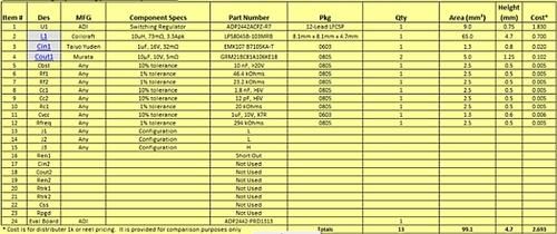
Choosing the most-efficient option yields a total BOM cost of $2.693, which is just a bit more than the previous example. This change results in an increase in the value of the output inductor from 3.3 µH up to 10 µH. As illustrated in the BOM cost, the output inductor is one of the largest cost adders in the system. This is a critical component for a DC/DC converter. The output inductor is typically chosen to have a low DC resistance (DCR), a high self-resonant frequency (SRF), and a high saturation current (ISAT). In addition, the value of Rfreq is different and sets the switching frequency to 314 kHz instead of 1 MHz for the lowest-cost option. In this example, however, the overall efficiency is increased from 75% to 89%. The flexibility of the tool allows the user to choose the best solution for a particular system design.
Using this design tool for ADI power solutions has reminded me that ADI has several software design tools that can be used to prototype a system in advance of a physical design as well as evaluate product performance without hardware. Stay tuned as we take a look at ADIsimADC in the next blog.