Freescale k60的Comparator的操作
The comparator (CMP) module provides a circuit for comparing two analog input voltages. The comparator circuit is designed to operate across the full range of the supply voltage, known as rail-to-rail operation.
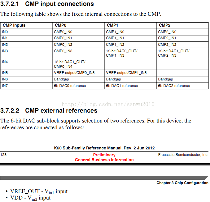
The Analog MUX (ANMUX) provides a circuit for selecting an analog input signal from eight channels. One signal is provided by the 6-bit digital-to-analog converter (DAC).The mux circuit is designed to operate across the full range of the supply voltage.The 6-bit DAC is 64-tap resistor ladder network which provides a selectable voltage reference for applications where voltage reference is needed. The 64-tap resistor ladder network divides the supply reference Vin into 64 voltage levels. A 6-bit digital signal input selects the output voltage level, which varies from Vin to Vin/64. Vin can be selected from two voltage sources, Vin1 and Vin2. The 6-bit DAC from a comparator is vailable as an on-chip internal signal only and is not available externally to a pin。
结构框图
// Configure CMP.
hscmp_clear(); //clear comparator registers
CMP_CR0_REG(cmpch) = 0x00; // Filter and digital hysteresis disabled
CMP_CR1_REG(cmpch) = 0x15; // Continuous mode, high-speed compare, unfiltered output, output pin disabled
CMP_FPR_REG(cmpch) = 0x00; // Filter disabled
CMP_SCR_REG(cmpch) = 0x1E; // Enable rising and falling edge interrupts, clear flags
CMP_DACCR_REG(cmpch) = 0xE0; // 6-bit reference DAC enabled, output set to 1/2-scale, Vdd reference
CMP_MUXCR_REG(cmpch) = 0xC7; // P-input as external channel 0. M-input as 6b DAC
CMP_CR1_REG(cmpch) |= CMP_CR1_OPE_MASK; // Enable output pin for HSCMP0
以上是电子创新网提供的代码中对于CMP的配置部分,我们通过分析这部分代码来对Comparator的使用加以理解。
void hscmp_clear()
{
CMP_MemMapPtr cmpch = CMP0_BASE_PTR;
CMP_CR0_REG(cmpch) = 0;
CMP_CR1_REG(cmpch) = 0;
CMP_FPR_REG(cmpch) = 0;
CMP_SCR_REG(cmpch) = 0x06; // Clear flags if set.
CMP_DACCR_REG(cmpch) = 0;
CMP_MUXCR_REG(cmpch) = 0;
}
(1) CMP_CR0_REG(cmpch) = 0; 将CMP0 Control Register 0 赋值为0,
This makes the filter mode disabled and the hystersis level is Level 0.
(2) CMP_CR1_REG(cmpch) = 0;
SE = 0 means the samlping mode is not selected
WE = 0 means the windowing mode is not selected
PMODE = 0 means the Low-Speed Comprision is selected. In this mode, CMP has slower output propagation(传输) delay and low current consumption.
INV = 0 means the Does not invert(反转) the comparator output
COS = 0 sets the filtered comparator output to equal COUT and COS = 1 sets the unfiltered comparator output to equal COUTA.
OPE = 0 :CMPO is not available on the associated pin .OPE = 1 :CMPO is available on the associated pin .
EN = 0 : The Analog Comparator is disabled. When the user selects the same input from the analog mux to the positive and negetive port, the comparator is disabled automatically.
(3)CMP_FPR_REG(cmpch) = 0;
CMP Filter Peroid Register 这个寄存器在CMP_CR1中的SE位置1 的时候不起任何作用,因为此时外部的采样信号决定了采样的周期,在SE=0的时候,如果FILT_PER = 0,则filter功能disabled。
(4) CMP_SCR_REG(cmpch) = 0x06; // Clear flags if set.
这句换实际上是对位CFR和CFF进行操作,这里需要注意的是CFR和CFF在wirte部分w1c的含义。
CFR is cleared by writing 1 to it and the same as CFF
DMAEN用来使能由CFR和CFF造成的DMA请求,置1表示使能DMA,清零则不使能
IER和IEF用来分别使能由CFR和CFF产生的中断
(5)CMP_DACCR_REG(cmpch) = 0;
以上描述了void hscmp_clear()对于CMP0的配置
CMP_CR0_REG(cmpch) = 0x00; // Filter and digital hysteresis disabled
CMP_CR1_REG(cmpch) = 0x15; // Continuous mode, high-speed compare, unfiltered output, output pin disabled
CMP_FPR_REG(cmpch) = 0x00; // Filter disabled
CMP_SCR_REG(cmpch) = 0x1E; // Enable rising and falling edge interrupts, clear flags
CMP_DACCR_REG(cmpch) = 0xE0; // 6-bit reference DAC enabled, output set to 1/2-scale, Vdd reference
CMP_MUXCR_REG(cmpch) = 0xC7; // P-input as external channel 0. M-input as 6b DAC
CMP_CR1_REG(cmpch) |= CMP_CR1_OPE_MASK; // Enable output pin for HSCMP0
#define CMP_CR1_OPE_MASK 0x2u
因为引脚PTC6的默认功能为CMP0_IN0,因此无需对PTC6进行配置。从引脚PTC6将红外接收管的信号接入Comparator模块中,DAC单元的参考电压选择Vin2,亦即VDD.


