论文阅读-Crossing the abyss: asynchronous signals in a synchronous world
该论文讨论了异步信号的跨时钟域处理问题
Crossing the abyss: asynchronous signals in a synchronous world
Only the most elementary logic circuits use a single clock. Most data-movement applications, including disk-drive controllers, CDROM/DVD controllers, modems, network interfaces, and network processors, bear inherent challenges moving data across multiple clock domains. When signals travel from one clock domain to another, the signal appears to be asynchronous in the new clock domain.
In modern IC, ASIC, and FPGA designs, engineers have many software programs to help them create million-gate circuits, but these programs do not solve the problem of signal synchronization. It is up to the designer to know reliable design techniques that reduce the risk of failure for circuits communicating across clock domains.
Fundamentals
The first step in managing multiclock designs is to understand the problem of signal stability. When a signal crosses a clock domain, it appears to the circuitry in the new clock domain as an asynchronous signal. The circuit that receives this signal needs to synchronize it. Synchronization prevents the metastable state of the first storage element (flip-flop) in the new clock domain from propagating through the circuit.
Metastability is the inability of a flip-flop to arrive at a known state in a specific amount of time. When a flip-flop enters a metastable state, you can predict neither the element's output voltage level nor when the output will settle to a correct voltage level. During this settling time, the flip-flop's output is at some intermediate voltage level or may oscillate and can cascade the invalid output level to flip-flops farther down the signal path.
The input must be stable during a small window of time around the active edge of the clock for any flip-flop. This window of time is a function of the design of the flip-flop, the implementation technology, operating conditions, and the load on the output for outputs that are not buffered. Sharp edge rates on the input signal minimize the window. More windows of vulnerability arise as the clock frequency increases, and the probability of hitting the window increases as the data frequency increases.
FPGA manufacturers and IC foundries qualify their flip-flops and determine their characteristics. “MTBF” (mean time between failures) describes the metastability characteristic of a flip-flop using statistics to determine the probability of a flip-flop's failure. Manufacturers base the MTBF in part on the length of the time window during which a change in the input signal causes the flip-flop to become unstable. In addition, MTBF calculation uses the frequency of the input signal and the frequency of the clock driving the flip-flop.
Each type of flip-flop in an ASIC or FPGA library has timing requirements to help you determine the window of vulnerability. “Setup time” describes the time an input signal to a flip-flop must be stable before the clock edge. “Hold time” is the time the signal must remain stable after the clock edge. These specifications are usually conservative to account for all the possible variations in supply voltage, operating temperature, signal quality, and fabrication. If a design meets these timing requirements, the possibility is negligible that the flip-flop will fail.
Synthesis programs in modern IC and FPGA designs ensure that digital circuits meet the setup-and-hold requirements for each flip-flop in the design; however, asynchronous signals pose problems for the software. A signal crossing a clock domain appears to be asynchronous to the logic in the new clock domain. Most synthesis programs have trouble determining whether asynchronous signals meet the timing requirements for flip-flops. Because they cannot determine the time the flip-flop is unstable, they cannot determine the total delay from the flip-flop through the combinational logic to the next flip-flop. The best course, then, is to use circuits that mitigate the impact of asynchronous signaling.
Signal synchronization
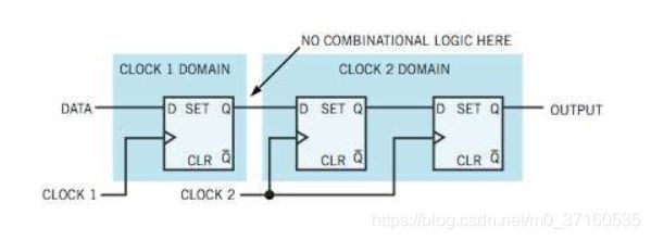
The purpose of synchronizing signals is to protect downstream logic from the metastable state of the first flip-flop in a new clock domain. A simple synchronizer comprises two flip-flops in series without any combinational circuitry between them. This design ensures that the first flip-flop exits its metastable state and its output settles before the second flip-flop samples it. You also need to place the flip-flops close to each other to ensure the smallest possible clock skew between them.
IC foundries help with signal synchronization by providing synchronizer cells. These cells usually comprise a flip-flop with a very high gain that uses more power and is larger than a standard flip-flop. Such a flip-flop has reduced setup-and-hold-time requirements for the input signal and is resistant to oscillation when the input signal causes a metastable condition. Another type of synchronizer cell contains two flip-flops, thus easing your job by placing the flip-flops close to each other and preventing you from placing any combinational logic between them.
For synchronization to work properly, the signal crossing a clock domain should pass from flip-flop in the original clock domain to the first flip-flop of the synchronizer without passing through any combinational logic between the two (Figure 1 ). This requirement is important because the first stage of a synchronizer is sensitive to glitches that combination logic produces. A long enough glitch that occurs at the correct time could meet the setup-and-hold requirements of the first flip-flop in the synchronizer, leading the synchronizer to pass a false-valid indication to the rest of the logic in the new clock domain.
Figure 1 In a full synchronizer circuit, the signal-crossing clock domains should pass from the originating flip-flop in the original clock domain to the first flip-flop of the synchronizer without passing through any combinational logic between the originating flip-flop and the first flip-flop of the synchronizer.
A synchronized signal is valid in the new clock domain after two clock edges. The signal delay is between one and two clock periods in the new clock domain. A rule of thumb is that a synchronizer circuit causes two clock cycles of delay in the new clock domain, and a designer needs to consider how synchronization delay impacts timing of signals crossing clock domains.
There are many designs for synchronizers because one type does not work well in all applications. Synchronizers fall into one of three basic categories: level, edge-detecting, and pulse (Table 1 ). Other synchronizer designs exist, but these serve for most applications a designer encounters. In a level synchronizer, the signal crossing a clock domain stays high and stays low for more than two clock cycles in the new clock domain. A requirement of this circuit is that the signal needs to change to its invalid state before it can become valid again. Each time the signal goes valid, the receiving logic considers it a single event, no matter how long the signal remains valid. This circuit is the heart of all other synchronizers.
The edge-detecting synchronizer circuit adds a flip-flop to the output of the level synchronizer (Figure 2 ). The output of the additional flip-flop is inverted and ANDed with the output of the level synchronizer. This circuit detects the rising edge of the input to the synchronizer and generates a clockwide, active-high pulse. Switching the inverter on the AND gate inputs creates a synchronizer that detects the falling edge of the input signal. Changing the AND gate to a NAND gate results in a circuit that generates an active-low pulse.
Figure 2 The edge-detecting synchronizer circuit adds a flip-flop to the output of the level synchronizer.
The edge-detecting synchronizer works well at synchronizing a pulse going to a faster clock domain. This circuit produces a pulse that indicates the rising or falling edge of the input signal. One restriction of this synchronizer is that the width of the input pulse must be greater than the period of the synchronizer clock plus the required hold time of the first synchronizer flip-flop. The safest pulse width is twice the synchronizer clock period. This synchronizer does not work if the input is a single clockwide pulse entering a slower clock domain; however, the pulse synchronizer solves this problem.
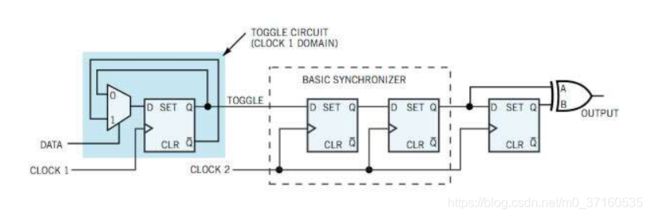
The input signal of a pulse synchronizer is a single clockwide pulse that triggers a toggle circuit in the originating clock domain (Figure 3 ). The output of the toggle circuit switches from high to low and vice versa each time it receives a pulse and passes through the level synchronizer to arrive at one input of the XOR gate, while a one-clock-cycle-delayed version goes to the other input of the XOR. For one clock cycle, each time the toggle circuit changes state, the output of this synchronizer generates a single clockwide pulse.
Figure 3 The input signal of a pulse synchronizer is a single-clock, cyclewide pulse that triggers a toggle circuit in the originating clock domain.
The basic function of a pulse synchronizer is to take a single clockwide pulse from one clock domain and create a single clockwide pulse in the new domain. One restriction of a pulse synchronizer is that input pulses must have a minimum spacing between pulses equal to two synchronizer clock periods. If the input pulses are closer, the output pulses in the new clock domain are adjacent to each other, resulting in an output pulse that is wider than one clock cycle. This problem is more severe when the clock period of input pulse is greater than twice the synchronizer clock period. In this case, if the input pulses are too close, the synchronizer does not detect every one.
Handshaking and FIFOs
In many applications, simple signals are not the only information crossing clock domains; data, address, and control buses also travel together across domains. Engineers have at their disposal additional tools, such as hand-shaking protocols and FIFOs, that can handle these situations.
Handshaking allows digital circuits to effectively communicate with each other when the response time of one or both circuits is unpredictable. For example, an arbitrated bus allows more than one circuit to request access to a single bus, such as PCI or AMBA (Advanced Microcontroller Bus Architecture), using arbitration to determine which circuit gains access to the bus. Each circuit signals a request, and the arbitration logic determines which request “wins.” This winning circuit receives an acknowledgment indicating that it has access to the bus. It then discontinues its request and begins the bus transaction.
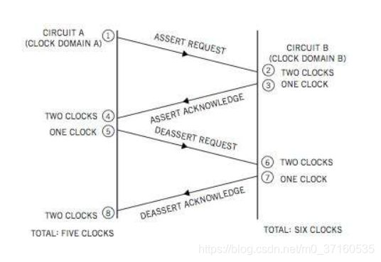
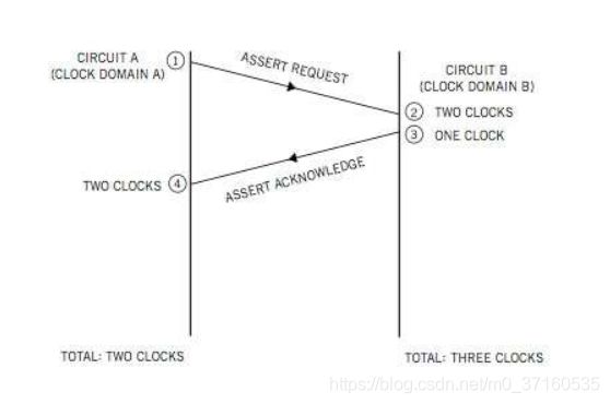
Full- and partial-handshake signaling are the two fundamental types of handshake protocol that circuits on different clock domains use. Each type of handshake uses synchronizers, and each has its own set of design trade-offs. In full-handshake signaling, the two circuits wait for each other before asserting or dropping their respective handshake signal (Figure 4 ). First, Circuit A asserts its request signal. Next, Circuit B detects that the request signal is valid and asserts its acknowledgment signal. When Circuit A detects that the acknowledgment signal is valid, it drops its request signal. Finally, when Circuit B detects that the request is invalid, it drops its acknowledgment signal. Circuit A does not make a new request until it detects that the acknowledgment signal is invalid.
Figure 4 In full-handshake signaling, the two circuits wait for each other before asserting or dropping their respective handshake signals.
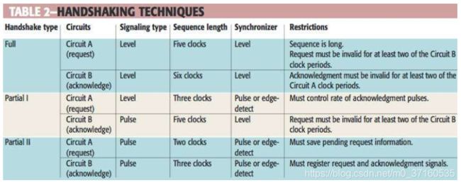
This type of handshake uses level synchronizers. A designer uses this technique when the acknowledging circuit (Circuit B) needs to inform the requesting circuit (Circuit A) that it is actively processing the request. This handshake requires that the requesting circuit hold off its next request until it detects that the acknowledgment signal is invalid. To determine the timing for this protocol, use the rules of thumb that signals take two clock cycles to cross a clock domain and that circuits register signals before they cross clock domains. The complete sequence takes a maximum of five cycles in the A clock domain plus a maximum of six cycles in the B clock domain. Full handshaking is robust because each circuit explicitly knows the state of the other by examining the request and acknowledgment signals. The drawback of this scheme is that the entire process uses many clock cycles to complete the transaction.
Partial handshaking is another signaling technique that shortens this sequence of events. With partial handshake signaling, the two circuits communicating with each other do not wait for the other one before dropping their respective signal and continuing with the handshake sequence. Partial handshaking is less robust than full handshaking because the handshake signals do not indicate the state of both circuits; each circuit must save state information normally present in full handshake signals. However, by not waiting until the other circuit drops it handshake signal, the whole sequence of events takes less time.
When using partial-handshake signaling, the acknowledging circuit must generate its signal at the correct time. If the acknowledging circuit needs to complete processing the request before it can handle another, then the timing of the acknowledgment signal is important. The circuit uses its acknowledgment signal to indicate when it completed any processing. One partial-handshake scheme mixes level and pulse signaling, and the other uses only pulse signaling.
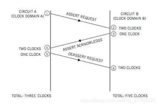
In the first partial-handshake scheme, Circuit A asserts its request signal as an active level, and Circuit B acknowledges it with a single clockwide pulse. In this case, Circuit B does not care when Circuit A drops its request signal. However, to make this technique work, Circuit A must drop its request signal for at least one clock cycle; otherwise, Circuit B cannot distinguish between a previous request and a new request. With this handshake, Circuit B uses a level synchronizer for the request signal, and Circuit A uses a pulse synchronizer for the acknowledgment signal. The acknowledgment pulses occur only when Circuit B detects the request signal. This situation allows Circuit A to control the spacing of pulses it receives into the synchronizer by controlling the timing of its request signal (Figure 5 ). Once again, to determine timing, use the rules of thumb that signals take two clock cycles to cross a clock domain and that circuits register signals before they cross clock domains.
Figure 5 In a partial-handshake scheme, Circuit A asserts its request signal, and Circuit B acknowledges it with a single clockwide pulse.
The complete sequence takes a maximum of three cycles in the A clock domain plus a maximum of five cycles in the B clock domain. This partial handshake signaling uses two fewer clock cycles in the A clock domain and one fewer clock cycle in the B clock domain than full handshake signaling. You can shave off a few more clock cycles using a second partial-handshake scheme where Circuit A asserts its request with a single clockwide pulse and Circuit B acknowledges the request with a single clockwide pulse. In this case, both circuits need to save state to indicate that the request is pending.
Figure 6 This type of partial-handshake scheme uses pulse synchronizers, but a circuit that has a clock that is twice as fast as the other can instead use an edge-detecting synchronizer.
This type of handshake uses pulse synchronizers, but either circuit that has a clock that is twice as fast as the other can instead use an edge-detecting synchronizer instead (Figure 6 ). The complete sequence takes a maximum of two cycles in the A clock domain plus a maximum of three cycles in the B clock domain. This partial-handshaking technique uses three fewer clock cycles in the A clock domain and three fewer clock cycle in the B clock domain than full-handshake signaling. This technique is also faster than the first partial-handshake signaling by one cycle in the A clock domain and two cycles in the B clock domain (Table 2 ). These handshake protocols involve single signals that cross clock domains. However, when groups of signals cross clock domains, designers need to use more complex signaling schemes.
Datapath design
One important rule when synchronizing signals is that a designshould not synchronize the same signal in more than one place; that is,a single signal fans out to more than one synchronizer. Becausesynchronization takes one to two clock cycles, a designer cannotreliably predict when each of these signals arrives across a clockdomain. In addition, the timing of a group of synchronized signals inthe new clock domain can vary because the delay can be either a singleclock cycle of delay or two cycles, depending on when the input arrivesat the synchronizer. This situation results in a “race condition”between the individually synchronized signals. This race condition alsoapplies to groups of signals, such as data, address, and control buses,that need to travel together across clock domains. Thus, you should notuse individual synchronizers on each signal in the group or on each bitof a data bus or an address bus in which each signal needs to be validin the new clock domains at the same time.
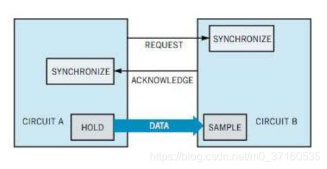
One way to solve the problem of bussynchronization is to use a holding register and handshake signaling.This circuit comprises a register that holds the signal bus and ahandshaking scheme (Figure 7 ). Thehandshake signals indicate when the circuit in the new clock domain cansample the bus and when the originating circuit can replace the currentcontents of the holding register.
Figure 7 A datapath-synchronizer design uses a holding register and hand- shake signaling.
In this design, the transmitting circuit stores the data(signal bus) in the holding register as it asserts the request signal.These two actions can happen at once because the request signal takes atleast one clock cycle before the receiving circuit detects it (theminimum handshake-synchronization delay). When the receiving circuitsamples the data (signal bus), it asserts the acknowledgment signal.This design uses full handshaking and takes a long time to complete thetransfer. A design using full-handshake signaling has a large window oftime for the receiving circuit to sample the signal bus and is thussomewhat inefficient. The same design can use a partial handshakeinstead of a full handshake to speed the transfer.
With this type of bus synchronization, you synchronize thehandshake signals but not the signal bus. The signal bus originates fromthe holding register and remains stable until after the receivingcircuit samples it. Note that bus synchronization may not work inapplications in which the transmitting circuit presents data too fastfor the receiving circuit to handle it.
Advanced datapath design
In many cases, data needs to “pile up” as it crosses clockdomains, so designs using a single holding register do not work. Onesuch case is a transmitting circuit that presents data in bursts, tooquickly for a receiving circuit to sample. Another such case is areceiving circuit that samples data faster, but in a narrower datawidth, than the transmitting circuit sends it. These situations call forthe use of a FIFO.
Fundamentally, a designer uses a FIFO for speed matching,data-width matching, or both. For speed matching, the faster port on theFIFO handles burst transfers while the slower port handles constantrate transfers. However, even with different access types and speeds,the average data rates into and out of the FIFO have to be the same;otherwise, the FIFO overflows or underflows. Like the single-registerdesign, the FIFO holds data in registers or memory while it synchronizesstatus signals that determine when data can be written into the FIFO orwhen data can be read out of it.
In speed-matching applications, each port (read or write) has adifferent clock. The registers in the FIFO use the write-port clock,just as the holding register uses the clock of the circuit changing theregister's contents. Signal synchronization takes place in the pointerlogic and is more complex than handshake signaling.
Several approaches exist for designing the pointer logic. Thefirst method is to synchronize the read and write strobes while usingcounters in each clock domain to track the available entries in theFIFO. The counters reflect the number of FIFO entries available forreading or writing, and the counters are synchronous with theirrespective ports. The read counter tracks the number of entries thatcontain valid data, and the write counter tracks the number of entriesavailable to store data. When you reset the pointer logic, the readcounter starts at zero because no data is available to read. The writecounter starts at the number of entries in the FIFO, meaning that allthe entries are available for storing data.
The read strobe decrements the read counter and issynchronized to the write-clock domain before it increments the writecounter. The write strobe decrements the write counter and issynchronized to the read-clock domain before it increments the readcounter.
This design requires single clockwide pulses and pulsesynchronizers for the read and write strobes because, as a level signalcrosses from one clock domain to a faster one, it remains valid for moreclock cycles in the faster domain than in the slow one. Because eachcounter changes whenever the read or write signal is valid, then thefaster clock domain detects more reads or writes than actually occurredin the slower clock domain. Pulse synchronizers translate a clockwidepulse in one clock domain to a clockwide pulse in the new clock domain,and each pulse represents one read or write of the FIFO.
This FIFO-status technique gives pessimistic status for bothreads and writes. The status for the write port indicates full when theFIFO has all entries filled and continues to indicate full after theread strobe triggers, because synchronization delays the strobe to thewrite counter. This situation is also true for the empty status on theread port, because synchronization delays the write strobe to the readcounter.
Another consideration for this design is detecting full orempty at the right time. If the FIFO has one entry remaining, and thewrite strobe triggers, the FIFO must then set the full status. Thisscenario gives the full indication one clock sooner to allow the circuitwriting into the FIFO enough time to stop the next write fromoverflowing the FIFO. This situation is also true for the read port ofthe FIFO. In this case, if the FIFO has only one entry, and the readstrobe triggers, you must set the empty status to give the readcircuitry time to prevent a read of an empty FIFO.
This pointer logic restricts circuits from accessing the FIFOon every clock cycle, even in the slow clock domain. The advantage ofthis feature is that the circuits accessing the FIFO have at least oneclock cycle to evaluate the FIFO status. The FIFO can have every entryfilled with data without overwriting valid data or can be empty withoutreading invalid data. Another advantage of this design is that each sidecan read its respective counter and determine how many entries areavailable. A designer can use this FIFO design for circuits that performmultiple reads or writes of data without causing an underflow oroverflow condition.
The drawback of this design is that counters, rather thandirect comparisons of the read and write pointers, determine status. Forlarge FIFOs, these counters are large. Also, the average data rates arehalf the slowest clock frequency, because the read or write pulses fromthe faster clock domain must have at least two clock periods betweenthem in the slow-clock domain when using pulse synchronizers. One way toeliminate some of these problems is to use direct pointer comparison.
In this FIFO design, comparing the read and write pointersdetermines the FIFO status. Pointer comparison in asynchronous designsis more challenging, because each pointer exists in a different clockdomain, and synchronizing a signal bus requires that the bus does notchange while synchronizing handshake signals. A FIFO design using thistechnique for pointer synchronization would be slow. To solve thisproblem, the FIFO pointer logic uses Gray code instead of binary codefor the pointers.
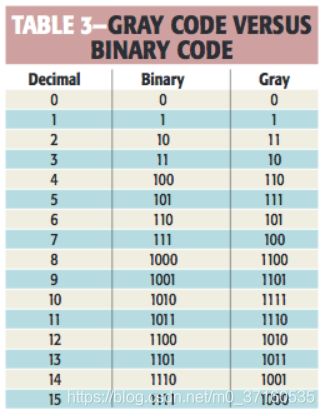
Gray code changes only one bit at a time for each increase or decrease in the count (Table 3 ).You can use synchronizers on Gray-code buses because only one signalchanges each time the bus changes, eliminating the race conditionbetween bits of the Gray-coded bus as it passes through separatesynchronizers. The pointers for this design are Gray-code counters.Using binary pointers would require synchronizing pointer values afterconverting them to Gray code, and using conversion logic violates therestriction that synchronized signals originate from flip-flops beforecrossing a clock domain.
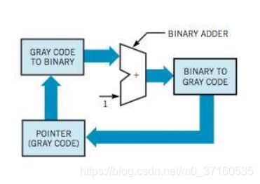
The Gray-code counter is a binary adder with converters from and to Gray code before and after the adder (Figure 8 ).Converting to and from Gray code is an XOR operation, so you need only afew more levels of logic than a binary counter. To convert Gray code tobinary, use: BN =GN ; BN –1=BN +GN –1; BN –2=BN –1+GN –2…B1 =B2 +G1 ; B0 =B1 +G0 . To convert binary to Gray code, use: GN =BN ; GN –1=BN +BN –1; GN –2=BN –1+BN –2…G1 =B2 +B1 ; G0 =B1 +B0 .A design can use the same technique to compare Gray-code pointer valuesby adding converters between the pointers and binary-comparison logic.
Figure 8 The Gray-code counter, a binary adder, has converters from and to Gray code before and after the adder.
A FIFO with this pointer logic is fast, and circuits can reador write the FIFO on every clock cycle. However, accessing the FIFO onevery cycle means the FIFO status has to include almost-full andalmost-empty indications, so that the circuits accessing the FIFO havetime to stop. Almost full indicates that one entry is available towrite, and almost empty indicates that one entry remains unread. Thissituation describes a design that needs the fewest possible statussignals, and a design needs more indicators if the circuits accessingthe FIFO use a burst access with a fixed minimum size.
This FIFO-status technique gives pessimistic status for bothreads and writes. The status on the write port indicates full when theFIFO fills and continues to indicate full after it the circuit reads it,because synchronization delays the read pointer to the write-sidecomparison logic. This situation is also true for the empty status onthe read side, because synchronization delays the write pointer to theread-side comparison logic.
Handling signals crossing clock domains becomes lesschallenging when you design with techniques that reduce the risk ofcommunication failure between circuits in different domains. To preventmetastability of flip-flops receiving signals that cross clock domainsfrom causing unpredictable behavior in circuits, use synchronization.Level synchronizers work well for signals that remain valid for manyclock cycles. Use an edge-detecting synchronizer for level signals inthe slower clock domain that change to pulses in the new clock domain.Finally, use pulse synchronizers for pulses crossing clock domains.Remember that, when a signal bus crosses clock domains, it needs toarrive in the new clock domain during the same clock cycle. Do notsynchronize each signal but use a holding register and handshaking.Handshaking indicates when signals in the holding register are valid andwhen to sample them. Using handshaking and a holding register is usefulfor data buses but does not provide for passing more than one data wordat a time to the new clock domain.
| References |
|
