肖特基二极管作用
简介:
A Schottky barrier diode differs from a conventional diode in that a metal-to-semiconductor contact between plays an important role.
肖特基二极管并不是普通的由PN节构成的二极管,而是由金属和中度参杂了N半导体材料接触而成的(摘自《微电子电路》)。
特点:
The notable properties of Schottky barrier diodes are low forward voltage drop and fast switching action. Specifically, the forward voltage drop is approximately half (about 0.3 V) and the switching duration one-tenth or less (1 ns or less) that of conventional pn junction diodes.
Therefore, Schottky barrier diodes are effective in applications such as fast switching, clamping, and clipping. In addition, their good frequency response makes them suitable for high-frequency applications.
SBD拥有低开关电压(0.3V),高速的开断转换(1ns或更低),以及良好的频率响应。
SBD的伏安特性和普通的PN节二极管类似。
SBD转换速率很快的原理:SBD中,电流由多数载流子(电子)传道,因此,并没有传统PN节中的少数载流子的电荷效应,所以SBD从导通转为截止(或反之)的速率比普通二极管快很多。
硅制成的二极管导通电压一般为0.6~0.8V,而SBD导通电压为0.3~0.5V。
作用:
Typical uses of Schottky barrier diodes include power supply circuit protection, high-frequency wave detection, and as
diode terminals. The range of applications for Schottky barrier diodes has expanded in recent years as demand for
electronic equipment with higher operating frequencies and more compact dimensions has grown. In addition, demand
is increasing for composite devices in order to increase the mounting efficiency of small devices and achieve greater
mounting density.
Schottky barrier diode applications include (1) reverse current prevention, (2) mixers, and (3) wave detectors. Each of
these applications is described below.
Reverse Current Prevention
Sometimes a diode is used to prevent damage to the system from unwanted current flow in cases where a reverse voltage is applied to the system accidentally. With the trend toward lower operating voltages, Schottky barrier diodes are often used for this purpose due to their low voltage drop. Recommended products: HSB226YP, HSC226, HSL226
Sometimes a diode is used to prevent damage to the system from unwanted current flow in cases where a reverse voltage is applied to the system accidentally. With the trend toward lower operating voltages, Schottky barrier diodes are often used for this purpose due to their low voltage drop. Recommended products: HSB226YP, HSC226, HSL226 典型应用电路可参考《ARM Linux入门与实践》P63的原理图。
Mixers
A circuit that combines two frequencies to obtain the desired frequency is called a mixer circuit.
Frequency 1 (f1) and frequency 2 (f2) are mixed to produce the desired frequency (f3). For reception a down converter, which lowers the frequency, is used. This is expressed by the equation f1 – f2 = f3. For transmission an up converter, which raises the frequency, is used. This is expressed by the equation f1 + f2 = f3. FET and IC mixer circuits are available, but circuits composed of diodes are still used as well.
An example diode mixer circuit is shown below.
• Single Balanced Mixer Circuit Using Two Diodes Recommended products: HSB88AS, HSB276AS, HSM88AS, HSM276AS, etc.
Double Balanced Mixer Circuit Using Four Diodes ,Recommended products: HSB88AS, HSB88ASR, HSM88AS, HSM88ASR, etc.
Wave Detectors
Diodes are used to detect signal levels (high-frequency power).
The principal applications include output wave detection in transmitters (power amplifiers) and wave detection in sensors.
The operating principle of diode wave detection involves rectifying the AC components constituting the signal to
generate voltage in the form of DC components.
The methods used for wave detection are zero bias detection and bias detection. Zero bias detection utilizes the nonlinear properties of the Schottky diode, while bias detection utilizes their linear properties and requires a bias circuit.
A circuit example and the detection voltage characteristics of the main products are shown below.
Diode Wave Detector Circuit (2.4 GHz)
An example zero bias detector circuit is shown below.
This type of circuit is generally called an AM detector circuit. It makes use of the non-linear properties of the Schottky diode. Such circuits are used in products such as cordless telephones, ETC systems, wireless LAN equipment, and electronic ID tags.
Recommended products: HSC285, HSD88, HSD276A, HSD278
System Protection (Surge and Noise Protection)
By connecting Schottky barrier diodes to the input pin (Vin) of an IC or LSI device, it is possible to clamp the voltage input to pin to within the allowable range, thereby preventing overvoltage surges. This can be useful for preventing system malfunctions.
SPICE Parameters
The equivalent circuit and SPICE parameters below are provided as reference when using a circuit simulator as a circuit design tool. In order to use a circuit simulator, construct the following equivalent circuit.
具体请参考文件:http://documentation.renesas.com/doc/products/diode/rej27g0023_schottkyci.pdf
以下参考:http://www.cnblogs.com/pied/archive/2010/08/02/1790288.html
参数:
MAX current peak reverse voltage 反向电压峰值
MAX RMS voltage 反向电压平均值
超过reverse voltage就会击穿。peak是峰值,rms是有效值。
MAX DC reverse current 最大反向直流电流
在未击穿状态下的电流。
MAX average forward current 最大正向平均电流
MAX forward surge current 正向最大浪涌电流
超过就可能损坏。
MAX forward voltage 最大正向压降
应用注意:
考虑到其反向电压一般<100V,所以,只适合应用于低压场合。
典型应用:
1】在BJT的开关电路里面
通过在BJT上连接Shockley二极管来箝位,使得晶体管在导通状态时其实处于很接近截至状态.从而提高晶体管的开关速度.这种方法是74LS,74ALS, 74AS等典型数字IC TTL内部电路中使用的技术.
参考如下链接:http://www.elecfans.com/dianzichangshi/2009040745174.html
抗饱和TTL电路是目前传输速度较高的一类TTL电路。这种电路由于采用肖特基势垒二极管SBD钳位方法来达到抗饱和的效果 ,一般称为SBDTTL电路(简称STTL电路),其传输速度远比基本TTL电路为高。
肖特基势垒二极管的工作特点如下:
(1)它和PN结一样,同样具有单向导电性,这种铝-硅势垒二极管导通电流的方向是从铝到硅。
(2)AL-SiSBD的导通阈值电压较低,约为0.4~0.5V ,比普通硅PN结约低0.2V。
(3)势垒二极管的导电机构是多数载流子 ,因而电荷存储效应很小。
根据前面的学习,我们已经知道,BJT工作在饱和时 ,发射结和集电结都处在正向偏置,集电结正向偏置电压越大,则表明饱和程度越深。
为了限制BJT的饱和深度,在BJT的基极和集电极并联上一个导通阈值电压较低的肖特基二极管,如下图所示。
当没有SBD时,随着基级电压的升高,电流沿着蓝线方向流动。由于SBD的作用,当基级电压大于0.4V时, SBD首先电导通,电流沿着红线方向流动(如下图所示),从而使T的基极电流不会过大(而且使T的集电结正向偏压将被钳制在0.4V左右),因此SBD起到抵抗过饱和的作用,因而又将这种电路称为抗饱和电路,使电路的开关时间大为缩短。
下图为肖特基TTL(STTL)与非门的典型电路。与基本TTL与非门电路相比,作了若干改进。在基本的TTL电路中 ,T1、T2和T3工作在深度饱和区,管内电荷存储效应对电路的开关速度影响很大。现在除T4外,其余的BJT均采用SBD钳位,以达到明显的抗饱和效果。其次,基本电路中的所有电阻值这里几乎都减半。这两项改进导致门电路的开关时间大为缩短。由于电阻值的减小也必然会引起门电路功耗的增加。
2】微波电能传输电路中的整流器件。
如蓝牙电力传输系统中的整流器件。
3】和储能元件一起使用,防止电压电流突变,提供通路。
电感可以经过它给负载提供持续的电流,以免负载电流突变,起到平滑电流的作用!在开关电源中,就能见到一个由二极管和电阻串连起来构成的的续流电路。做续流二极管时,二极管反向接入,及阴极接接供电正极。要求管子开关速度快。
这叫续流二极管,就是这样反接的!
首先,你要明白这种buck型DC/DC电路的拓扑结构:
LM2756相当于高速断开和闭合的开关,连接在Vin与Vout脚之间。
1. 在开关闭合时,电流经1脚Vin、2脚Vout、电感L1,到达+5V输出端,流到负载再到地,二极管D1反接不起作用。根据电磁感应定律,电感对突变电流起阻碍作用,电流是逐渐升高的。没等电流稳定,开关就断开了(要是等电流稳定了,输出端就不是+5V了,而是+12V直接就过来了)。
2. 当开关断开时,Vin不再提供电流到Vout。但根据电磁感应定律,电感对突变电流起阻碍作用,电感L1会产生感应电流且与原来方向相同,L1相当于电源。任何电路的电流都是要有回路的,此电感产生的感应电流总要回到电感,就是靠这个二极管回流的,其电流 经过L1、5V输出端、负载到地,再经二极管D1回到电感L1,此时二极管相对于感应电流就是正向连接了!没等这个电流消失,开关又闭合(要是电流消失,+5V就变成0V了)。

3. 重复以上过程……
4】A/D转换中的开关。
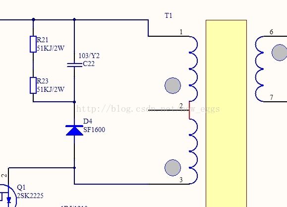
5】开关电源变压器截止时间段的电流放电(与3类似)
如下图所示: