SD/MMC 接口及上电时序
SD需要高速读写,同时也要使手持等嵌入式设备能方便使用,特设有两个访问接口中:SD模式接口和SPI接口。SD卡在上电初期,卡主控通过检测引脚1(DAT3)来决定使用SD模式还是SPI模式。当此脚接50KOhm上拉电阻时,卡进入SD模式;当此脚为低电平,卡则工作于SPI模式。
SPI Bus Mode Pad Definition
Pin Name Type1 SPI Description
1 CS I Chip Select (Active low)
2 DataIn I Host to Card Commands and Data
3 VSS S Supply Voltage Ground(can be canceled if there are only 8 pins)
4 VDD S Supply Voltage
5 CLK I Clock
6 VSS2 S Supply Voltage Ground
7 DataOut O Card to Host Data and Status
8 RSV I Reserved
9 RSV I Reserved
NOTES:
1) The ‘ RSV ’ pins are floating inputs. It is the responsibility of the host designer to connect external
pull up resistors to those lines. Otherwise non-expected high current consumption may occur due to
the floating inputs.
2)Hot insertion and removal are allowed. The SanDisk SD Card will not be damaged by inserting or removing
it into the SD bus even when the power is up:
>>The inserted card will be properly reset also when CLK carries a clock frequency fPP.
>>Data transfer failures induced by removal/insertion should be detected by the bus master using
the CRC codes that suffix every bus transaction.
3)Power Protection
>>Cards can be inserted into or removed from the bus without damage. If one of the supply pins
(VDD or VSS) is not connected properly, then the current is drawn through a data line to supply the card.
>>Data transfer operations are protected by CRC codes; therefore, any bit changes induced by card
insertion and removal can be detected by the SD bus master. The inserted card must be properly
reset also when CLK carries a clock frequency fpp. If the hot insertion feature is implemented in the host,
than the host has to withstand a shortcut between VDD and VSS without damage.
部分翻译:
2)热拔插是被允许的。当电源就绪时,SD 卡甚至不会由于在 SD 总线上拔插而损坏:
>>当 CLK 上运载一个时钟频率 fPP 时,这个插入的卡将会被正确地复位(重置)。
>>数据传送失败可能是由拔插动作导致的,应该由总线管理器在每次总线传送的尾部加上 CRC 编码来侦测
(用于确认每次的传送是否成功)。
3)电源保护
>>卡可以在总线上拔插而不会损坏。如果一条电源供应引脚(VDD 或 VSS)没能正确连接上,则电流将通过数据线
汲取而供应到卡上。
>>数据传送操作是通过 CRC 编码来保护的,因此,由拔插卡引起的任何位的变动将会被 SD 总线管理器侦测到。
当 CLK 上运载一个时钟频率 fPP 时,这个插入的卡必须要正确地复位(重置)。如果这个热插入特性是在主机
内实现的,则该主机要经得起 VDD 和 VSS 之间短路而不损坏。
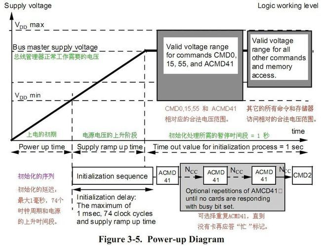
上电时序如图:(SPI模式不支持CMD15,详见SD/MMC card 命令)
