12、CubeMx STM32H750VB FMC
重要提醒:FMC时MPU需设置为Device memory或者Strongly ordered memory


CubeMx配置:


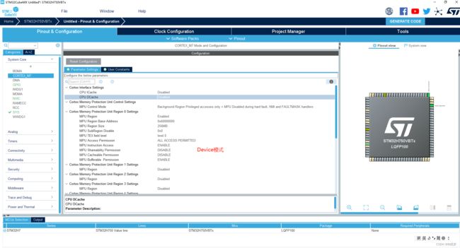


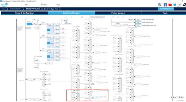
其余默认
生成工程,注意此处FMC配置关闭了Write FIFO,建议打开,对时序不影响
代码测试
添加测试代码
typedef struct
{
  volatile uint16_t LCD_REG;
  volatile uint16_t LCD_RAM;
} LCD_TypeDef;

#define LCD_BASE        ((uint32_t)(0x60000000 | 0x0007FFFE))
#define LCD ((LCD_TypeDef *) LCD_BASE)

void TestSRAM(void)
{
  volatile uint16_t x = 0;

  x = LCD->LCD_REG;
  x = LCD->LCD_RAM;
  LCD->LCD_REG = 0x00;
  LCD->LCD_RAM = 0x00;
}
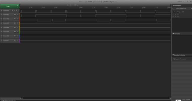
main的while(1)一直执行TestSRAM()
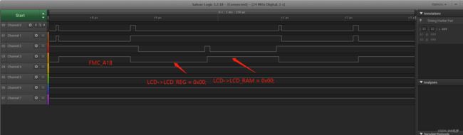
测试效果:
第一条通道是片选引脚,其余两条是读写使能
打开FMC的FIFO测试波形也是一致的,
hsram1.Init.WriteFifo = FMC_WRITE_FIFO_ENABLE;
建议打开


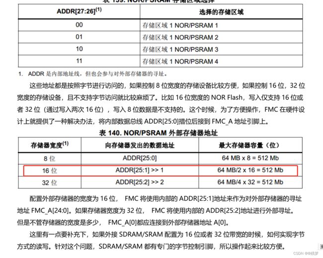
关于FMC_A18的电平信号解释

代码工程
main.c
/* USER CODE BEGIN Header */
/**
  ******************************************************************************
  * @file           : main.c
  * @brief          : Main program body
  ******************************************************************************
  * @attention
  *
  * © Copyright (c) 2023 STMicroelectronics.
  * All rights reserved.
  *
  * This software component is licensed by ST under BSD 3-Clause license,
  * the "License"; You may not use this file except in compliance with the
  * License. You may obtain a copy of the License at:
  *                        opensource.org/licenses/BSD-3-Clause
  *
  ******************************************************************************
  */
/* USER CODE END Header */
/* Includes ------------------------------------------------------------------*/
#include "main.h"
#include "gpio.h"
#include "fmc.h"

/* Private includes ----------------------------------------------------------*/
/* USER CODE BEGIN Includes */

/* USER CODE END Includes */

/* Private typedef -----------------------------------------------------------*/
/* USER CODE BEGIN PTD */

/* USER CODE END PTD */

/* Private define ------------------------------------------------------------*/
/* USER CODE BEGIN PD */
/* USER CODE END PD */

/* Private macro -------------------------------------------------------------*/
/* USER CODE BEGIN PM */

/* USER CODE END PM */

/* Private variables ---------------------------------------------------------*/

/* USER CODE BEGIN PV */

/* USER CODE END PV */

/* Private function prototypes -----------------------------------------------*/
void SystemClock_Config(void);
static void MPU_Config(void);
/* USER CODE BEGIN PFP */

/* USER CODE END PFP */

/* Private user code ---------------------------------------------------------*/
/* USER CODE BEGIN 0 */
typedef struct
{
  volatile uint16_t LCD_REG;
  volatile uint16_t LCD_RAM;
} LCD_TypeDef;

#define LCD_BASE        ((uint32_t)(0x60000000 | 0x0007FFFE))
#define LCD ((LCD_TypeDef *) LCD_BASE)

void TestSRAM(void)
{
  volatile uint16_t x = 0;

  x = LCD->LCD_REG;
  x = LCD->LCD_RAM;
  LCD->LCD_REG = 0x00;
  LCD->LCD_RAM = 0x00;
}
/* USER CODE END 0 */

/**
  * @brief  The application entry point.
  * @retval int
  */
int main(void)
{
  /* USER CODE BEGIN 1 */

  /* USER CODE END 1 */

  /* MPU Configuration--------------------------------------------------------*/
  MPU_Config();

  /* MCU Configuration--------------------------------------------------------*/

  /* Reset of all peripherals, Initializes the Flash interface and the Systick. */
  HAL_Init();

  /* USER CODE BEGIN Init */

  /* USER CODE END Init */

  /* Configure the system clock */
  SystemClock_Config();

  /* USER CODE BEGIN SysInit */

  /* USER CODE END SysInit */

  /* Initialize all configured peripherals */
  MX_GPIO_Init();
  MX_FMC_Init();
  /* USER CODE BEGIN 2 */

  /* USER CODE END 2 */

  /* Infinite loop */
  /* USER CODE BEGIN WHILE */
  while (1)
  {
    /* USER CODE END WHILE */

    /* USER CODE BEGIN 3 */
    TestSRAM();
  }
  /* USER CODE END 3 */
}

/**
  * @brief System Clock Configuration
  * @retval None
  */
void SystemClock_Config(void)
{
  RCC_OscInitTypeDef RCC_OscInitStruct = {0};
  RCC_ClkInitTypeDef RCC_ClkInitStruct = {0};

  /** Supply configuration update enable
  */
  HAL_PWREx_ConfigSupply(PWR_LDO_SUPPLY);
  /** Configure the main internal regulator output voltage
  */
  __HAL_PWR_VOLTAGESCALING_CONFIG(PWR_REGULATOR_VOLTAGE_SCALE0);

  while(!__HAL_PWR_GET_FLAG(PWR_FLAG_VOSRDY)) {}
  /** Initializes the RCC Oscillators according to the specified parameters
  * in the RCC_OscInitTypeDef structure.
  */
  RCC_OscInitStruct.OscillatorType = RCC_OSCILLATORTYPE_HSI;
  RCC_OscInitStruct.HSIState = RCC_HSI_DIV1;
  RCC_OscInitStruct.HSICalibrationValue = RCC_HSICALIBRATION_DEFAULT;
  RCC_OscInitStruct.PLL.PLLState = RCC_PLL_ON;
  RCC_OscInitStruct.PLL.PLLSource = RCC_PLLSOURCE_HSI;
  RCC_OscInitStruct.PLL.PLLM = 4;
  RCC_OscInitStruct.PLL.PLLN = 60;
  RCC_OscInitStruct.PLL.PLLP = 2;
  RCC_OscInitStruct.PLL.PLLQ = 2;
  RCC_OscInitStruct.PLL.PLLR = 2;
  RCC_OscInitStruct.PLL.PLLRGE = RCC_PLL1VCIRANGE_3;
  RCC_OscInitStruct.PLL.PLLVCOSEL = RCC_PLL1VCOWIDE;
  RCC_OscInitStruct.PLL.PLLFRACN = 0;
  if (HAL_RCC_OscConfig(&RCC_OscInitStruct) != HAL_OK)
  {
    Error_Handler();
  }
  /** Initializes the CPU, AHB and APB buses clocks
  */
  RCC_ClkInitStruct.ClockType = RCC_CLOCKTYPE_HCLK|RCC_CLOCKTYPE_SYSCLK
                              |RCC_CLOCKTYPE_PCLK1|RCC_CLOCKTYPE_PCLK2
                              |RCC_CLOCKTYPE_D3PCLK1|RCC_CLOCKTYPE_D1PCLK1;
  RCC_ClkInitStruct.SYSCLKSource = RCC_SYSCLKSOURCE_PLLCLK;
  RCC_ClkInitStruct.SYSCLKDivider = RCC_SYSCLK_DIV1;
  RCC_ClkInitStruct.AHBCLKDivider = RCC_HCLK_DIV2;
  RCC_ClkInitStruct.APB3CLKDivider = RCC_APB3_DIV2;
  RCC_ClkInitStruct.APB1CLKDivider = RCC_APB1_DIV2;
  RCC_ClkInitStruct.APB2CLKDivider = RCC_APB2_DIV2;
  RCC_ClkInitStruct.APB4CLKDivider = RCC_APB4_DIV2;

  if (HAL_RCC_ClockConfig(&RCC_ClkInitStruct, FLASH_LATENCY_4) != HAL_OK)
  {
    Error_Handler();
  }
}

/* USER CODE BEGIN 4 */

/* USER CODE END 4 */

/* MPU Configuration */

void MPU_Config(void)
{
  MPU_Region_InitTypeDef MPU_InitStruct = {0};

  /* Disables the MPU */
  HAL_MPU_Disable();
  /** Initializes and configures the Region and the memory to be protected
  */
  MPU_InitStruct.Enable = MPU_REGION_ENABLE;
  MPU_InitStruct.Number = MPU_REGION_NUMBER0;
  MPU_InitStruct.BaseAddress = 0x60000000;
  MPU_InitStruct.Size = MPU_REGION_SIZE_256MB;
  MPU_InitStruct.SubRegionDisable = 0x0;
  MPU_InitStruct.TypeExtField = MPU_TEX_LEVEL0;
  MPU_InitStruct.AccessPermission = MPU_REGION_FULL_ACCESS;
  MPU_InitStruct.DisableExec = MPU_INSTRUCTION_ACCESS_ENABLE;
  MPU_InitStruct.IsShareable = MPU_ACCESS_NOT_SHAREABLE;
  MPU_InitStruct.IsCacheable = MPU_ACCESS_NOT_CACHEABLE;
  MPU_InitStruct.IsBufferable = MPU_ACCESS_BUFFERABLE;

  HAL_MPU_ConfigRegion(&MPU_InitStruct);
  /* Enables the MPU */
  HAL_MPU_Enable(MPU_PRIVILEGED_DEFAULT);

}

/**
  * @brief  This function is executed in case of error occurrence.
  * @retval None
  */
void Error_Handler(void)
{
  /* USER CODE BEGIN Error_Handler_Debug */
  /* User can add his own implementation to report the HAL error return state */
  __disable_irq();
  while (1)
  {
  }
  /* USER CODE END Error_Handler_Debug */
}

#ifdef  USE_FULL_ASSERT
/**
  * @brief  Reports the name of the source file and the source line number
  *         where the assert_param error has occurred.
  * @param  file: pointer to the source file name
  * @param  line: assert_param error line source number
  * @retval None
  */
void assert_failed(uint8_t *file, uint32_t line)
{
  /* USER CODE BEGIN 6 */
  /* User can add his own implementation to report the file name and line number,
     ex: printf("Wrong parameters value: file %s on line %d\r\n", file, line) */
  /* USER CODE END 6 */
}
#endif /* USE_FULL_ASSERT */

/************************ (C) COPYRIGHT STMicroelectronics *****END OF FILE****/
fmc.c
/**
  ******************************************************************************
  * File Name          : FMC.c
  * Description        : This file provides code for the configuration
  *                      of the FMC peripheral.
  ******************************************************************************
  * @attention
  *
  * © Copyright (c) 2023 STMicroelectronics.
  * All rights reserved.
  *
  * This software component is licensed by ST under BSD 3-Clause license,
  * the "License"; You may not use this file except in compliance with the
  * License. You may obtain a copy of the License at:
  *                        opensource.org/licenses/BSD-3-Clause
  *
  ******************************************************************************
  */

/* Includes ------------------------------------------------------------------*/
#include "fmc.h"

/* USER CODE BEGIN 0 */

/* USER CODE END 0 */

SRAM_HandleTypeDef hsram1;

/* FMC initialization function */
void MX_FMC_Init(void)
{
  /* USER CODE BEGIN FMC_Init 0 */

  /* USER CODE END FMC_Init 0 */

  FMC_NORSRAM_TimingTypeDef Timing = {0};

  /* USER CODE BEGIN FMC_Init 1 */

  /* USER CODE END FMC_Init 1 */

  /** Perform the SRAM1 memory initialization sequence
  */
  hsram1.Instance = FMC_NORSRAM_DEVICE;
  hsram1.Extended = FMC_NORSRAM_EXTENDED_DEVICE;
  /* hsram1.Init */
  hsram1.Init.NSBank = FMC_NORSRAM_BANK1;
  hsram1.Init.DataAddressMux = FMC_DATA_ADDRESS_MUX_DISABLE;
  hsram1.Init.MemoryType = FMC_MEMORY_TYPE_SRAM;
  hsram1.Init.MemoryDataWidth = FMC_NORSRAM_MEM_BUS_WIDTH_16;
  hsram1.Init.BurstAccessMode = FMC_BURST_ACCESS_MODE_DISABLE;
  hsram1.Init.WaitSignalPolarity = FMC_WAIT_SIGNAL_POLARITY_LOW;
  hsram1.Init.WaitSignalActive = FMC_WAIT_TIMING_BEFORE_WS;
  hsram1.Init.WriteOperation = FMC_WRITE_OPERATION_ENABLE;
  hsram1.Init.WaitSignal = FMC_WAIT_SIGNAL_DISABLE;
  hsram1.Init.ExtendedMode = FMC_EXTENDED_MODE_DISABLE;
  hsram1.Init.AsynchronousWait = FMC_ASYNCHRONOUS_WAIT_DISABLE;
  hsram1.Init.WriteBurst = FMC_WRITE_BURST_DISABLE;
  hsram1.Init.ContinuousClock = FMC_CONTINUOUS_CLOCK_SYNC_ONLY;
  hsram1.Init.WriteFifo = FMC_WRITE_FIFO_ENABLE;
  hsram1.Init.PageSize = FMC_PAGE_SIZE_NONE;
  /* Timing */
  Timing.AddressSetupTime = 15;
  Timing.AddressHoldTime = 15;
  Timing.DataSetupTime = 255;
  Timing.BusTurnAroundDuration = 15;
  Timing.CLKDivision = 16;
  Timing.DataLatency = 17;
  Timing.AccessMode = FMC_ACCESS_MODE_A;
  /* ExtTiming */

  if (HAL_SRAM_Init(&hsram1, &Timing, NULL) != HAL_OK)
  {
    Error_Handler( );
  }

  /* USER CODE BEGIN FMC_Init 2 */

  /* USER CODE END FMC_Init 2 */
}

static uint32_t FMC_Initialized = 0;

static void HAL_FMC_MspInit(void){
  /* USER CODE BEGIN FMC_MspInit 0 */

  /* USER CODE END FMC_MspInit 0 */
  GPIO_InitTypeDef GPIO_InitStruct = {0};
  if (FMC_Initialized) {
    return;
  }
  FMC_Initialized = 1;
  RCC_PeriphCLKInitTypeDef PeriphClkInitStruct = {0};

  /** Initializes the peripherals clock
  */
    PeriphClkInitStruct.PeriphClockSelection = RCC_PERIPHCLK_FMC;
    PeriphClkInitStruct.FmcClockSelection = RCC_FMCCLKSOURCE_D1HCLK;
    if (HAL_RCCEx_PeriphCLKConfig(&PeriphClkInitStruct) != HAL_OK)
    {
      Error_Handler();
    }

  /* Peripheral clock enable */
  __HAL_RCC_FMC_CLK_ENABLE();

  /** FMC GPIO Configuration
  PE7   ------> FMC_D4
  PE8   ------> FMC_D5
  PE9   ------> FMC_D6
  PE10   ------> FMC_D7
  PE11   ------> FMC_D8
  PE12   ------> FMC_D9
  PE13   ------> FMC_D10
  PE14   ------> FMC_D11
  PE15   ------> FMC_D12
  PD8   ------> FMC_D13
  PD9   ------> FMC_D14
  PD10   ------> FMC_D15
  PD13   ------> FMC_A18
  PD14   ------> FMC_D0
  PD15   ------> FMC_D1
  PC7   ------> FMC_NE1
  PD0   ------> FMC_D2
  PD1   ------> FMC_D3
  PD4   ------> FMC_NOE
  PD5   ------> FMC_NWE
  */
  /* GPIO_InitStruct */
  GPIO_InitStruct.Pin = GPIO_PIN_7|GPIO_PIN_8|GPIO_PIN_9|GPIO_PIN_10
                          |GPIO_PIN_11|GPIO_PIN_12|GPIO_PIN_13|GPIO_PIN_14
                          |GPIO_PIN_15;
  GPIO_InitStruct.Mode = GPIO_MODE_AF_PP;
  GPIO_InitStruct.Pull = GPIO_NOPULL;
  GPIO_InitStruct.Speed = GPIO_SPEED_FREQ_VERY_HIGH;
  GPIO_InitStruct.Alternate = GPIO_AF12_FMC;

  HAL_GPIO_Init(GPIOE, &GPIO_InitStruct);

  /* GPIO_InitStruct */
  GPIO_InitStruct.Pin = GPIO_PIN_8|GPIO_PIN_9|GPIO_PIN_10|GPIO_PIN_13
                          |GPIO_PIN_14|GPIO_PIN_15|GPIO_PIN_0|GPIO_PIN_1
                          |GPIO_PIN_4|GPIO_PIN_5;
  GPIO_InitStruct.Mode = GPIO_MODE_AF_PP;
  GPIO_InitStruct.Pull = GPIO_NOPULL;
  GPIO_InitStruct.Speed = GPIO_SPEED_FREQ_VERY_HIGH;
  GPIO_InitStruct.Alternate = GPIO_AF12_FMC;

  HAL_GPIO_Init(GPIOD, &GPIO_InitStruct);

  /* GPIO_InitStruct */
  GPIO_InitStruct.Pin = GPIO_PIN_7;
  GPIO_InitStruct.Mode = GPIO_MODE_AF_PP;
  GPIO_InitStruct.Pull = GPIO_NOPULL;
  GPIO_InitStruct.Speed = GPIO_SPEED_FREQ_VERY_HIGH;
  GPIO_InitStruct.Alternate = GPIO_AF9_FMC;

  HAL_GPIO_Init(GPIOC, &GPIO_InitStruct);

  /* USER CODE BEGIN FMC_MspInit 1 */

  /* USER CODE END FMC_MspInit 1 */
}

void HAL_SRAM_MspInit(SRAM_HandleTypeDef* sramHandle){
  /* USER CODE BEGIN SRAM_MspInit 0 */

  /* USER CODE END SRAM_MspInit 0 */
  HAL_FMC_MspInit();
  /* USER CODE BEGIN SRAM_MspInit 1 */

  /* USER CODE END SRAM_MspInit 1 */
}

static uint32_t FMC_DeInitialized = 0;

static void HAL_FMC_MspDeInit(void){
  /* USER CODE BEGIN FMC_MspDeInit 0 */

  /* USER CODE END FMC_MspDeInit 0 */
  if (FMC_DeInitialized) {
    return;
  }
  FMC_DeInitialized = 1;
  /* Peripheral clock enable */
  __HAL_RCC_FMC_CLK_DISABLE();

  /** FMC GPIO Configuration
  PE7   ------> FMC_D4
  PE8   ------> FMC_D5
  PE9   ------> FMC_D6
  PE10   ------> FMC_D7
  PE11   ------> FMC_D8
  PE12   ------> FMC_D9
  PE13   ------> FMC_D10
  PE14   ------> FMC_D11
  PE15   ------> FMC_D12
  PD8   ------> FMC_D13
  PD9   ------> FMC_D14
  PD10   ------> FMC_D15
  PD13   ------> FMC_A18
  PD14   ------> FMC_D0
  PD15   ------> FMC_D1
  PC7   ------> FMC_NE1
  PD0   ------> FMC_D2
  PD1   ------> FMC_D3
  PD4   ------> FMC_NOE
  PD5   ------> FMC_NWE
  */

  HAL_GPIO_DeInit(GPIOE, GPIO_PIN_7|GPIO_PIN_8|GPIO_PIN_9|GPIO_PIN_10
                          |GPIO_PIN_11|GPIO_PIN_12|GPIO_PIN_13|GPIO_PIN_14
                          |GPIO_PIN_15);

  HAL_GPIO_DeInit(GPIOD, GPIO_PIN_8|GPIO_PIN_9|GPIO_PIN_10|GPIO_PIN_13
                          |GPIO_PIN_14|GPIO_PIN_15|GPIO_PIN_0|GPIO_PIN_1
                          |GPIO_PIN_4|GPIO_PIN_5);

  HAL_GPIO_DeInit(GPIOC, GPIO_PIN_7);

  /* USER CODE BEGIN FMC_MspDeInit 1 */

  /* USER CODE END FMC_MspDeInit 1 */
}

void HAL_SRAM_MspDeInit(SRAM_HandleTypeDef* sramHandle){
  /* USER CODE BEGIN SRAM_MspDeInit 0 */

  /* USER CODE END SRAM_MspDeInit 0 */
  HAL_FMC_MspDeInit();
  /* USER CODE BEGIN SRAM_MspDeInit 1 */

  /* USER CODE END SRAM_MspDeInit 1 */
}
/**
  * @}
  */

/**
  * @}
  */

/************************ (C) COPYRIGHT STMicroelectronics *****END OF FILE****/
完整工程:
链接:https://pan.baidu.com/s/1LtSXO8EayLstovmSQWh9fg
提取码:xvi4