- Android-Layout Inspector使用手册
每次的天空
android学习
LayoutInspectorAndroidLayoutInspector是AndroidStudio中用于调试应用布局的工具启动方法:通过下载LayoutInspector插件,在“View-ToolWindows-LayoutInspector”或“Tools-LayoutInspector”启动。主要界面区域:ComponentTree:显示布局中视图的层次结构,帮助直观查看应用中的元素及其
- python 实战 grpc
Avaricious_Bear
python开发语言
title:grpc|python实战grpcdescription:只要代码可以跑起来,很多难题都会迎刃而解.so,keepcodingandstayhungry.grpc的基础:protobufgrpchelloworld:python实战grpc环境配置grpcbasic:grpc4种通信方式grpc的基础:protobufgrpc使用protobuf进行数据传输.protobuf是一种数据
- 嘉为蓝鲸可观测系列产品入选Gartner《中国智能IT监控与日志分析工具市场指南》
嘉为蓝鲸
可观测嘉为蓝鲸智能运维Gartner可观测
直达原文:嘉为蓝鲸可观测系列产品入选Gartner《中国智能IT监控与日志分析工具市场指南》2025年5月,国际研究机构Gartner发布了《中国智能IT监控与日志分析工具市场指南》(MarketGuideforIntelligentITMonitoringandLogAnalysisToolsinChina),嘉为蓝鲸全栈智能可观测中心·鲸眼凭借嘉为蓝鲸日志中心与嘉为蓝鲸应用性能观测中心(APM
- vue3 vs asp.net mvc
fyifei0558
开发语言
package.json≈.csprojpackage-lock.json≈packages.lock.jsonvite.config.js≈Startup.cs/Program.cs/configfilesindex.html≈_Layout.cshtmlpublic/≈wwwroot/
- VLAN的配置
我是渣渣辉
网络
第一步,在交换机上创建VLAN配置命令[sw1]vlan2-----创建vlan2;默认情况下交换机存在vlan1,并且所有接口属于vlan1VIDVLANID:用来标识和区分VLAN取值范围0-4095;其中,0和4095保留不能使用,可使用的范围是1-4094[sw1]vlanbatch41020----同时批量的创建vlan4、10、20[sw1]vlanbatch30to60—同时批量的创
- Qt QML实现Windows桌面歌词动态播放效果
luoyayun361
QtQMLqtQt歌词播放效果
前言使用Qt5.15.2,QML实现简单的歌词动态播放效果。效果图如下:注:这里只是为了演示播放效果,并未真正加载音频进行播放。可以在此基础上进行扩展。正文关键代码QML部分importQtQuick2.15importQtQuick.Window2.15importQtQuick.Controls2.15importQtQuick.Layouts1.15importLyricsPlayback1
- 国产信创电脑如何查看IP地址、网关、DNS等信息
yeliuxiaozi
tcp/ip服务器网络协议
我的是清华同方TF830,可以直接使用命令查看!右击桌面,打开终端,键入命令nmclidevshow文章来自:https://techzhi.com/7.htmsxszf@sxszf-CX-TF830-Series:~/桌面$nmclidevshowGENERAL.设备:enp125s0f1GENERAL.类型:ethernetGENERAL.硬盘:F4:DE:AF:AD:8B:BEGENERAL
- 信创电脑|暴雨新增兆芯KX-7000处理器版本
BAOYUCompany
电脑
IT世界5月15日消息,暴雨公司信创家族新上架了一款搭载兆芯KX-7000系列处理器、摩尔线程8GB显卡、16GDDR5内存以及512GSSD的新配置台式电脑主机。兆芯KX-7000处理器采用开先的8核Chiplet互联架构,最高频率3.7GHz,拥有32MB的L3缓存容量,功耗达65~148W。除此之外,这款机型采用16GBDDR55600双通道内存,配备350W80Plus白金电源。这款机型采
- 常规层叠设计需要了解的板材知识
电子连接器有限元仿真CAE与高频分析
信号完整性分析常规层叠设计需要了解的板材知识
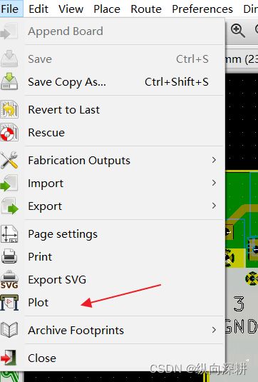
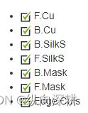
常规层叠设计需要了解的板材知识:层叠设计的第一个关键要点就是要了解板材的基本知识。观点:PCB是由铜箔(“皮”)、树脂(“筋”)、玻璃纤维布及其他功能性补强添加物(“骨”)组成。层叠设计时,要对“筋骨皮”的材料特性参数有一定了解。先来看看“皮”,在对常规层叠进行设计时,我们最关心的是铜箔的厚度,常用单位是盎司(oz),1盎司=28.350克。盎司本来是重量单位,用于叠层的时候是这么定义的:1oz的
- (提升职业竞争力)设计师的“隐藏菜单”:5个Adobe冷门技巧,重塑你的工作流
top_designer
adobe数据库前端photoshopillustratorInDesign
最近有幸深度体验了奥地利BlueskyyNationalAcademyofArts提供的Adobe正版教育订阅,感触颇深,这里和大家分享一些心得,或许能带来些新启发。关于Firefly:这应该是我接触过的最慷慨的版本,直接给了1500点创成式积分,创作自由度相当高。设备数量:最多支持4台设备激活。坦白说,我个人并没有那么多设备来测试(毕竟预算有限)。订阅透明度:这是我最欣赏的一点。学校的IT服务网
- Android 控件 - gravity 属性与 layout_gravity 属性
我命由我12345
Android-简化编程androidjavajava-ee安卓android-studio开发语言androidstudio
一、gravity属性1、基本介绍gravity属性用于控制View内部的内容的对齐方式作用对象是View内部的内容,例如,文本、子View等常用值说明left水平方向左对齐right水平方向右对齐start水平方向左对齐(RTL)end水平方向右对齐(RTL)top垂直方向顶部对齐bottom垂直方向底部对齐center_horizontal水平方向居中center_vertical垂直方向居中
- 来聊聊CST(CST Studio Suite)电路仿真(一)
思茂信息
CST电磁仿真教程性能优化网络人工智能算法windows服务器
首先我来提出一个疑问:在CST3D界面中,我在两个金属之间添加一个离散端口(discreteport),而在电路图(schematic)界面中只出现了一个端口,那么如何添加两个pin的电阻元件呢?本期我们来浅谈一下电路图中的端口究竟为何物。1、Port——天涯若比邻3D界面创建的Port是连接3D界面和电路图界面的接口。如下图所示,这里有三条PCB走线,各自串联一个port,分别为port①、po
- 谈谈国产化信创未来的发展趋势和程序员的选择
信创天地
职场和发展创业创新运维开发java-ee
国产化信创(信息技术应用创新)未来的发展趋势与程序员的选择密切相关。以下从发展趋势和程序员的选择两个方面进行分析:---一、国产化信创未来的发展趋势1.政策支持与市场驱动-政策推动:国家持续出台政策支持信创产业发展,如“十四五”规划强调自主创新和核心技术突破,信创产业成为国家战略的重要组成部分。-市场需求:随着国际形势变化,国内企业对自主可控的信息技术需求增加,信创产品在政府、金融、能源等关键领域
- 信创国产化数据库有哪些?和MySQL数据有啥区别?
信创天地
创业创新职场和发展运维开发mysql
信创国产化数据库是中国自主研发的数据库产品,旨在满足国内对数据安全和自主可控的需求。以下是一些主要的信创国产化数据库及其与MySQL的区别:主要信创国产化数据库1.达梦数据库(DM)-特点:支持多种数据类型和复杂查询,具备高安全性和高可用性。-应用场景:广泛应用于政府、金融、电信等领域。2.人大金仓(Kingbase)-特点:兼容SQL标准,支持多种操作系统和硬件平台,具备高并发处理能力。-应用场
- 信创时代技术栈选择与前景分析:国产替代背景下的战略路径与实践指南
猿享天开
信创开发系统安全科技创业创新开发语言
博主简介:CSDN博客专家、CSDN平台优质创作者,高级开发工程师,数学专业,10年以上C/C++,C#,Java等多种编程语言开发经验,拥有高级工程师证书;擅长C/C++、C#等开发语言,熟悉Java常用开发技术,能熟练应用常用数据库SQLserver,Oracle,mysql,postgresql等进行开发应用,熟悉DICOM医学影像及DICOM协议,业余时间自学JavaScript,Vue,
- 信创背景下,企业国产化在低代码平台上如何实现?
热心市民赵女士
数据库java开发语言
编者按:在国家政策及战略方向的指导下,信创产业已成为奠定中国未来发展的重要数字基础,而国产化则可以解决核心技术关键被“卡脖子”的问题。另一方面,低代码平台能够为企业加速交付业务应用,降低运营成本,已经成为加速数字化转型、适应未来发展的关键技术。低代码是一场针对软件开发的“效率革命”,而信创是剑指中国IT产业的“安全自主”,两者看似不相关,实则紧密相联。Myapps低代码平台作为有着将近20年开发经
- 第七节 移动端适配-视口与REM布局
泽泽爱旅行
csshtml前端css
以下是关于移动端适配中的视口与REM布局的全面解析,结合核心原理、实现方案、应用场景及优化策略,帮助开发者深入理解并高效实现响应式设计。一、视口(Viewport)的核心概念1.视口类型布局视口(LayoutViewport)浏览器默认的视口宽度(通常为980px),用于在移动端显示PC页面,需缩放才能适应屏幕。视觉视口(VisualViewport)用户当前可见的屏幕区域,随缩放或滚动变化。理想
- 物流涂层科技赋能仓储:创冷科技引领高温环境下的仓储物流安全升级
lingling009
科技安全网络
前言:创冷科技物流涂层解决方案破解仓储高温难题。了解热敏感货物防护、设备耐热改造及数字孪生管理等创新实践,降低23%货损率,提升21%作业效率。高温仓储危机:亟待突破的行业痛点当气温突破40℃时,钢构仓库内部温度可达60℃——巧克力融化、锂电池自燃风险激增、搬运工心率普遍超标。权威数据显示:夏季货损率平均上升23%⏳仓储效率下降17%中暑工伤赔偿激增40%物流涂层技术与智能温控系统正成为破局关键。
- 文档处理控件Aspose.Words教程:在.NET中将多页文档转换为单个图像
CodeCraft Studio
控件文档管理AsposeAspose.Wordsword文档转换Word文档处理
在Aspose.Wordsfor.NET25.6版本中,我们引入了一项新功能,允许您将多页文档导出为单个光栅图像。当您需要将文档作为单个可视文件共享或显示时,此功能非常有用。Aspose.Wordsfor.NET25.6的新功能在25.6版之前,将多页文档保存为图像格式(例如PNG或JPEG)只会为文档的第一页创建一张图片。现在,您可以使用新的MultiPageLayout类将所有文档页面合并为一
- java工程师面试题大全-100%公司笔试题你都能碰到几个
javaPie
Javaid="cproIframe_u788097_1"width="336"height="280"src="http://pos.baidu.com/acom?adn=3&at=166&aurl=&cad=1&ccd=24&cec=UTF-8&cfv=16&ch=0&col=zh-CN&conOP=0&cpa=1&dai=1&dis=0&layout_filter=rank%2Ctabclo
- 一个实验室走出15位AI创业者,华人占1/3,集齐大模型机器人搜索,教授骄傲晒战绩
强化学习曾小健
人工智能
一个实验室走出15位AI创业者,华人占1/3,集齐大模型机器人搜索,教授骄傲晒战绩原创陈骏达智东西2025年03月14日18:08北京导师不仅传道授业解惑,还是创业搭子与投资人。作者|陈骏达编辑|心缘一个AI实验室,走出15位创业者,12家知名AI创企,这是什么水平?智东西3月14日报道,昨日,加州大学伯克利分校教授PieterAbbeel在社交媒体平台上发文,盘点了从他实验室走出的15名知名AI
- 《内心强大不怯场》读书笔记1
mitt_
笔记
1.树立理想:尽早确定可奋斗的理想,有野心才能驱动行动。2.面对不如意,积极行动比抱怨更能解决问题。3.希望是生活前进动力,绝境中也别放弃希望。4.提前按理想状态生活,能更快接近梦想。5.别把命运交给他人,努力为自己当家做主。6.人生难有顺遂,无论普通人还是成功者遇挫折,要主动迎接命运,勇敢面对才能主宰命运。7.艰难坎坷的遇境能促人成长,面对命运应改变态度,提升自我,坚持跨越困难。8.改变命运需大
- 《开窍·开悟·开智》读书笔记
mitt_
笔记
1.打破常规思维,不被习惯束缚去看待事情。2.真是自己的情绪,别让负面情绪主导行为。3.真诚倾听他人观点,别急于表达自己。4.制定清晰计划,合理分配时间,提高效率。5.全面认识自己,挖掘潜在优势和隐藏不足。6.运用一些方法训练专注力,如限时任务。7.用积极乐观的心态,主动迎接挑战。8.与他人交往多付出真心,而非只考虑自身利益。9.树立终身学习观念,不断更新知识储备。10.面对压力通过运动,倾诉等方
- HarmonyOS NEXT仓颉开发语言实战案例:银行App
harmonyos-next
仓颉语言的商城项目基本开发结束啦,今天跟大家分享新的项目,一个银行app,说是新项目但是大家可能会有些眼熟,在ArkTS的教程中就写过这个项目。今天我们仓颉语言再写一遍,看看和ArkTS有什么不同。首先我们可以看到页面内容撑满了屏幕,所以需要设置沉浸模式,具体代码如下:windowStage.getMainWindow().setWindowLayoutFullScreen(true)接下来来到页
- linux进程管理
ઈ一笑ഒ
linux
一、概念1.程序:程序(program)是存放在磁盘文件中的可执行文件。2.进程:程序的执行实例被称为进程(process)。3.进程ID:进程都一定有一个唯一的数字标识符,称为进程PID(processID)。进程ID总是一非负整数。(id上限65535,在每一次重新运行都是随机分配)4.结构:linux中进程包含PCB(进程控制块)、程序以及程序所操纵的数据结构集,可分为“代码段”、“数据段”
- 工业革命推荐书籍
KevinOlivi
AI工业革命人工智能
金融领域的第四次工业革命就是“区块链”,经济领域的第四次工业革命就是“双创”(大众创新、万众创业),科技领域的第四次工业革命就是“人工智能”,社会领域的第四次工业革命就是“摩拜和ofo”,股市中的第四次工业革命就是“第四次工业革命概念股”。这是一场势不可挡的全球大变革,各行各业都面临转型。只有紧跟时代,才能抓住经济发展脉络,不被淘汰。为此,我们特意为你准备了这份书单,让你在这个剧烈变化的时代仍然可
- 【OpenROAD-flow-scripts安装与测试】OpenROAD Klayout yosys
HNU_ZHAO
gitgithubc++
OpenROADFlow库用作使用OpenROAD工具的展示RTL-to-GDS的过程。存储库中的脚本build_openroad.sh将自动构建OpenROAD工具链。两个主要的文件夹:tools/:包含整个yosys和OpenROADApp的源代码(都通过子模块)以及流程所需的其他工具。flow/:包含通过流程运行设计的参考配置和脚本。它还包含公共平台和测试设计。这两个主要的文件夹相当重要,一
- 2.深入剖析:Spring 中如何巧妙玩转依赖注入的多种方式
代码世界的浪客
springjava
一、构造函数注入的深入剖析1.严格的依赖初始化构造函数注入使得依赖关系在对象创建时就被严格初始化。这符合面向对象编程中对象的不变性原则,一旦对象创建完成,其依赖关系就不会再改变。这对于一些需要保证数据一致性和安全性的场景非常重要。例如,在金融系统中,账户服务类AccountService依赖于账户存储库AccountRepository,使用构造函数注入可以确保在AccountService实例创
- Nginx安全防护与HTTPS部署实战
lml4856
nginx安全https
一.核心安全配置1.编译安装Nginx(1)安装支持软件Nginx的配置及运行需要pcre、zlib等软件包的支持,因此应预先安装这些软件的开发包(devel),以便提供相应的库和头文件,确保Nginx的安装顺利完成命令:dnfinstall-ygccmakepcre-develzlib-developenssl-develperl-ExtUtils-MakeMakergitwgettar(2)创
- 【数字ic后端】- 物理验证之LVS
LogicYarn
lvs
LVS:layoutversusschematic;版图和电路原理图比对确保所画版图与设计电路完全一致就是LVS工具要做的工作。检查内容:所有信号的电气连接关系是否一致器件类型尺寸是否一致LVS不是一个简中地将版图与电路原理图进行比较的过程,它需要分两步完成:抽取:根据LVS抽取规则,抽取出由版图所确定的网表文件需要注意的是,抽取的网表文件为晶体管级的SPICE网表,而电路为门级网表。因此该门级网
- java责任链模式
3213213333332132
java责任链模式村民告县长
责任链模式,通常就是一个请求从最低级开始往上层层的请求,当在某一层满足条件时,请求将被处理,当请求到最高层仍未满足时,则请求不会被处理。
就是一个请求在这个链条的责任范围内,会被相应的处理,如果超出链条的责任范围外,请求不会被相应的处理。
下面代码模拟这样的效果:
创建一个政府抽象类,方便所有的具体政府部门继承它。
package 责任链模式;
/**
*
- linux、mysql、nginx、tomcat 性能参数优化
ronin47
一、linux 系统内核参数
/etc/sysctl.conf文件常用参数 net.core.netdev_max_backlog = 32768 #允许送到队列的数据包的最大数目
net.core.rmem_max = 8388608 #SOCKET读缓存区大小
net.core.wmem_max = 8388608 #SOCKET写缓存区大
- php命令行界面
dcj3sjt126com
PHPcli
常用选项
php -v
php -i PHP安装的有关信息
php -h 访问帮助文件
php -m 列出编译到当前PHP安装的所有模块
执行一段代码
php -r 'echo "hello, world!";'
php -r 'echo "Hello, World!\n";'
php -r '$ts = filemtime("
- Filter&Session
171815164
session
Filter
HttpServletRequest requ = (HttpServletRequest) req;
HttpSession session = requ.getSession();
if (session.getAttribute("admin") == null) {
PrintWriter out = res.ge
- 连接池与Spring,Hibernate结合
g21121
Hibernate
前几篇关于Java连接池的介绍都是基于Java应用的,而我们常用的场景是与Spring和ORM框架结合,下面就利用实例学习一下这方面的配置。
1.下载相关内容: &nb
- [简单]mybatis判断数字类型
53873039oycg
mybatis
昨天同事反馈mybatis保存不了int类型的属性,一直报错,错误信息如下:
Caused by: java.lang.NumberFormatException: For input string: "null"
at sun.mis
- 项目启动时或者启动后ava.lang.OutOfMemoryError: PermGen space
程序员是怎么炼成的
eclipsejvmtomcatcatalina.sheclipse.ini
在启动比较大的项目时,因为存在大量的jsp页面,所以在编译的时候会生成很多的.class文件,.class文件是都会被加载到jvm的方法区中,如果要加载的class文件很多,就会出现方法区溢出异常 java.lang.OutOfMemoryError: PermGen space.
解决办法是点击eclipse里的tomcat,在
- 我的crm小结
aijuans
crm
各种原因吧,crm今天才完了。主要是接触了几个新技术:
Struts2、poi、ibatis这几个都是以前的项目中用过的。
Jsf、tapestry是这次新接触的,都是界面层的框架,用起来也不难。思路和struts不太一样,传说比较简单方便。不过个人感觉还是struts用着顺手啊,当然springmvc也很顺手,不知道是因为习惯还是什么。jsf和tapestry应用的时候需要知道他们的标签、主
- spring里配置使用hibernate的二级缓存几步
antonyup_2006
javaspringHibernatexmlcache
.在spring的配置文件中 applicationContent.xml,hibernate部分加入
xml 代码
<prop key="hibernate.cache.provider_class">org.hibernate.cache.EhCacheProvider</prop>
<prop key="hi
- JAVA基础面试题
百合不是茶
抽象实现接口String类接口继承抽象类继承实体类自定义异常
/* * 栈(stack):主要保存基本类型(或者叫内置类型)(char、byte、short、 *int、long、 float、double、boolean)和对象的引用,数据可以共享,速度仅次于 * 寄存器(register),快于堆。堆(heap):用于存储对象。 */ &
- 让sqlmap文件 "继承" 起来
bijian1013
javaibatissqlmap
多个项目中使用ibatis , 和数据库表对应的 sqlmap文件(增删改查等基本语句),dao, pojo 都是由工具自动生成的, 现在将这些自动生成的文件放在一个单独的工程中,其它项目工程中通过jar包来引用 ,并通过"继承"为基础的sqlmap文件,dao,pojo 添加新的方法来满足项
- 精通Oracle10编程SQL(13)开发触发器
bijian1013
oracle数据库plsql
/*
*开发触发器
*/
--得到日期是周几
select to_char(sysdate+4,'DY','nls_date_language=AMERICAN') from dual;
select to_char(sysdate,'DY','nls_date_language=AMERICAN') from dual;
--建立BEFORE语句触发器
CREATE O
- 【EhCache三】EhCache查询
bit1129
ehcache
本文介绍EhCache查询缓存中数据,EhCache提供了类似Hibernate的查询API,可以按照给定的条件进行查询。
要对EhCache进行查询,需要在ehcache.xml中设定要查询的属性
数据准备
@Before
public void setUp() {
//加载EhCache配置文件
Inpu
- CXF框架入门实例
白糖_
springWeb框架webserviceservlet
CXF是apache旗下的开源框架,由Celtix + XFire这两门经典的框架合成,是一套非常流行的web service框架。
它提供了JAX-WS的全面支持,并且可以根据实际项目的需要,采用代码优先(Code First)或者 WSDL 优先(WSDL First)来轻松地实现 Web Services 的发布和使用,同时它能与spring进行完美结合。
在apache cxf官网提供
- angular.equals
boyitech
AngularJSAngularJS APIAnguarJS 中文APIangular.equals
angular.equals
描述:
比较两个值或者两个对象是不是 相等。还支持值的类型,正则表达式和数组的比较。 两个值或对象被认为是 相等的前提条件是以下的情况至少能满足一项:
两个值或者对象能通过=== (恒等) 的比较
两个值或者对象是同样类型,并且他们的属性都能通过angular
- java-腾讯暑期实习生-输入一个数组A[1,2,...n],求输入B,使得数组B中的第i个数字B[i]=A[0]*A[1]*...*A[i-1]*A[i+1]
bylijinnan
java
这道题的具体思路请参看 何海涛的微博:http://weibo.com/zhedahht
import java.math.BigInteger;
import java.util.Arrays;
public class CreateBFromATencent {
/**
* 题目:输入一个数组A[1,2,...n],求输入B,使得数组B中的第i个数字B[i]=A
- FastDFS 的安装和配置 修订版
Chen.H
linuxfastDFS分布式文件系统
FastDFS Home:http://code.google.com/p/fastdfs/
1. 安装
http://code.google.com/p/fastdfs/wiki/Setup http://hi.baidu.com/leolance/blog/item/3c273327978ae55f93580703.html
安装libevent (对libevent的版本要求为1.4.
- [强人工智能]拓扑扫描与自适应构造器
comsci
人工智能
当我们面对一个有限拓扑网络的时候,在对已知的拓扑结构进行分析之后,发现在连通点之后,还存在若干个子网络,且这些网络的结构是未知的,数据库中并未存在这些网络的拓扑结构数据....这个时候,我们该怎么办呢?
那么,现在我们必须设计新的模块和代码包来处理上面的问题
- oracle merge into的用法
daizj
oraclesqlmerget into
Oracle中merge into的使用
http://blog.csdn.net/yuzhic/article/details/1896878
http://blog.csdn.net/macle2010/article/details/5980965
该命令使用一条语句从一个或者多个数据源中完成对表的更新和插入数据. ORACLE 9i 中,使用此命令必须同时指定UPDATE 和INSE
- 不适合使用Hadoop的场景
datamachine
hadoop
转自:http://dev.yesky.com/296/35381296.shtml。
Hadoop通常被认定是能够帮助你解决所有问题的唯一方案。 当人们提到“大数据”或是“数据分析”等相关问题的时候,会听到脱口而出的回答:Hadoop! 实际上Hadoop被设计和建造出来,是用来解决一系列特定问题的。对某些问题来说,Hadoop至多算是一个不好的选择,对另一些问题来说,选择Ha
- YII findAll的用法
dcj3sjt126com
yii
看文档比较糊涂,其实挺简单的:
$predictions=Prediction::model()->findAll("uid=:uid",array(":uid"=>10));
第一个参数是选择条件:”uid=10″。其中:uid是一个占位符,在后面的array(“:uid”=>10)对齐进行了赋值;
更完善的查询需要
- vim 常用 NERDTree 快捷键
dcj3sjt126com
vim
下面给大家整理了一些vim NERDTree的常用快捷键了,这里几乎包括了所有的快捷键了,希望文章对各位会带来帮助。
切换工作台和目录
ctrl + w + h 光标 focus 左侧树形目录ctrl + w + l 光标 focus 右侧文件显示窗口ctrl + w + w 光标自动在左右侧窗口切换ctrl + w + r 移动当前窗口的布局位置
o 在已有窗口中打开文件、目录或书签,并跳
- Java把目录下的文件打印出来
蕃薯耀
列出目录下的文件文件夹下面的文件目录下的文件
Java把目录下的文件打印出来
>>>>>>>>>>>>>>>>>>>>>>>>>>>>>>>>>>>>>>>>
蕃薯耀 2015年7月11日 11:02:
- linux远程桌面----VNCServer与rdesktop
hanqunfeng
Desktop
windows远程桌面到linux,需要在linux上安装vncserver,并开启vnc服务,同时需要在windows下使用vnc-viewer访问Linux。vncserver同时支持linux远程桌面到linux。
linux远程桌面到windows,需要在linux上安装rdesktop,同时开启windows的远程桌面访问。
下面分别介绍,以windo
- guava中的join和split功能
jackyrong
java
guava库中,包含了很好的join和split的功能,例子如下:
1) 将LIST转换为使用字符串连接的字符串
List<String> names = Lists.newArrayList("John", "Jane", "Adam", "Tom");
- Web开发技术十年发展历程
lampcy
androidWeb浏览器html5
回顾web开发技术这十年发展历程:
Ajax
03年的时候我上六年级,那时候网吧刚在小县城的角落萌生。传奇,大话西游第一代网游一时风靡。我抱着试一试的心态给了网吧老板两块钱想申请个号玩玩,然后接下来的一个小时我一直在,注,册,账,号。
彼时网吧用的512k的带宽,注册的时候,填了一堆信息,提交,页面跳转,嘣,”您填写的信息有误,请重填”。然后跳转回注册页面,以此循环。我现在时常想,如果当时a
- 架构师之mima-----------------mina的非NIO控制IOBuffer(说得比较好)
nannan408
buffer
1.前言。
如题。
2.代码。
IoService
IoService是一个接口,有两种实现:IoAcceptor和IoConnector;其中IoAcceptor是针对Server端的实现,IoConnector是针对Client端的实现;IoService的职责包括:
1、监听器管理
2、IoHandler
3、IoSession
- ORA-00054:resource busy and acquire with NOWAIT specified
Everyday都不同
oraclesessionLock
[Oracle]
今天对一个数据量很大的表进行操作时,出现如题所示的异常。此时表明数据库的事务处于“忙”的状态,而且被lock了,所以必须先关闭占用的session。
step1,查看被lock的session:
select t2.username, t2.sid, t2.serial#, t2.logon_time
from v$locked_obj
- javascript学习笔记
tntxia
JavaScript
javascript里面有6种基本类型的值:number、string、boolean、object、function和undefined。number:就是数字值,包括整数、小数、NaN、正负无穷。string:字符串类型、单双引号引起来的内容。boolean:true、false object:表示所有的javascript对象,不用多说function:我们熟悉的方法,也就是
- Java enum的用法详解
xieke90
enum枚举
Java中枚举实现的分析:
示例:
public static enum SEVERITY{
INFO,WARN,ERROR
}
enum很像特殊的class,实际上enum声明定义的类型就是一个类。 而这些类都是类库中Enum类的子类 (java.l