quartus工具篇——PLL IP核的使用
quartus工具篇——PLL IP核的使用
1、PLL简介
PLL(Phase-Locked Loop,相位锁环)是FPGA中非常重要的时钟管理单元,其主要功能包括:
- 频率合成 - PLL可以生成比输入时钟频率高的时钟信号。
- 频率分频 - PLL也可以输出分频后的较低频率时钟。
- 减小时钟抖动 - PLL可以过滤输入时钟中的噪声和抖动。
- 锁相输出 - PLL可以使多个时钟保持一定的相位关系。
- 时钟复用 - 一个PLL可以驱动多个时钟域。
PLL的工作原理是通过控制环路内VCO的相位和频率实现以上功能。
在FPGA中,PLL广泛用于:
- 生成界面、存储等需要的各种工作时钟
- 将外部时钟处理后提供低抖动时钟
- 实现模块间的时钟域同步
PLL提供时钟的稳定性和灵活性,是FPGA设计中必不可少的时钟管理机制
2、具体实现配置

选中点击打开后会出现以下配置界面,配置自己芯片的时钟频率,我这里配置的是50MHZ

取消勾选掉多余的信号

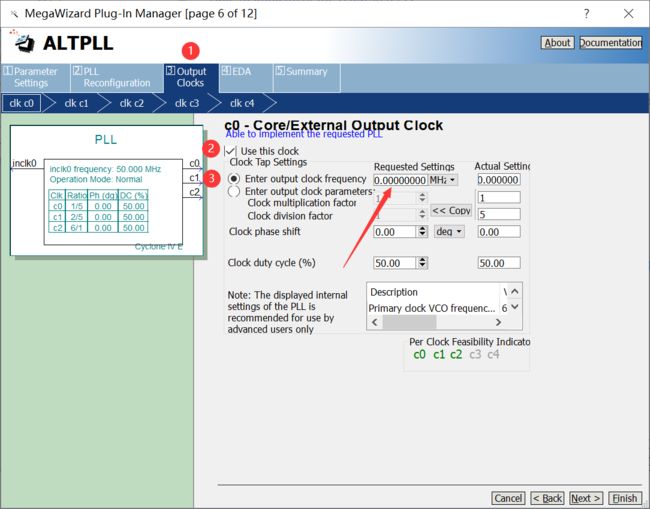
按照下列步骤配置输出的时钟频率,我这里配置了三个时钟clk c0、clk c1、clk c2,分别是10MHZ、20MHZ、300MHZ
生成文件,勾选生成对应的文件、我这里多勾选了bsf文件,是这个PLL ip核的波形文件、PLL_inst.v是实例化的部分,其他的文件这里不做过多的叙述

点击finish生成,这里生成了PLL的实现文件,我们可以将之前勾选的文件添加进项目中

生成的文件位置会在你创建项目的目录下,我们将PLL_inst初始化文件添加进来:

PLL_inst.v文件内容,会存放实例化模块,方便我们进行调用和仿真,我们只需要将我们的信号与PLL信号进行联通就行,如下列所示,c0将生成10MHZ的时钟、c1将生成20MHZ的时钟、c2将生成300MHZ的时钟
PLL	PLL_inst (
	.inclk0 ( inclk0_sig ),
	.c0 ( c0_sig ),
	.c1 ( c1_sig ),
	.c2 ( c2_sig )
	);
3、使用配置的PLL进行仿真
仿真代码:
// Copyright (C) 2018  Intel Corporation. All rights reserved.
// Your use of Intel Corporation's design tools, logic functions
// and other software and tools, and its AMPP partner logic
// functions, and any output files from any of the foregoing
// (including device programming or simulation files), and any
// associated documentation or information are expressly subject
// to the terms and conditions of the Intel Program License
// Subscription Agreement, the Intel Quartus Prime License Agreement,
// the Intel FPGA IP License Agreement, or other applicable license
// agreement, including, without limitation, that your use is for
// the sole purpose of programming logic devices manufactured by
// Intel and sold by Intel or its authorized distributors.  Please
// refer to the applicable agreement for further details.

// *****************************************************************************
// This file contains a Verilog test bench template that is freely editable to
// suit user's needs .Comments are provided in each section to help the user
// fill out necessary details.
// *****************************************************************************
// Generated on "07/24/2023 19:18:12"

// Verilog Test Bench template for design : t5
//
// Simulation tool : ModelSim-Altera (Verilog)
//

`timescale 1 ns/ 1 ns
module t5_vlg_tst();
// constants
// general purpose registers

// test vector input registers
parameter SYS_CLK = 20;
reg clk;

// wires
wire c0_sig;
wire c1_sig;
wire c2_sig;

// assign statements (if any)


always #(SYS_CLK/2) clk = ~clk;

initial begin
	clk = 1'b0;
	#(200*SYS_CLK);
	$stop;
end

PLL	PLL_inst (
	.inclk0 ( clk ),
	.c0 ( c0_sig ),
	.c1 ( c1_sig ),
	.c2 ( c2_sig )
	);

endmodule
4、仿真结果

我这里仿真了50MHZ的时钟,可以看到结果完全相符合
5、总结
在fpga开发中时钟配置十分重要,本文略讲的比较简单,可以观看下列视频加深了解
04_IP核之PLL使用讲解_哔哩哔哩_bilibili