【FPGA】7系列 FPGA时钟资源及时钟IP核配置 Xilinx
7系列 FPGA时钟资源及时钟IP核配置 Xilinx
7系列时钟资源
1.分类
全局时钟,区域时钟
2.7系列时钟结构

Clock Backbone:全局时钟线将芯片分成左右两个时钟区域;
Horizontal Center:水平时钟线将芯片分成多行时钟区域。
3.三个重要的时钟
BUFG:全局时钟,可以驱动整个芯片的IO和其他逻辑;
BUFR:区域时钟,一般只驱动各时钟区域的IO和其他逻辑;
BUFIO:IO时钟,只能驱动IO。
4.CMT
CMT,时钟管理单元。可以进行时钟管理,提供稳定的差频信号和倍频信号。包含PLL和MMCM两种模块,相较于PLL,MMCM功能更加强大,可以进行动态调整和反相。BUFR,BUFG,BUFH等都可以为PLL和MMCM提供时钟驱动。

5.Xilinx vivado 时钟IP核的使用
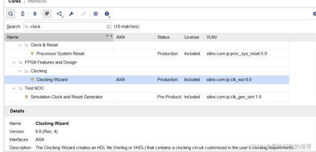
(1)点击左侧任务栏“IP Catalog”-搜索“clock”-双击“clocking wizard”
(2)参数设置:
器件名字:可以默认就可,或者自己设一个;
Clock Monitor:时钟监测器,选中后,会持续监测时钟的停止、时钟的故障和时钟的变化,我没用到就不勾选;
Primitive:选MMCM和PLL中的一个,前面简单介绍了两种的区别;
Clocking Features:时钟性能参数;
Frequency Synthesis:允许时钟输出不同的频率;
Phase Alignment:知道输入时钟的相位关系;
Dynamic Reconfig:动态时钟的调整,可以打开 AXI4或DRP;
Safe Clock Startup:输出时钟的延迟,在时钟稳定后再输出时钟;
Minimize Power:减少能耗;
Spread Spedrum:扩频;
Dynamic Phase Shift:允许输出时钟相位的动态改变;
JItter Optimization:抖动调整,分别为平衡,最小输出抖动和最大输入抖动过滤;

输入时钟设置Input Clock Information:将输入时钟修改与板卡一致,我是用的是50MHz的时钟,所以将第一个输入时钟频率修改为了50MHz;

输出时钟页:
我打算输出四个时钟,勾选四个,将四个输出时钟的频率(Output Frequence)修改为自己需要的,将四个时钟的相移(Phase)修改成需要的。
下面的需要使用的输入输出端口:
一般选择reset(复位端口)和locked(时钟稳定指示信号,时钟稳定时输出为高);
power down是开关,决定输出端口是否输出;
clkfpstopped:与反馈始终有关,反馈时钟丢失时,会给一个中断(不常用);
input_clk_stopped:输入时钟切换指示标志(不常用);
Reset Type:复位类型,一般是高电平有效(Active Low);

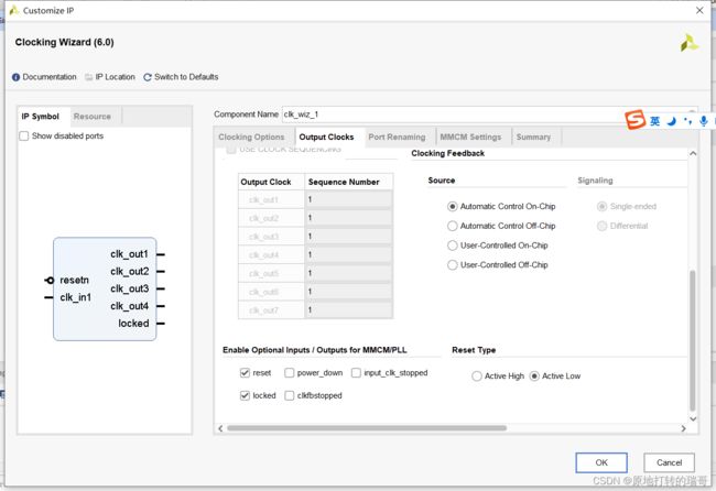
其他页是信息显示框,不用管;
点击OK-Generate生成时钟IP核-在IP Sourece中可以看到已经生成成功;
打开veo为后缀的文件-

直接在需要的模块中例化生成的时钟模块(如下)即可:

6.实例:
(1)生成的veo文件:
//
// (c) Copyright 2008 - 2013 Xilinx, Inc. All rights reserved.
//
// This file contains confidential and proprietary information
// of Xilinx, Inc. and is protected under U.S. and
// international copyright and other intellectual property
// laws.
//
// DISCLAIMER
// This disclaimer is not a license and does not grant any
// rights to the materials distributed herewith. Except as
// otherwise provided in a valid license issued to you by
// Xilinx, and to the maximum extent permitted by applicable
// law: (1) THESE MATERIALS ARE MADE AVAILABLE "AS IS" AND
// WITH ALL FAULTS, AND XILINX HEREBY DISCLAIMS ALL WARRANTIES
// AND CONDITIONS, EXPRESS, IMPLIED, OR STATUTORY, INCLUDING
// BUT NOT LIMITED TO WARRANTIES OF MERCHANTABILITY, NON-
// INFRINGEMENT, OR FITNESS FOR ANY PARTICULAR PURPOSE; and
// (2) Xilinx shall not be liable (whether in contract or tort,
// including negligence, or under any other theory of
// liability) for any loss or damage of any kind or nature
// related to, arising under or in connection with these
// materials, including for any direct, or any indirect,
// special, incidental, or consequential loss or damage
// (including loss of data, profits, goodwill, or any type of
// loss or damage suffered as a result of any action brought
// by a third party) even if such damage or loss was
// reasonably foreseeable or Xilinx had been advised of the
// possibility of the same.
//
// CRITICAL APPLICATIONS
// Xilinx products are not designed or intended to be fail-
// safe, or for use in any application requiring fail-safe
// performance, such as life-support or safety devices or
// systems, Class III medical devices, nuclear facilities,
// applications related to the deployment of airbags, or any
// other applications that could lead to death, personal
// injury, or severe property or environmental damage
// (individually and collectively, "Critical
// Applications"). Customer assumes the sole risk and
// liability of any use of Xilinx products in Critical
// Applications, subject only to applicable laws and
// regulations governing limitations on product liability.
//
// THIS COPYRIGHT NOTICE AND DISCLAIMER MUST BE RETAINED AS
// PART OF THIS FILE AT ALL TIMES.
//
//----------------------------------------------------------------------------
// User entered comments
//----------------------------------------------------------------------------
// None
//
//----------------------------------------------------------------------------
//  Output     Output      Phase    Duty Cycle   Pk-to-Pk     Phase
//   Clock     Freq (MHz)  (degrees)    (%)     Jitter (ps)  Error (ps)
//----------------------------------------------------------------------------
// clk_out1__100.00000______0.000______50.0______162.035____164.985
// clk_out2__50.00000______0.000______50.0______192.113____164.985
// clk_out3__50.00000____180.000______50.0______192.113____164.985
// clk_out4__25.00000______0.000______50.0______236.428____164.985
//
//----------------------------------------------------------------------------
// Input Clock   Freq (MHz)    Input Jitter (UI)
//----------------------------------------------------------------------------
// __primary______________50____________0.010

// The following must be inserted into your Verilog file for this
// core to be instantiated. Change the instance name and port connections
// (in parentheses) to your own signal names.

//----------- Begin Cut here for INSTANTIATION Template ---// INST_TAG

  clk_wiz_1 instance_name
   (
    // Clock out ports
    .clk_out1(clk_out1),     // output clk_out1
    .clk_out2(clk_out2),     // output clk_out2
    .clk_out3(clk_out3),     // output clk_out3
    .clk_out4(clk_out4),     // output clk_out4
    // Status and control signals
    .resetn(resetn), // input resetn
    .locked(locked),       // output locked
   // Clock in ports
    .clk_in1(clk_in1));      // input clk_in1
// INST_TAG_END ------ End INSTANTIATION Template ---------
(2)顶层调用模块:
module clk_ip(
    input           sys_clk     ,
    input           sys_rst_n   ,
    output          clk_100M       ,
    output          clk_50M        ,
    output          clk_50M_180    ,
    output          clk_25M        ,
    output          locked
    );

    clk_wiz_1 u_clk_wiz_1
    (
        // Clock out ports
        .clk_out1(clk_100M   ),     // 100M时钟
        .clk_out2(clk_50M    ),     // 50M时钟
        .clk_out3(clk_50M_180),     // 50M时钟,移相90度
        .clk_out4(clk_25M    ),     // 25M时钟
        // Status and control signals
        .resetn(sys_rst_n), // input resetn
        .locked(locked),       // output locked
        // Clock in ports
        .clk_in1(sys_clk)
        );      // input clk_in1
endmodule
(3)twstbench:
`timescale 1ns / 1ps
module tb_clk_ip(
    );
    reg  sys_clk    ;
    reg  sys_rst_n  ;
    wire clk_100M   ;
    wire clk_50M    ;
    wire clk_50M_180;
    wire clk_25M    ;
    wire locked     ;

    //激励信号产生
    initial begin
        sys_clk=1'b0;
        sys_rst_n=1'b0;
        #200 sys_rst_n=1'b1;
    end

    //时钟信号
    always #10 sys_clk=~sys_clk;

    //时钟IP模块的例化
    clk_ip u_clk_ip(
        .sys_clk        (sys_clk),
        .sys_rst_n      (sys_rst_n),
        .clk_100M       (clk_100M   ),
        .clk_50M        (clk_50M    ),
        .clk_50M_180    (clk_50M_180),
        .clk_25M        (clk_25M    ),
        .locked         (locked)
    );

endmodule
(4)结果:
