SCAU 数字电路 Digital Circuits and Logic Design 复习
ch2-1-1
Binary 二进制 Octal 八进制 Hexadecimal 十六进制
Number representation in radix r
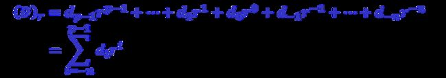
r: radix (基数)
ri: weight of digit di(权重)
dp-1: Most Significant Digit (MSD)
d-n: Least Significant Digit (LSD)
Binary Addition and Subtraction
里面有cout 和 cin 一般是指加法的进位,out是出去的,in进去的。bout 和 bin 则是减法的。
Number System Conversion
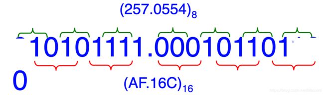
Binary to Octal/Hexadecimal
Partition the binary number into groups of three/four bits, starting at binary point and
integer part: going left
Fractional part: going right
Both the lefthand and righthand sides can be padded with ‘0’ if necessary
Each group corresponds to a single octal/hexadecimal digit.
从二进制点开始,将二进制数分成3/4位
整数部分:向左
分数部分:向右
如果需要,可以用“0”填充左侧和右侧
每组对应一个八进制/十六进制数字
ch2-2-1
Signed-Magnitude Representation (原码)SMR
The MSB position is 0 for positive numbers and 1 for negative numbers.
就是在符号位是1则是负数,是0则是正数,其他的位置不变。
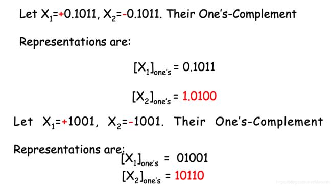
One’s Complement Representation (反码)OCR
Positive number: same as the positive SM numbers
Negative numbers: complement each bit of the SM of corresponding positive number including the sign bit
There are two representations of zero as well.
就是说正数的反码就是正数,负数的反码是对其原码逐位取反,但符号位除外。
Two’s Complement Representation (补码)TCRPositive number:same as its SMR and OCR.Negative number:add “1” to the one’s complement of the number. Only one representation to “0”.
正数依然不变,但是尼,负数则是反码加一。
为什么我们要搞那么多的码呢,因为计算机只会进行加法,不会进行减法,那怎么办呢。
比如5-8我们可以看作5+(-8),那不就可以看作一个加法了吗,所以就会出现补码这个东西,来表示-8。
Addition/Subtraction in TCR
[A+B]two’s=[A]two’s+[B]two’s
[A-B]two’s=[A]two’s-[B]two’s
Overflow
If the signs of the addends are the same but the sign of the sum is different, there is addition overflow.
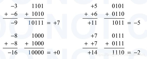
很明显可以看出,如果计算完后,符号位变了,则说明overflow了,并且,在计算过程中,多出的位是要直接舍弃的,比如上图中蓝色的一就是被舍弃的。
overflow的原因也很简单,就是结果超出了这个bit的承受范围。
Sign Extension
Two’s-complement number X:
(X)n-bit -----> (X)m-bit
Case 1: n > m. Discard the leftmost bits when they are the same as the sign bit.
Case 2: n < m. Append the sign bit to the left of X.
Exercise: (1011)two’s = (11111011)two’s
关键就是符号位啦。注意这是补码的extension噢,不是原码的,原码补0他不香吗。
Binary Codes for Decimal Numbers
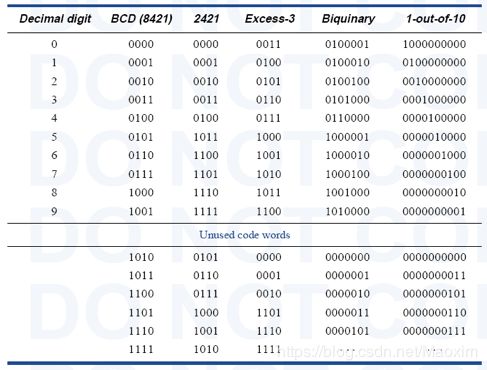
Binary-Coded Decimal (BCD, 8421)
例如0101 0110 代表86 每四位代表一个数字
2421 Code
A weighted code. (21, 22, 21, 20)
Self-complementing code for 9s’ complement.
就是以中心为轴,然后上下加起来,你会发现都为1111 (对9的自补码)
Excess-3 Code
Self-complementing code for 9s’ complement.
The corresponding BCD code plus 00112.
Follow a standard binary counting sequence.
Not weighted.
余三码,就是BCD码加个(0011)2
Gray Code
Only one bit changes between each pair of successive code words.
Reduce the chance of making mistakes via coding.
你会发现相邻两个code只有一个bit不同
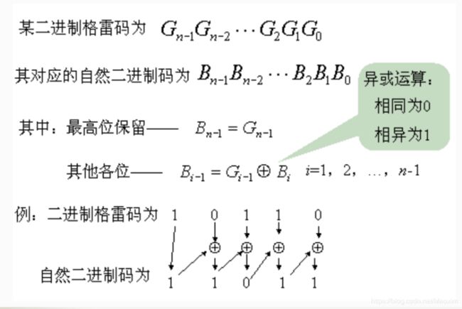
or
Gray code 的生成方法
ch 3
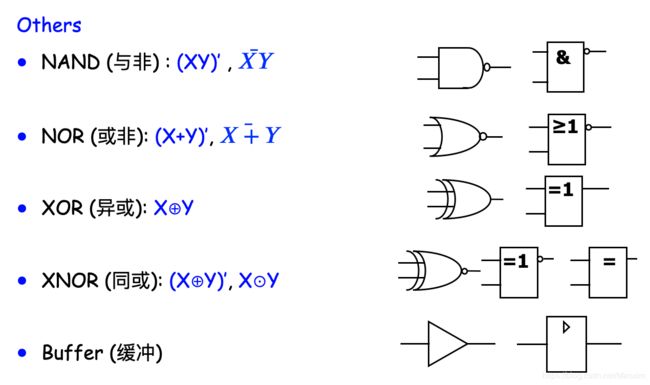
Logic Functions and Gates
AND (与门)
Function: Output 1 if and only if all of its inputs are 1 (输入有0,输出为0).
Expression: Z=A AND B; Z=A·B; Z=AB

OR (或门)
Function: Output 1 if and only if at least one of its inputs is 1 (输入有1,输出为1)
Expression: Z=A OR B; Z=A+B

NOT (非门, 反相器)
Function: Output a value that is opposite to the input value (输出对输入取反)
Expression: Z=NOT A; Z=A’; Z= Ā

CMOS Logic
Positive logic (正逻辑) and Negative logic (负逻辑)
Positive logic: assigning 0 to low and 1 to high
Negative logic: assigning 1 to low and 0 to high
Logic Family:
Bipolar junction transistor circuits: TTL, ECL
MOS transistor circuits: NMOS, PMOS, CMOS
CMOS is the most commonly used logic family.
MOS Transistors
Principle: The gate voltage creates an electric field that enhances or retards the flow of current between source and drain.
也就是根据输入的gate,来判断drain和source是否连接
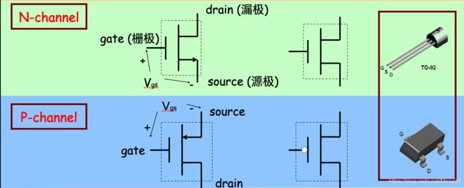
当N-channel的gate为1的时候,drain和source连通(接地)
当P-channel的gate为0的时候,drain和source连通(接高电压)
反之则不连通
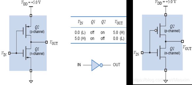
CMOS Static Electrical Behavior
1.Logic Levels and Noise Margins (逻辑电平和噪声容限)
VILmax: when the range of input voltage is between ground and VILmax, recognized as the low by input.
VIHmin: when the range of input voltage is between Vcc and VIHmin, recognized as the high by input.
VOLmax: when output in the low state, Vout: 0~VOLmax.
VOHmin: when output in the high state, Vout: VOHmin~Vcc.
也就是说,低电压是指0-2.4(0),高电压是指2.6-5(1)
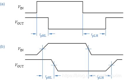
2.Propagation delay (传输延迟): tp
tpHL: the time required for the output to change from HIGH to LOW caused by input change.
tpLH: the time required for the output to change from LOW to HIGH caused by input change.
3.Power consumption (功耗)
When output is not changing, the power consumption --> static power dissipation is very low.
When output experiences transitions, the power consumption --> dynamic power dissipation is high, and the transition frequency is the primary reason.
ch 4
Combinational logic circuit
Outputs depend only on its current inputs, e.g. 1-bit addition.
No feedback loops.
Sequential logic circuit
Outputs depend on the current inputs and current states.
With feedback loops.

Switching Algebra: Axiom (公理)
(A1) if X≠1, then X=0;
(A1’) if X≠0, then X=1
(A2) if X=0, then X’=1;
(A2’) if X=1, then X’=0
(A3) 0·0=0 (A3’) 1+1=1
(A4) 1·1=1 (A4’) 0+0=0
(A5) 0·1=1·0=0 (A5’) 0+1=1+0=1
(T1 T1’) 0-1律: X+0=X; X· 1=X
(T2 T2’): X+1=1; X· 0=0
(T6 T6’) 交换律: X+Y=Y+X; X·Y=Y·X
(T7 T7’) 结合律: (X+Y)+Z=X+(Y+Z); (X· Y)· Z=X·(Y· Z)
(T8 T8’) 分配律: X· (Y+Z)=XY+XZ; “multiply out for SOP form”
X+YZ=(X+Y)· (X+Z); “add out for POS form”
(T3 T3’) 重叠律: X+X=X X· X=X
(T4) 还原律: (X’)’=X
(T5 T5’) 互补律: X+X’=1; X· X’=0
(T9 T9’) 吸收律: X+XY=X; X· (X+Y)=X;
X+X’Y=X+Y; X(X’+Y)=XY
(T10 T10’) 合并律: XY+XY’=X; (X+Y)· (X+Y’)=X
(T11 T11’) 包含律: XY+X’Z+YZ=XY+X’Z
(X+Y)· (X’+Z)· (Y+Z)=(X+Y)· (X’+Z)
Switching Algebra: Regulation (规则)
Duality (对偶规则)
A Boolean equation remains valid if we take the dual of the expressions on both sides of the equal sign.
F1=F2 <—> F1D=F2D (两逻辑式相等,则其对偶式也相等)
The dual of an algebraic expression is obtained by OR<—>AND, 0<—>1.
简单来说就是:符号改变,0和1互换,变量不变
Generalized Demorgan’s theorem (反演规则)
Given a logic expression F, its complement can be obtained by taking the dual of the logic expression and complementing each variable.
[F(x1,x2,…,xn)]’ = FD(x1’, x2’,…,xn’)
就是说对偶后对变量去反就是反演

这个可以用来化简电路图,例如抵消取反
Standard Representations of Logic Functions
Canonical sum (标准和) : the sum of the minterms that produces a 1 output in truth table.
需要注意的就是,例如xyz对应的就是111,x‘y’z‘对应的就是000
Canonical product (标准积) : product of the maxterms that produces a 0 output in truth table.
需要注意的就是,例如xyz对应的就是000,x‘y’z‘对应的就是111
For a logic function, it can be expressed by canonical sum or by canonical product. The number list of each belongs to two complement sets.
mi=Mi’.
∑ and ∏ with same list are complement of each other.互补
There are 6 descriptions for a combinational logic circuit.
Combinational Circuit Minimization
Algebra Method (代数法)
Apply axioms, theorems and regulations of switching algebra directly on logic expressions.
No limitation on the number of variables.
Not easy to accomplish by computer.
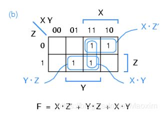
Karnaugh Maps (卡诺图)
A pictorial form of truth table.
n-variable K-Map: a map with 2n square cell; each cell corresponding to a minterm and its output value in truth table.
Adjacent logically (逻辑相邻): minterms differ in only one variable.
When 2n minterms are adjacent logically, the sum of these minterms can be simplified to a single product term after removal of the n different variables.
Make adjacent cells in K-Map differ in only one variable, and turn “adjacent logically” into “adjacent positionally”.
Don’t Care (无关项)
Some input combinations are forbidden (约束项).
The outputs don’t matter when some input combinations occur (任意项).
Rules:
Don’t circle “d” alone.
Cover those “d” which can make the circle as large as possible.
Timing Hazards (定时冒险)
Circuit delay:
The transient behavior of a combinational logic circuit may differ from what is predicted by a steady-state analysis.
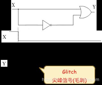
Static-1 Hazards (静态-1冒险)
A circuit’s output may produce a 0 glitch when it should remain 1 based on a static analysis.
How to judge?
In expression: F=X+X’ can appear finally.
In K-Map: Two circles are “tangent”.
Elimination:
Add circles to cover those “tangent” minterms in K-Map.
就是把相切的卡罗圈接起来
Static-0 Hazards(静态-0冒险)
Be treated “duality” with static-1 hazards.
ch 6
Several Structures
Decoder(译码器)
Encoder(编码器)
Multiplexer(多路复用器)
Parity circuits(奇偶校验电路)
Comparator(比较器)
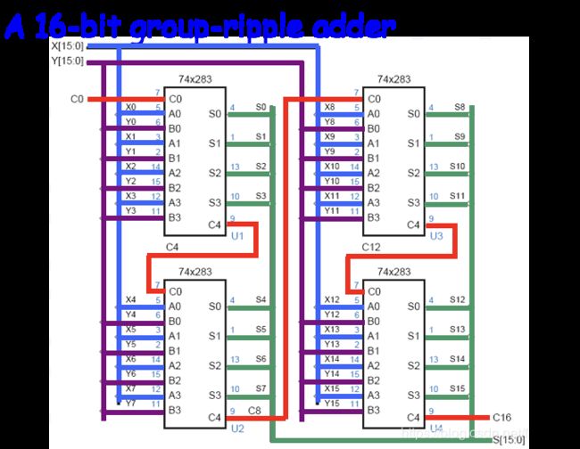
Adder(加法器)
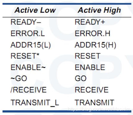
Active Levels
就是分高电频有效和低电频有效
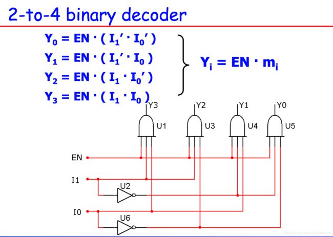
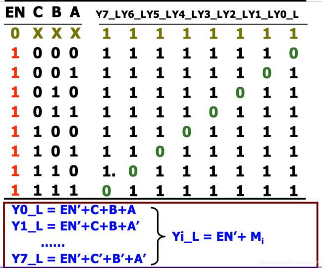
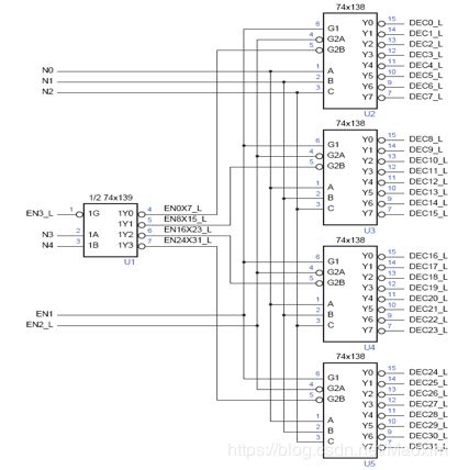
Decoder-译码器 Binary decoders (二进制译码器) Such as 2 to 4 binary decoder MSI: Dual 2-4 binary decoder 74×139 3-8 binary decoder MSI:3-8 binary decoder 74x138 Design 4-16 decoder using 74x138 BCD Decoder (BCD 译码器) Priority Encoders (优先级编码器) Multiplexers (多路复用器MUX) MUX-DEMUX Application Multiplexers Expanding Multiplexers Implement the Combinational Circuits Demultiplexer (多路分配器, DEMUX) Magnitude Comparators (数值比较器) MSI: 74x682 (8-bit 数值比较器) A 12-bit comparator using 74x85s Adders (加法器) Carry-lookahead Adders (先行进位加法器) A 16-bit group-ripple adder Combinational logic circuit State memory: The state memory is a set of n flip-flops that store the current state of the machine, and has 2n distinct states. Sequential circuits are sometimes called Finite-State Machine (有限状态机) Clocked synchronous state machine Latches and Flip-Flops (锁存器与触发器) S-R Latch Characteristic Equation Minimum Pulse Width (最小脉冲宽度) S’-R’ Latch S-R Latch with Enable Timing Diagram Edge-triggered D Flip-Flop (边沿触发式D触发器) Clocked Synchronous State-Machine Analysis Clocked Synchronous State-Machine Design 这个同理,具体的需要自己练习,下面说下需要注意的点: Design a “1111” sequence detector (序列检测器) State Minimization
Multiple-input, multiple-output combinational logic circuit
For n-bit input combinations, get the m-bit output combinations with one-to-one mapping when the enables are asserted (n
Input: n-bit binary code
Output: 2n-bit,for each input combination, only one of 2n is asserted (1-out-of-2n)
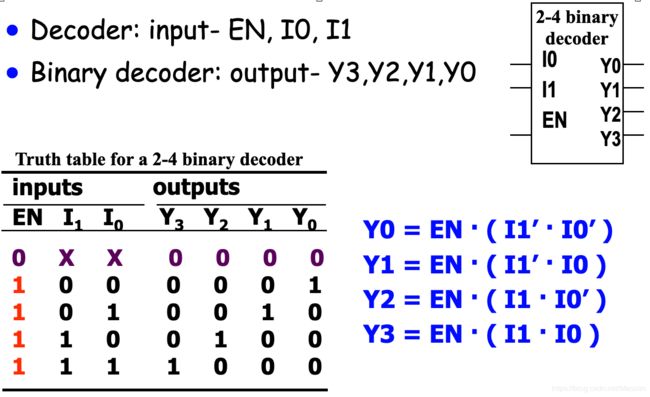
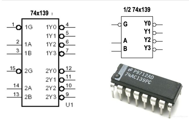
这个就是双处理的,就是可以处理两个的数
其中1G和2G是EN端 1A1B 2A2B则是输入端,分别代表两个数
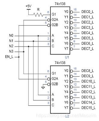
3-8 binary decoder truth table
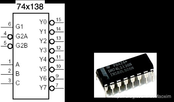
Inputs:N3N2N1N0
Outputs:DEC0_L~DEC15_L
N2N1N0 are inputs of two 74x138,N3 is Enable
N3=0, U1 Enable, decode 0~7
N3=1, U2 Enable, decode 8~15
EN_L is Enable of 4-to-16 decoder
就是把两个通过EN端连接起来
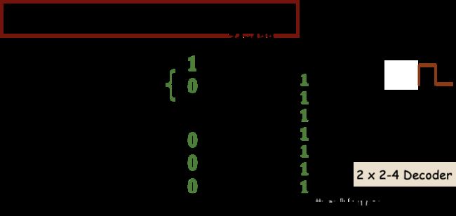
5-to-32 Decoder
Applications of Binary Decoder
Binary decoder can be used as minterm or maxterm generator.
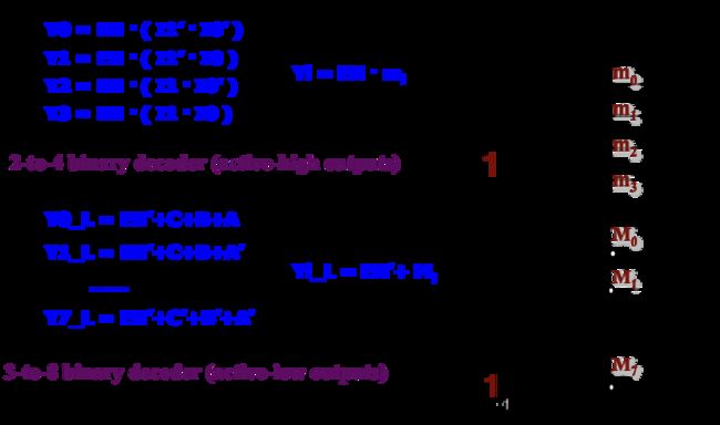
eg:
F = ∑X,Y,Z(0,1,4,6,7)
F = ∑A,B,C,D,E(1,3,5,7,19,21,23)
= A’B’C’D’E + A’B’C’DE + A’B’CD’E + A’B’CDE
+ AB’C’DE + AB’CD’E + AB’CDE
= B’E(A’C’D’ + A’C’D + A’CD’ + A’CD + AC’D + ACD’ + ACD)
= B’E(m0 + m1 + m2 + m3 + m5 + m6 + m7)
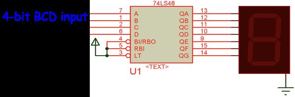
Inputs: 4-bit BCD code
Outputs: 1-out-of-10
二-十进制译码器,十进制译码器
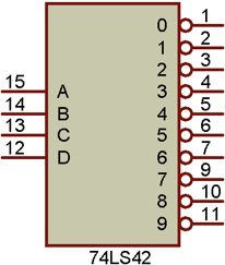
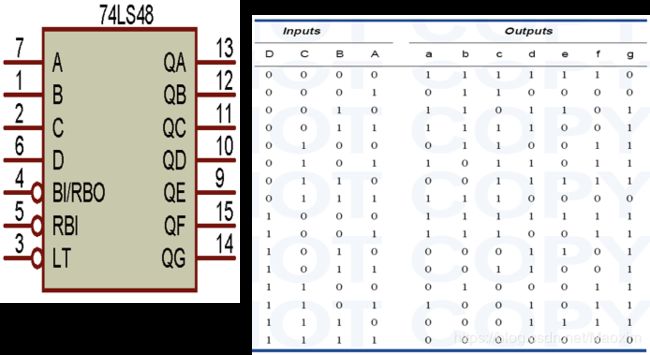
这里的truth table我看了很久,后来才发现,原来其abcdefg的含义居然是代表的位置
具体如下:
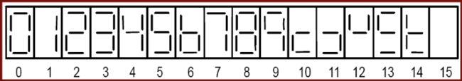
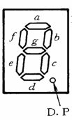
你会发现像这种数字可以由7个横线构成,也就是说,可以由output组成,总而言之,这个decoder的作用就是把二进制转化为(可视)的十进制。
Binary Encoder
8-3 Binary Encoder
A 2n-to-n encoder can be built from n 2n-1-input OR gates. Bit i of the input code is connected to OR gate j if bit j in the binary representation of i is 1
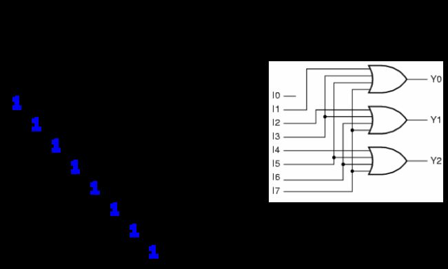
这样来说,I7的优先级是最大的,比如I7为1,则其他的都要为0
像优先级编码器就是用来处理这种十进制转二进制的。
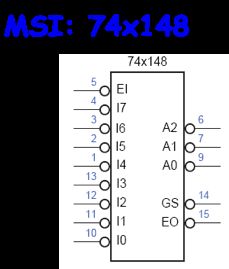
EI_L: Enable Input
EO_L: Enable Output, is asserted when EI_L is asserted and no inputs are asserted.
GS_L: Group Selection, is asserted when EI_L is asserted and at least one input is asserted.
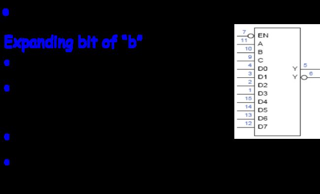
MUX uses the control inputs to select one of the data inputs and connects it to the output terminal.
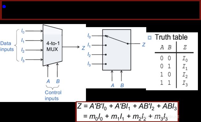
简单来说,就是输入一个二进制AB,然后从I0到I3中选一个输出。
Inputs:n sources; b-bit per source; s-bit select, n =2s; Enable.
Outputs:one of n sources (b-bit)
8-input, 1-bit MUX
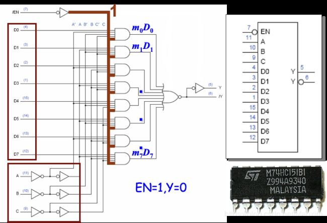
1bit是指输出一个
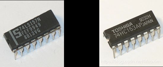
74x157: 2-input, 4-bit MUX
74x153: 4-input, 2-bit MUX
也就是需要16个74x151
Base: Y=∑miDi
Y=∑X,Y,Z(1,3,5,6)
=m1+m3+m5+m6
=m0·0+m1·1+m2·0+m3·1+m4·0+m5·1+m6·1+m7·0
Y=∑A,B,C,D(0,1,3,7,9,13,14)
=A’B’C’D’+A’B’C’D+A’B’CD+A’BCD+AB’C’D+ABC’D+ABCD’
=m0·1+m1·D+m2·0+m3·D+m4·D+m5·0+m6·D+m7·D’
也就是说这个可以应用到标准和中
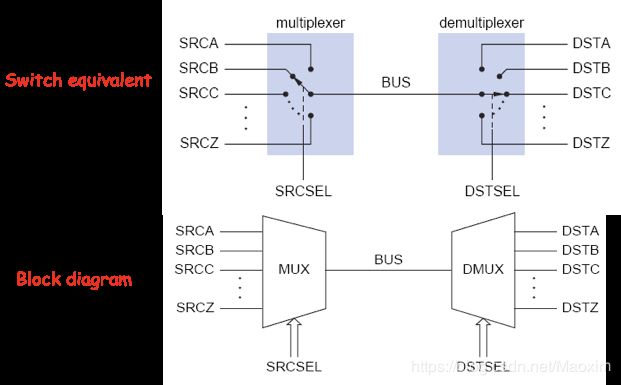
A binary decoder with enable can be used as a DEMUX.
The decoder’s enable input is the data input.
就是说binary decoder可以用作DEMUX
Comparators
A circuit that compares two binary words and indicates whether they are equal.
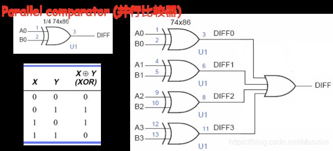
Iterative Comparator (迭代比较器)
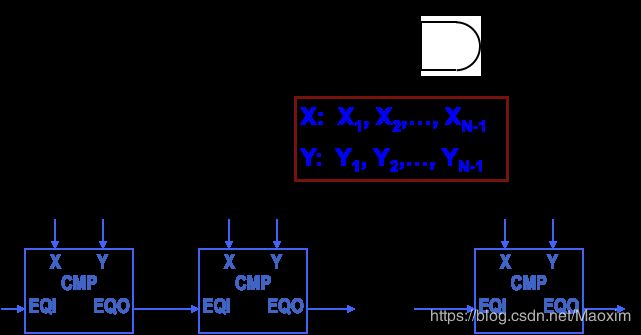
Ripple from the leftmost to the rightmost module.
Use EQi to keep track of whether all of the bit-pairs have been equal so far.
就是说,因为这个只能比一个bit,但如果我们相比较一个多位数的时候,我们就可以迭代去比,就行1234和1243比较的话,就是比较每一个数是否相同,这个比较器也是同理。
Inputs:1-bit binary number A, B
Outputs:YA>B, YA=B, YA
刚刚是比是否相同,这个是比谁大谁小
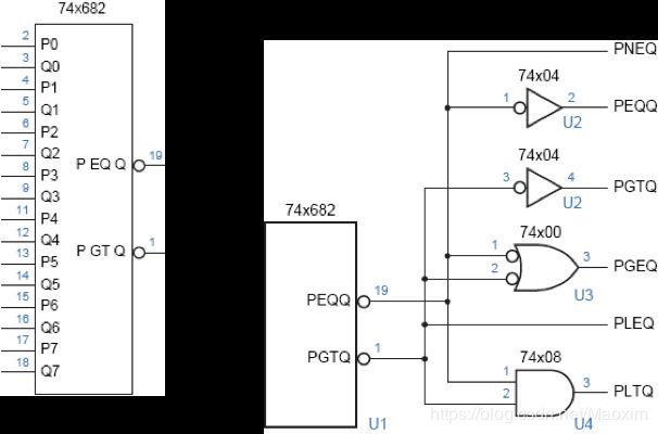
MSI: 74x85 (4-bit 数值比较器)
ALTBOUT=(A
AGTBOUT=(A>B)+(A=B)▪AGTBIN
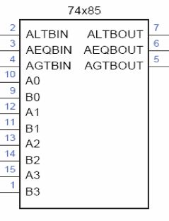
这里面的ALTBIN,AEQBIN和AGTBIN是用来记录比它高位的情况,也就是迭代时候用的。
就好像90001块钱和88889块钱,只要最开始的9比8大,那就是更有钱,后面的都不想看了。
ALTBOUT=(A
AGTBOUT=(A>B)+(A=B)▪AGTBIN
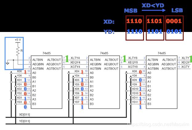
这个就是利用了迭代的思想
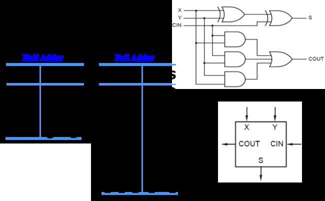
1-bit Half Adder
1-bit Full Adder
加法器有两种,一种就是加了后不告诉你有没有进位,另一种就是告诉你
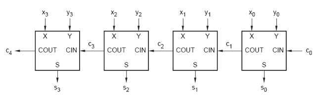
Ripple Adders (逐位(串行)进位加法器)
这个很慢,因为c4要等c3,c3要等c2·······
Cout=XY+CinX+CinY
c1=g0+p0▪c0
c2=g1+p1▪c1
=g1+p1▪(g0+p0▪c0)
=g1+p1g0+p1p0c0
gi=xiyi pi=xi+yi
这个就不能等,可以直接从公式推出来每个cout
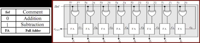
Application: Full Subtractor from Full Adder
Truth table of the 1-bit Full Subtractor
X, Y are n-bit unsigned binary numbers
Addition: S = X + Y
Subtraction: D = X - Y
= X+ (Two’s Complement of Y)
= X+ (One’s Complement of Y) + 1
= X+ Y’+ 1
加减法都能算
ch7
Outputs depend only on its current inputs
No feedback loops
Sequential logic circuit
Outputs depend on the current inputs and the past inputs (past inputs → current states)
Contain state memory (状态存储器).
A state memory can store one bit of information.
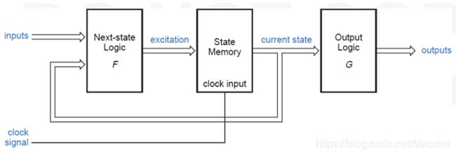
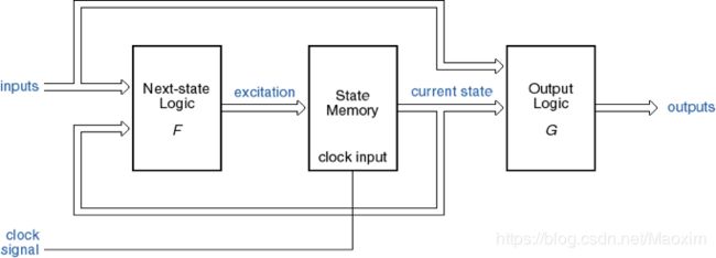
Next-state logic: as a function of the current state and input.
Next state = F(current state, input)
Output logic: as a function of the current state and input.
Output = G(current state, input)
Clocked synchronous state machine(时钟同步状态机):the circuit is controlled by a clock signal.
Mealy (米里机): A sequential circuit whose outputs depends on both states and inputs.
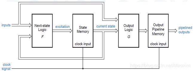
Moore (摩尔机): A sequential circuit whose outputs depends on the states alone.
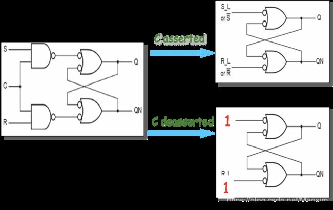
Bistable Device (双稳态元件)
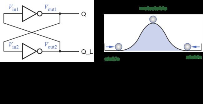
就是说如果Q=Q_L的话是处于亚稳态,一般是不会出现这种情况,因为不稳定。
所以默认情况下Q=(Q_L)’
Both are bistable device, and can serve as state memory.
Latch(锁存器): can change its outputs at any time when its enable is asserted.
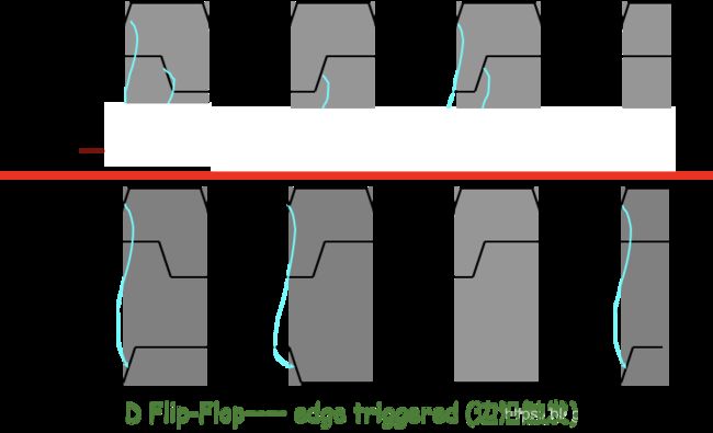
Flip-Flop(触发器): samples its inputs and changes its outputs at each tick of the clock.
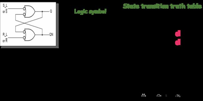
S: SET (置位) 就是置位为1
R: RESET (复位) 就是复位为0
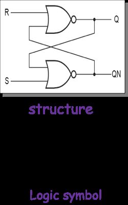
就是当S为1的时候S起作用 R为1的时候R起作用
两个相等的时候则是亚稳定的状态,所以一般不允许S和R同时为1
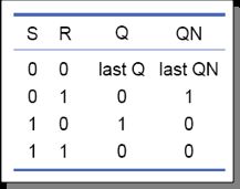
when S=0, R=0, If current state Q=QN’, hold the last state.
Q* = S + R’·Q under SR=0
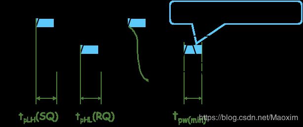
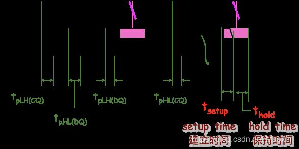
Propagation delay:the time it takes for a transition on an input signal to produce a transition on an output signal.
The latch may go into the metastable state if a pulse shorter than the tpw(min).
说白了就是超过蓝色那一段
Q* = S + R’·Q under SR=0
D Latch
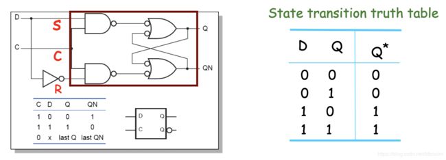
C asserted:transparent
C negated:hold last value
Characteristic equation:Q* = D
就是这个电流变化怎么画
这里需要注意的是,D触发器就是会有输入D,T触发器则会有输入T
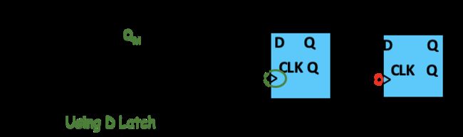

D Latch – Level Enable (电平有效)
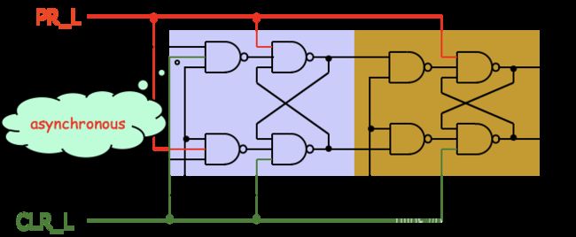
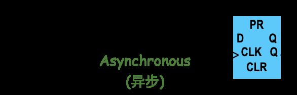
D-FF with PR and CLR
perset 就是吧Q重置为1 , clear就是把Q重置为0
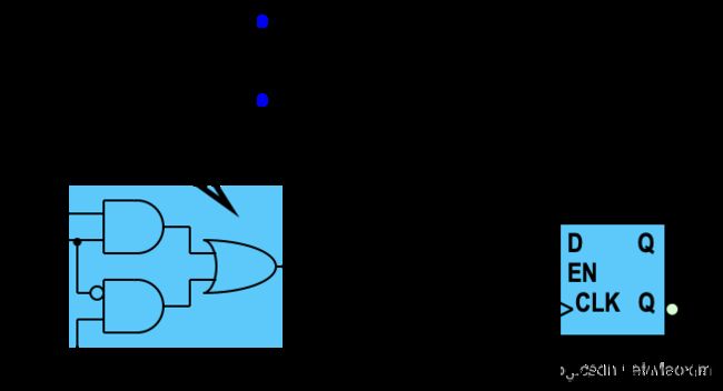
Edge-Triggered D FF with Enable
这个就是D触发器多了一个EN端
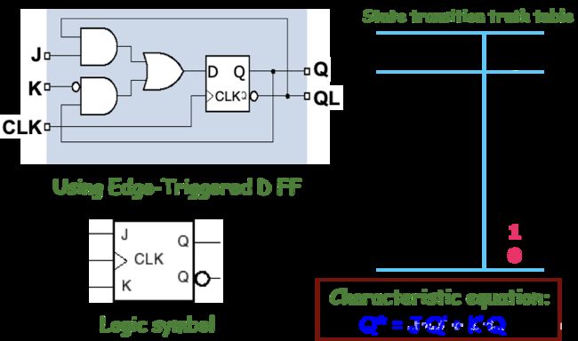
Edge-Triggered J-K Flip-Flop (边沿J-K触发器)
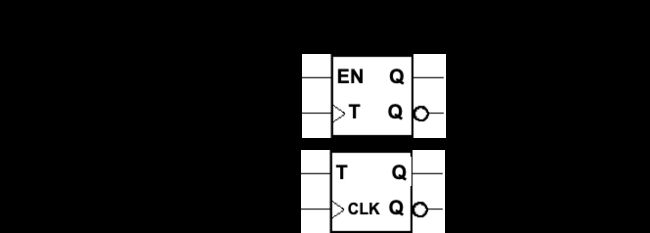
T Flip-Flop
每上升一次或者下降一次就改变一次。
注意区分D触发器和F触发器
Implementation of T’ FF
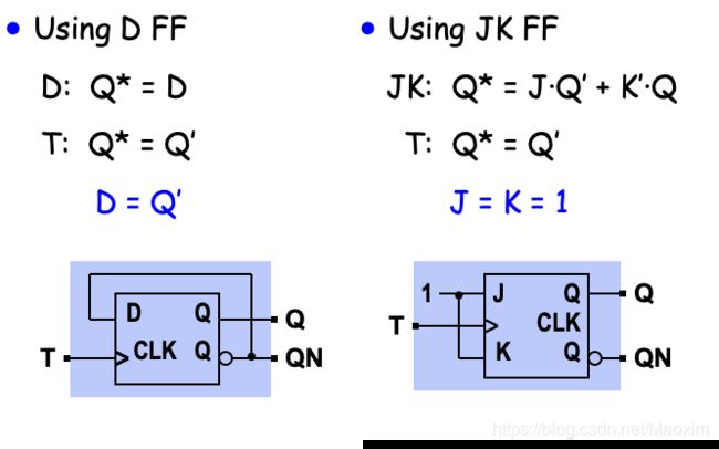
Implementation of T FF
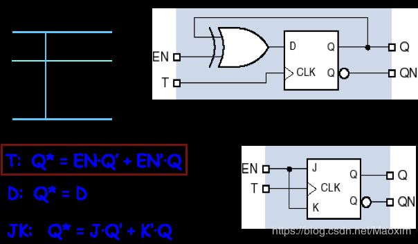
总结下公式
D-FF Q*=D
JK-FF Q*=JQ’+K’Q
T-FF Q*=EN异或Q

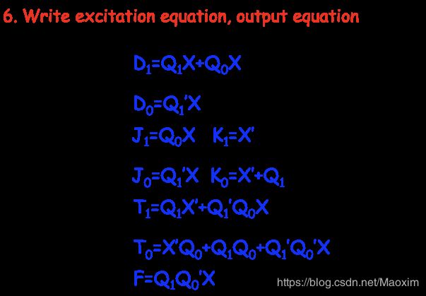
1.1: write the excitation equation from the logic diagram
1.2: write the transition equation
1.3: write the output equation
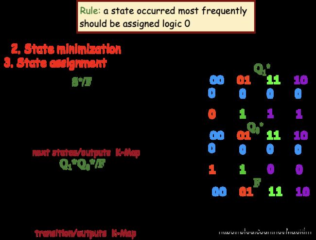
2.1: create transition/output table
2.2: create state/output table
3: Draw state diagram/Timing diagram
记住分析的步骤,一步步来
例子啥的就看书吧,说也说不清。过程比较复杂,考试时间短,需要提高下速度哦
Steps: Determine inputs, outputs.
if using D-FF, equal to transition/output table
if using JK-FF or T-FF, through application table (应用表)
下面就是根据问题自己来设计了!
下面给一个例子,具体的和之前讲的一样


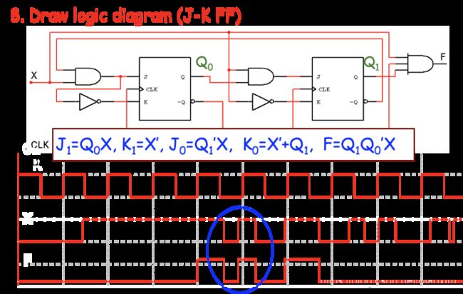
注意重要的一点:mealy会提前输出一个CLK,别问,问就是自己想
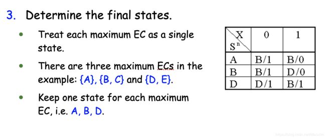
The state diagram in the first step may not be minimum and may contain redundant states.
The number of FFs depends on that of states.
It is necessary to minimize the state diagram to reduce the number of FFs and gates.
Reduce redundant states from the original state diagram, to get a minimized diagram.
就是化简
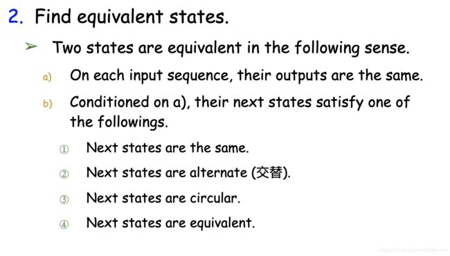
If for each input sequence, states S1 and S2 share exactly the same next state, we say S1 and S2 are equivalent, denoted by (S1, S2), or states S1 and S2 are an equivalent pair.
The input sequence here could be of arbitrary length and combination.
Transferability: (S1, S2), (S2, S3) --》 (S1, S2, S3)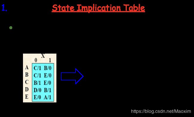
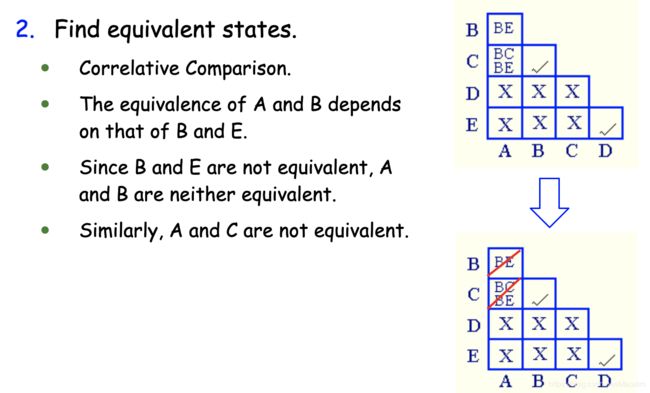
下面说下这个需要注意的点:
一般计数的时候不需要化简
化简的作用是啥子呢,就是可以少一个状态,少一个触发器,对地球妈妈多一点爱
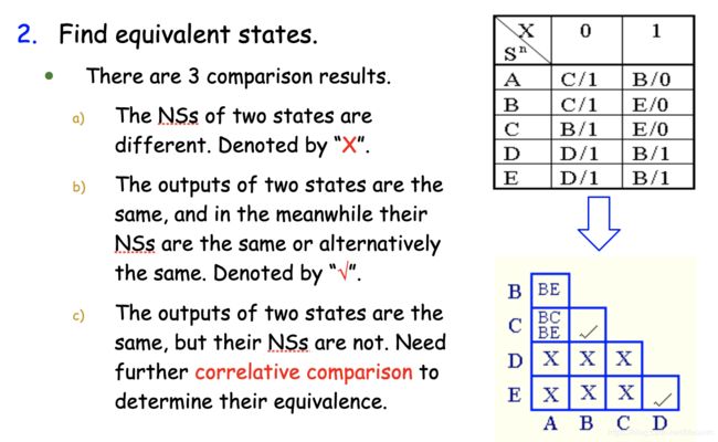
如何判断一不一样呢,就是末状态和输出需要一致,如过两个相互照应也是可以的哦
我们先看输入,输出不一样的时候直接pass
记得画个三角形,考试的时候,最后记得把化简后的表给画出来,要不然,你就是憨憨
对了,还要说明下,谁和谁是一对的。
例如From the comparison we get 5 maximum ECs, i.e. {A, E}, {B, F}, {C}, {D} and {G}. Then we have the final state diagram as follows.