Fully Digital Implemented Delta-Sigma Analog to Digital Converter
http://www.design-reuse.com/articles/14886/fully-digital-implemented-delta-sigma-analog-to-digital-converter.html
by Dr. Michael Gude & Gerriet Mueller
Cologne Chip AG, Koeln (Cologne), Germany
Abstract
One of the most challenging tasks in Analog to Digital Converter (ADC) design is to adapt the cicuitry to ever new CMOS process technology. For digital circuits the number of gates per square mm app. doubles per chip generation. Integration of analog parts in newer deep submicron technologies is much more tough and additionally complicated because the usable voltage ranges are decreasing with every new integration step.
This paper shows an approach which only uses 2 resistors and 1 capacitor which are located outside a pure digital chip. So all integration advantages of pure digital chips are preserved, there is no design effort for a new chip generation and the ADC also can be used for FPGAs. Measurement results of a first implementation show a resolution suitable for G.712 voice codecs for telecommunication. With additional effort resolutions of up to 16 bit are achievable. Sample rates in the 1 MHz region are feasible so that the approach is also useful for ADCs for xDSL technologies.
1. Introduction
Analog to Digital Converters (ADCs) are a widely needed and used circuitry in todays semiconductor chips. They convert an analog input signal to a proportional digital value, normally represented by a number of bits as binary number. Main properties of an ADC is the number of bits commonly named “resolution” and the speed of the ADC normally measured in samples per second.
One big group of ADCs are delta-sigma ADCs. They implement an oversampling approach which uses e.g. an integrator and a 1 bit ADC with a much higher sampling frequency of the analog input voltage than the achieved multi-bit output rate. Digital circuitries composed of filters and decimation logic then convert the high speed 1 bit signal into a multi-bit signal with lower frequency. If a 1 bit converter is used the analog circuitry is very much simplified and many parameters of the chip manufacturing process does not or only slightly influence the quality of the ADC. Furthermore a big portion of the ADC can be realized in pure digital logic which can be reduced in size with every new chip generation.
Even if the analog portion of a delta-sigma type ADC is small, one of the most challenging tasks in ADC design is to adapt the circuitry to ever new CMOS process technology. For pure digital circuits the integration advantage is app. a factor of 2 per integration step. So the number of gates per square mm doubles for each new chip generation.
Integration of analog parts is much more tough. In state of the art deep submicron technologies it is additionally complicated because the voltage ranges which can be used in the core area are decreasing with every chip generation.
2. Simple first order Delta-Sigma ADC
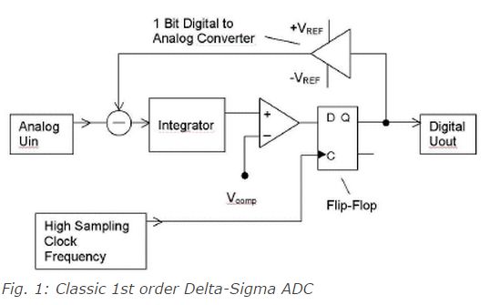
Fig. 1 shows a normal delta-sigma converter of first order. The most important analog components are a voltage integrator, a reference voltage source and a voltage comparator which in fact is a one bit ADC. This structure can be simplified as shown in Fig. 2. The integrator is replaced by a simple capacitor, the voltage adder is replaced by 2 resistors, the comparator is replaced by an input buffer of a pure digital chip and the voltage reference is replaced by the supply voltage of the chip
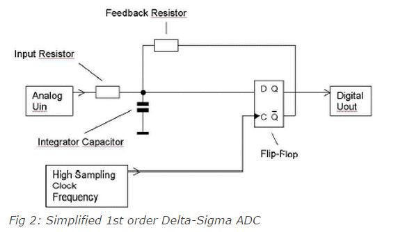
This approach is already known [1] but the performance is poor. You can achieve only a resolution of app. 7 bits [1]. The benefit of the structure is that it is easy to achieve a high oversampling frequency because there is no switched capacitor integrator used.
3. Improvements to achieve high resolution
The RC integrator which replaces the integrator has many advantages compared with a traditional switched capacitor approach with amplifier. As described in [2] the integrator must meet special requirements. This is mainly a speed and an accuracy requirement. Furthermore the integrator needs some chip area and supply current for the amplifier.
In contrast to this the RC integrator has nearly no negative parasitic disadvantages. It does not consume any additional supply current. The accuracy is only limited by the very small noise level of resistor and capacitor. Externally of the chip an absolute accuracy of better then 1% is of very low cost. However in voice or xDSL applications the absolute accuracy of the ADC is even not a key feature.
The exact time constant of the RC element is even not critical if the voltage swing on the capacitor is kept small. Because the input voltage also goes through a resistor the input voltage range can be much higher than the supply voltage of the digital chip. The up to now known poor quality of this ADC can be overcame by improving two things:
a) Accuracy of comparator threshold voltage
b) Accuracy of feed back output voltage
3.1 Accuracy of comparator threshold voltage
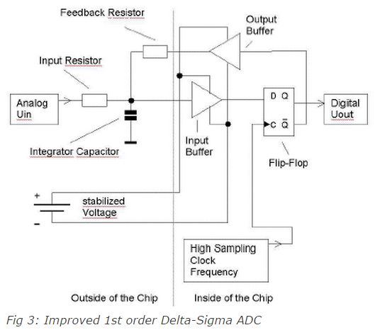
The accuracy of the input threshold voltage of the comparator which is now replaced by a simple input buffer is mainly influenced by noise on the supply voltage of the buffer. This is due to the fact that the threshold voltage for a normal input buffer is a share of the supply voltage. The noise can easily be reduced if the supply voltage connections of the buffer are routed to special power pads to feed the buffer with a special low noise voltage or a noise reduction for the buffer is implemented on chip.
Furthermore a normal CMOS type digital input buffer should be modified so that the supply current is reduced. Because the buffer is operated at the digital switching level (normally Vdd/2) a normal digital buffer would draw a big current from the supply. By using smaller transistors the current can be reduced dramatically only leading to a reasonable increase in the delay characteristics of the buffer. As shown below the delay time is normally not a critical value, sometimes a bigger delay in the feedback path is even wanted.
Most important is that even the accuracy of the “comparator” is not a key feature for first order delta-sigma ADCs. In [3] it is even recommended to add a noise source with well known characteristics to the comparator level to avoid long cyclic patterns in the digital output.
3.2. Accuracy of feed back output voltage
Unfortunately noise and inaccuracy of the reference voltage directly influences the performance of the ADC. So if we use the supply voltage instead a specially stabilized reference voltage source automatically the performance of the ADC is decreased. Here the output buffer of the digital chip is responsible for the connection to the supply voltage. By using additional power pads for this output buffer which are feed by a noise reduced stabilized voltage or an internally on chip stabilized voltage the performance of the ADC can be increased.
In many cases even a good blocked and decoupled supply voltage is already sufficient. Noise portions which come from the sampling frequency or even multiples of it are not influencing the performance of the ADC. This is due to the fact that all integer multiples of the clock frequency influence each output pulse of the ADC in the same way. So the effect is the same as if the output voltage is permanently changed by a small amount. For voice codecs also very low frequencies and the exact scaling of the ADC are no key aspects.
4. Reducing of output frequency
Because the resolution increase compared with the oversampling ratio for a first order delta-sigma ADC is only 9db/octave [4] the oversampling ratio for a 78dB voice codec ADC should be at least 9 octaves which means a sample clock frequency ratio of 512 / 1. For a sample clock of 8 kHz this means a high sampling clock for the converter of 4 MHz. This can be easily achieved. To reduce effects of EMI and reduce the power consumption of the ADC it is useful to implement some means to reduce the maximum feedback frequency going out of the output buffer. This does not significantly reduce the resolution of the ADC because the feedback pulses are limited in frequency but the time resolution of the pulses is preserved.
4.1 Dimensioning of RC characteristics
The easiest way to reduce the output frequency is to dimension the external RC time constant in a way that the feedback path needs more than one sample clock to compensate for an output voltage change. This is not always the best way because the gain of the input buffer should be as high as possible to have a small voltage swing on the capacitor. So a big time constant of the RC feedback leads to a very noise sensitive input. Furthermore the frequency can be limited if additional delay is implemented in the loop.
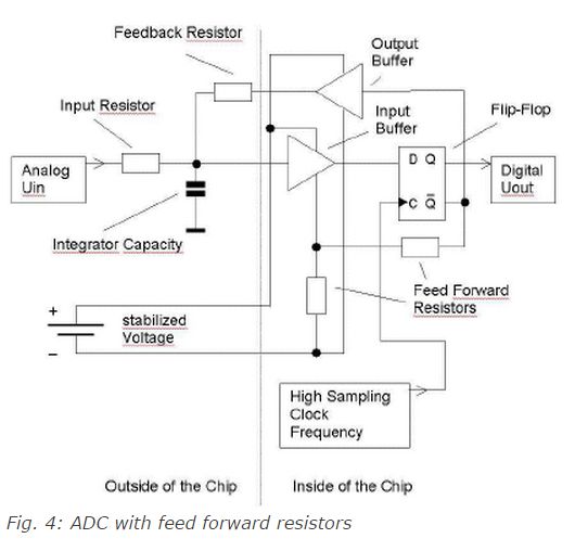
4.2. Using feed forward
As shown in Fig. 4 a small internal feed forward can be used. This leads to a small hysteresis in the input path to the flip-flop. This small feed forward can be generated by a small change in the switching point of the input buffer as shown in Fig. 4.
5. Filter and decimator
Using small voltage swings on the capacitor (e.g. app. 20-50mV for a 3.3V LVCMOS type input buffer) result in an integrator characteristic which is nearly identical to a real integrator. So for the above mentioned 78dB ADC no special precautions or changes must be made to the decimator and filters compared to a traditional delta-sigma type ADC. This preserves the ability to use well known filter/decimator circuitries as used for traditional delta-sigma type ADCs.
6. Measurement results
As a first implementation of the here described DIGICCTM (Digital codec by Cologne Chip) technology a G.712 PCM voice codec was designed. Fig. 5 shows measurement results even of a FPGA implementation with external buffer in the input and in the output path. These were used because the FPGA did not offer separated power connections and low hysteresis for the buffers.
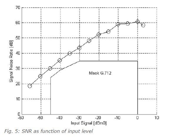
The mask in Fig. 5 is according to Figure 12 in G.712 [5] as a requirement from analog E4in to digital Tout. The signal representation in Fig. 5 is linear and not a-law or m-law coded.
The –40 dBm0 input level means an input signal of 43 dB below full range. Fig. 5 shows a signal to noise ratio (SNR) of 35 dB in this case. This results in an effective resolution of 78 dB at -40 dBm0 input level.
7. Applications for higher input frequencies
For modern xDSL systems ADC with higher sampling frequencies are needed. The shown ADC can be improved in several ways. First we can replace the first order delta-sigma converter by a second order converter. This also can be realized with 3 additional passive external components. Because then there is a bigger difference to a front end with 2 real integrators the digital signal processing stage must be modified to reflect the different external circuitry.
Also for many applications we can use a very high sample frequency and a multiple flip-flop (FF) sample stage. The sample frequency can be easily increased into the 1 GHz and above region with nowadays 90nm chip technology. With multiple FF stages each using a different phase of the clock frequency the virtual and usable sample frequency is increased into the 10 GHz range. Because of the means to reduce the output frequency of the output buffer described under 4. we can exploit the high sample frequency even using reasonable feedback frequencies. This leads to feedback pulses of high time resolution because of the high internal sampling frequency. This is similar to a delta-sigma ADC with a multi-bit feedback path. So the performance of a multi-bit delta-sigma converter is achievable with a 1 bit feedback approach which is much simpler and more cost effective.
8. Conclusion
A high sophisticated new approach for high performance delta-sigma type ADCs was shown. The described ADC is usable for a big range of ADCs from slow PCM voice codecs to higher speed xDSL applications. One of the most important aspect is that the converter can be implemented on a pure digital chip and so can be entirely described with HDLs as well known VHDL or Verilog. So a seamless integration in every new chip process technology is achieved and the scaling factor of a new digital chip generation can be fully exploited.
Literature
[1] Richardson, K., “Kostengünstiger Sigma-Delta- Modulator” German Patent Application No.: DE 195 18 508 A 1, 19.05.1995.
[2] Boser, B.E. and Wooley, B.A., “The Design of Sigma-Delta Modulation Analog-to-Digital Converters”, IEEE Journal of Solid Circuits, December 1988.
[3] Norsworthy, S. R., “Quantization Errors and Dithering in Delta-Sigma Modulators”, Chapter 3, Delta-Sigma Data Converters, IEEE Press, ISBN 0-7803-1045-4, 1997.
[4] Candy, J.C. and Temes, G.C., “Oversampling Methods for A/D and D/A Conversion”, Oversampling Delta-Sigma Data Converters, IEEE Press, ISBN 0-87942-285-8, 1992.
[5] ITU-T Recommendation G.712, “Transmission performance characteristics of pulse code modulation channels”, ITU-T Study Group 15 (2001-2004) 11/2001.