xilinx zynq-7000 基本知识
Zynq-7000 采用可扩展式处理平台架构(Extensible Processing Platform、EPP),是 Xilinx 用 28nm HKMG工艺制成的低功耗,高性能,高扩展性的新型芯片,这款新品里面集成了ARM CORTEX-A9 MPSOC 硬核以及相应的SOC系统。
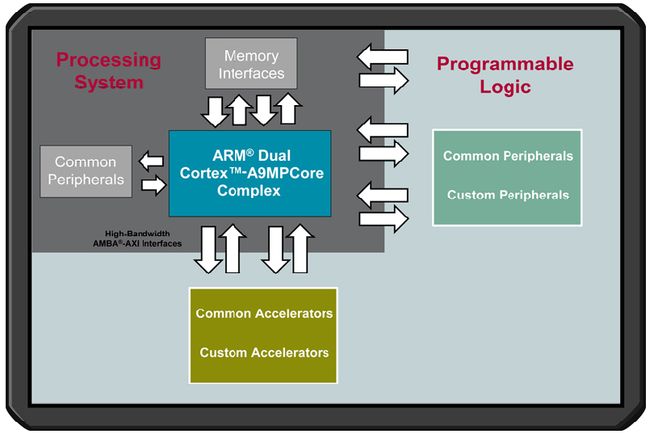
PS: 处理系统(Processing System),与FPGA无关的ARM的SOC的部分。
PL: 可编程逻辑 (Progarmmable Logic),FPGA部分。
APU: 应用处理器单元(Application Processor Unit)。位于PS里面的中心位置。
SCU: Snoop Control Unit,用来保持双核之间的数据Cache的一致性。也就是说,第一个A9 处理器写存储时,只是写在了缓存里,没有进主存,如果第二个A9读操作,涉及到第一个写脏了的数据段,SCU要保证第二个A9的缓存里是最新的数据。如果第二个A9写同样数据段的数据,需要在第一个中体现出写的内容。SCU的存在,才使得两个核成互相联系的 “双核”,才能成为MPsoc。
1、正确规划单板上 FPGA 的定向并将信号分配给特定的引脚,这样可以显著改进系统整体性能、功耗和设计周期。可视化 FPGA 器件与印刷电路板 (PCB) 之间的物理和逻辑互动方式,使您可以优化通过器件的数据流。未正确规划 I/O 配置则可能导致系统性能下降和设计收敛时间延长。单板上 FPGA 器件的布局与其它组件的互动会对 I/O 规划产生巨大影响。
2、首先应确定 FPGA 器件在 PCB 上的定向。还要考虑固定 PCB 组件的位置,以及内部 FPGA 资源。例如,使 FPGA 封装的 GT 接口尽量靠近在 PCB 上与其连接的组件,这样可以缩短 PCB 走线长度,同时减少 PCB 过孔数量。
3、赛灵思建议您设计时首先选择时钟资源,然后再选择管脚。您的时钟选择不仅可以确定特定的管脚,而且还可以支配逻辑布局。正确的时钟选择可以产生非常好的效果。
4、赛灵思 7 系列器件包含 32 个全局时钟缓冲器 (BUFG)。其中 16 个全局时钟缓冲器位于 FPGA 器件水平方向中心的上半部分,而另外 16 个则位于水平方向中心的下半部分。芯片上半部的 PLL 和 MMCM只能连接到水平方向中心以上的 16 个 BUFG 上。而芯片下半部的PLL 和 MMCM 只能连接到水平方向中心以下的 16 个 BUFG 上。选择 PLL 或 MMCM 时,请尽量使用 PLL,因为其具有更严格的抖动控制。在如下情况下也可以使用 MMCM :(1) PLL 已用尽 ; (2)MMCM 可提供所需的高级功能,但 PLL 则不能。
BUFG 组件可以满足设计的大多数时钟要求,但对以下要求不高 :
• 时钟数量
• 设计性能
BUFG 组件易于通过综合调用,并且限制较少,支持大多数普通时钟。
5、使用存储器接口生成器 (MIG) 生成管脚。
千兆位收发器 (GT) 具有特定的管脚要求。假如 GT 采用相同或邻近的 quads,则您可以在多个 GT之间共享参考时钟。赛灵思建议您使用 GT 向导生成内核。有关管脚建议,敬请参阅产品指南。
HP(高性能)和 HR(大范围)Bank在收发信号的速度上存在差异。根据所需的 I/O 速度,在 HP或 HR Bank 间做出选择。
6、从加电到断电,FPGA 器件要经过多个电源阶段,并伴有不同的功率需求 :
• 加电功率
加电功率是 FPGA 器件首次加电时发生的瞬时峰值电流。电压不同时,该电流强度也会发生变化且电流强度取决于 FPGA 器件的结构、电源上升到额定电压的能力,以及器件的工作条件(比如温度以及不同电源之间的排序)。在新型 FPGA 器件架构中,不用担心峰值电流的问题,因为它遵循了适用的上电顺序指南。
• 配置功率
配置功率是指在器件配置期间所需的功率。配置功率通常低于有效功率,因此,除非您的使用过程功耗极低,否则该瞬态不会影响供电需求
• 待机功率
待机功率(又称“设计静态功率”)是器件按设计配置后未对其施加任何外部活动或者未产生任何内部活动时提供的功率。待机功率是设计运行时电源应提供的最小连续功率。
• 有功功率
有功功率(又称“设计动态功率”)是器件运行应用程序时所需功率。有功功率包括待机功率(全部静态功率)以及因设计活动(设计动态功率)产生的功率。有功功率是瞬时发生的,且根据输入数据模式以及设计内部活动的不同每个时钟周期变化一次。
7、配置指的是将特定应用数据加载到 FPGA 器件的内部存储器的过程。
赛灵思 FPGA 配置数据储存在 CMOS 配置锁存(CCL)中,因此配置数据很不稳定,且在每次FPGA 器件断电后都必须重新加载。赛灵思 FPGA 器件可通过来自外部非易失性存储器件的配置引脚自行加载配置数据。而且还可以用外部智能源配置器件。赛灵思 FPGA 配置模式接口涵盖从带有2 引脚的基础串行模式接口到带有50 引脚的高性能主 BPI(同步)模式接口。
8、DMA moves data from a source to a destination location. Memory is often used asdata buffers to match the differences in rate of data source, processing, or data sink, therefore ensuring that the processing stage can achieve maximum throughput.
Off-chip data buffer location can be implemented using off-chip memory attached to customizableMIO orEMIO pins. The memory characteristics affect the performance of moving large buffers, such as file systems onSD cardsor network-attached storage over the GigE controller.
For on-chip buffering, the OCM(片上存储), L2 cache, and DDR controller are the three main sources of sharable buffer space within the PS. The L2 cache and DDR controller provide excellent buffer-access latency for sharing data between the processor and ACP(加速器链接接口) port. Only the ACP can access the L2 cache from PL.
For high-bandwidth accesses to DDR, the HP ports are better suited than ACP. The OCM can be used by software applications as a 256 KB scratchpad accessible by all masters in the PL. A benefit to using OCM is its excellent random-access latency, whereas the L2 cache and DDR memory benefit from memory-access locality.
9、System Monitoring
A rich tool ecosystem exists for monitoring the ARM processors. In a Zynq device, full system-level performance monitoring also uses blocks available in the PS and PL. These are:SCU Global Timer (PS). ARM Performance Monitoring Units (PS). L2 Cache Event Counters (PS). GigE Controller (PS). AXI Performance Monitor (PL). AXI Timer (PL). AXI Traffic Generator (PL).
There are different ways of exercising or acquiring monitoring data from the various blocks. Most peripherals come with an example application packaged with the corresponding bare-metal driver shipped with Xilinx SDK.A list of available Linux drivers is provided in the Xilinx Linux Drivers wiki page.
10、The PS and PL power supplies are independent; however, the PS power supply must be present when the PL power supply is active. The PL can be powered off in applications that do not require the PL.

• PS Power Management
This section describes the design considerations needed to optimize power consumption of a Zynq-7000 AP SoC PS. This includes power management of the APU unit, PS peripherals, clocks and PLLs, caches, SCU, and OCM. Physical Memory(such as DDR2, DDR3, and LPDDR2). I/O(such as MIOs and DDR IOs) It is assumed that the designer understands the impact of power management trade-offs on the overall system.
• PL Power Management
The PL can be powered off in applications that do not require the PL. To do this, independently-connected power supplies are needed for the PS and PL. The PL supplies that can be powered off include VCCINT, VCCAUX, VCCBRAM, and VCCO. Refer to the appropriate data sheet to determine the correct power sequencing.
11、External Clocks
• PS_CLK
On the PS side, a fixed-frequency oscillator in the range of 30-60 MHz is typically used to provide the processor clock PS_CLK. The clock must be a single-ended LVCMOS signal, using the same voltage level as the I/O voltage for MIO bank 0. From this clock, all other PS internal clocks are generated based on three PLLs:ARM, DRM, and IO PLL.
The default PS_CLK frequency used on Xilinx evaluation boards is 33.3 MHz. Other clock frequencies can be used, but the following items are dependent on the PS clock frequency and must be adjusted accordingly:
• The LogiCORE IP Processing System 7 configuration wizard calculates the derived clock dividers and multipliers of each of the PLLs as well as the I/O peripheral clocks such as SPI or UART based on the selected PS_CLK frequency. These values are later used by the first stage boot loader (FSBL) during initialization of the PS.
• The U-Boot board configuration include file.
• The Linux design-specific device tree.
• PL_CLK
On the PL side, single-ended or differential fixed-frequency oscillators can be used as additional clock sources for greater flexibility.
12、PS-Internal Clocks
The CPU clock domain is composed of four separate clocks: CPU_6x4x, CPU_3x2x, CPU_2x, and CPU_1x. These four clocks are named according to their frequencies, which are related by one of two ratios: 6:3:2:1 or 4:2:2:1 (abbreviated 6:2:1 and 4:2:1, respectively). All of the CPU clocks are synchronous to each other. There are two independent DDR clock domains: DDR_3x and DDR_2x. These clocks are asynchronous to each other and the CPU clocks. Most I/O peripherals clocks have dedicated dividers. Each peripheral clock is completely asynchronous to all other clocks.
13、PS - PL Interface
PL AXI channels (AXI_HP, AXI_ACP, and AXI_GP) have asynchronous interfaces between the PS and the PL. The synchronization, where the clock domain crossing occurs, is located inside the PS. Therefore, the PL provides the interface clock to the PS. Each of the aforementioned interfaces could use unique clocks in the PL.
The PS provides four frequency-programmable fabric clocks (FCLK [3:0]) to the PL that are physically spread out along the PS-PL boundary. The clocks can be controlled individually by setting the clock's source (ARM, DDR, or I/O PLL) and the clock's output frequency. There is no guaranteed phase relationship between any of the four FCLK clocks, even when sharing the same clock source. Make sure to use appropriate design constraints when interfacing between multiple FCLK regions. The FCLK clocks are disabled until the PS - PL level shifters are enabled.
14、PL-Internal Clocks
The PL provides clock primitives that are commonly found on FPGA devices, such as global or regional clock buffers (BUFG, BUFR), phased-locked loops (PLL), or mixed-mode clock managers (MMCM). For convenience, the clocking wizard IP core implements a wrapper around the MMCM/PLL primitives with up to eight configurable output clocks. The user can optionally enable dynamic reconfiguration of clock frequencies using the dynamic reconfiguration port (DRP) or an AXI-Lite interface.
TIP: In the simplest case, a complete Zynq-7000 system can be built with a single input clock based on PS_CLK, and all PL clocks are generated from the provided FCLKs and FPGA clocking resources.
15、Reset
• PS Power-On Reset
The PS power-on reset (PS_POR_B) is an active-low signal used to hold the PS in reset until all PS power supplies are stable and at their required voltage levels. This signal should be generated from the power supply power-good signal or from a voltage supervisor chip. At the time PS_POR_B is released, the system clock (PS_CLK) must have been stable for 2,000 clock cycles. PS_POR_B should be pulled high to VCCO_MIO0. When asserting PS_POR_B, the pulse length must be longer than 100 μs.
The power-on reset is the chip master reset. It resets every register in the device that can be reset, resetsall PS RAM (including OCM, Fifos, buffers, etc.) and starts BootROM execution,clearing the PL configuration. When PS_POR_B is held low, all PS I/Os are held in 3-state.
• PS System Reset
The PS system reset (PS_SRST_B) is an active-low signal that is used primarily for debugging proposes. PS_SRST_B must be high to begin the boot process. If PS_SRST_B is not used it can be pulled high to VCCO_MIO1. When asserting PS_SRST_B, the pulse length must be longer than 1 μs.
A PS system reset (PS_SRST_B) resets all functional logic without affecting the debug environment. This differs from a power-on reset (PS_POR_B), which erases the debug configuration. The PS_SRST_B erases all PS RAM, starts BootROM execution, and clears the PL configuration. It does not re-sample the boot-mode strapping pins, unlike the PS_POR_B. The boot mode remains the same as the previous power-on reset, and the security level of the previous boot is retained.
• System Software Reset
The System Software Reset, also called SLCR Soft Reset, is asserted by writing to PSS_RST_CTRL[SOFT_RST] and has the same effect as asserting the PS_SRTS_B pin.All of the PS RAMs are cleared and the PL is reset as well.
• CPU Resets
There are two CPU Resets, one for each ARM core asserted by writing to A9_CPU_RST_CTRL[A9_RSTx]. A CPU Reset to a single processor must be applied from the other CPU, through JTAG or the PL.
• PL Resets
The PS provides four programmable reset signals to the PL (FCLK_RESET [3:0]). The resets are individually programmable and independent of the PL clocks. After a POR or system-wide reset, the reset signals are not de-asserted until the BootROM execution finishes and the PS to PL level shifters are enabled.
16、Using OCM for Handlers
Fetching an interrupt handler from DDR memory might take more time than desired. The Zynq-7000 AP SoC has a large L2 cache, but an interrupt handler may not be cached when an interrupt occurs. In this case, it may be beneficial to place interrupt handlers in on-chip memory (OCM). When this is done, the variability in time spent fetching an interrupt handler is limited to L1 caches misses, leading to reduced jitter.
17、PS Software Boot
Power-On BootROM CRC Check
After power-on, the BootROM is the first software component that executes. An optional 128KB CRC check can be done on the BootROM prior to loading the FSBL. The CRC check is controlled by eFuse settings.
During BootROM execution, the boot header is read from the external storage boot device (SDIO, QSPI flash, NAND flash, or NOR flash) as configured by the mode pins. The header contains information indicating whether the device will boot securely or non-securely.
Secure BOOT Image
The programmable components of a monolithic boot image(BOOT.bin) include:
• PS image components
° An initialization header that can optionally write values to registers. For example the initialization header can be used to increase the CPU clock speed or boot device speed before the BootROM copies and executes the FSBL.
° FSBL.
° Optional secondary-boot loader, such as U-Boot or bare-metal software.
° Optional data images and multiple ELF.
° Optional Linux uImage.
• PL bitstream
The boot image can be made secure, if desired. The PS images and PL bitstreams in a secure boot image are authenticated using a hash-based message authentication code (HMAC) and encrypted using the advanced encryption standard (AES).
A Zynq-7000 AP SoC PL contains AES decryption and HMAC authentication engines. Therefore, the PL must be powered on during the secure boot process, even if the secure boot image does not have a PL bitstream. The BootROM checks whether the PL is powered on prior to reading encrypted images from boot devices, so the embedded system must ensure the PL is powered on before decryption. Because the PL is powered by a different power rail, the embedded system must be designed to ensure the rail has appropriate connectivity to the power regulator.
Bootgen
The programmable components of BOOT.bin are assembled using a Xilinx software tool called Bootgen. Bootgen also encrypts the programmable components when the secure boot option is selected.
18、Profiling and Partitioning
Profiling tools help you determine how to partition an application’s functions between hardware and software for optimal performance. Boot Time、Processor Loading、System Latency、Interrupt Latency.
19、Typical Boot Flow

The boot sequence in a Zynq-7000 AP SoC involves reading the first-stage boot loader (FSBL) from external static storage, typically NAND or NOR flash memory. The BootROM contains the code that is executed after power on reset, and that code reads the FSBL from the external static storage.
After the PS_POR_B pin is de-asserted, hardware samples the boot-strap pins and configures the PS and the PLLs. Software in the PS internal BootROM executes, beginning with code that configures the ARM core and peripherals necessary to copy the FSBL image from the chosen boot device to OCM, and then the code switches execution from the OCM. You can copy the FSBL from the primary boot device mentioned above or you can load it through JTAG. Optionally, in non-secure boot mode, you can execute the FSBL from Quad-SPI/NOR flash that supports execute-in-place.
20、Memory Map
Zynq-7000 All Programmable SoCs support a 4 GB address space.

21、Ordering Information

22、Boot Deivce

You can also implement secondary boot using PCIe, Ethernet, USB, UART, or a custom FPGA interface. You can select an option appropriate to your application.
23、File System
The flash choice influences the file system that can be implemented. The file system choices described below are specific to Linux, but provide a good outline of the issues to be considered.
eMMC and SD cards have a built-in controller that runs the Flash Translation Layer (FTL) firmware, allowing the device to appear to the OS as a block device. Conventional file systems, such FAT or ext3, work with block devices and can be implemented using these devices.
A raw flash device (such as NAND, QSPI, or parallel NOR) requires software management so that reads-from and writes-to memory cells function properly. Linux uses thememory technology device (MTD) subsystem to provide an abstraction layer between the hardware-specific device drivers and higher-level applications. Linux supports file systems that are layered on top of MTD devices, such asJFFS2 andUBIFS. These file systems are designed to include software management algorithms to handle issues like wear leveling and bad block management, and must be used for the device to function properly.
24、DDR Interfaces
The DDR multi-protocol memory controller in the Zynq-7000 AP SoC supports 1.8V DDR2, 1.2V LPDDR2, 1.5V DDR3, and 1.35V DDR3L. It can be configured to provide a 16-bit or 32-bit wide data bus. A 1 GB address map is allocated to the DDR.
The DDR memory controller contains three major blocks: an AXI memory port interface (DDRI), a core controller with a transaction scheduler (DDRC), and a controller with digital PHY (DDRP).
The controller includes a digital PHY with a dedicated set of I/Os. On the fastest speed grade for some Zynq-7000 AP SoC devices, the maximum supported bus clock is 666 2/3 MHzin DDR3 mode. The maximum supported bus clock is 533 MHz in DDR3 mode for all other speed grades. The theoretical maximum bus bit-rate is:
Data transfer rate = 666 2/3 MHz * 2 bits (for double data rate) = 1333 Mb/s per data IO
Using the maximum bus width of 32 bits, the maximum bus bandwidth is 42.6 Gb/s, or 5.3 GB/s.
To facilitate high-bandwidth operation, the DDR interface timing must be properly initialized and calibrated. DDRP includes a DRAM training feature to help automatically determine the timing delays required to align data to the optimal window for reliable data capture. This feature is described in the “Initialization and Calibration” subsection of the “DDR Memory Controller” chapter.
The Zynq-7000 AP SoC tool flow helps automate the DDR bring-up. To do this, the PS DDRC board parameters need to be configured in accordance with Xilinx Answer Record 46778 [Ref 65]. This will import the delay characteristics of DDR signals on the board during the hardware design process. Those characteristics are used to determine the initial values used by the automatic training algorithm, or for calculating static interface timing when the automatic algorithm is not supported by the particular DDR standard. The timing values are part of the design's hardware platform specification and are exported to the SDK and used in PS initialization code that is called by the FSBL.DDR is not used by the BootROM.
25、NAND Memory Controller
The NAND flash controller can support up to 1GB of external NAND flash with either an 8-bit or 16-bit I/O bus for address/data/command. It supports the Open NAND flash Interface 1.0 specification.
Xilinx supported NAND devices range in size from 128MB to 1GB, in both x8 and x16 configurations. Xilinx officially supports NAND devices from Micron and Spansion.
Even in a high-capacity NAND device, the Zynq-7000 AP SoC BootROM will look for a boot image to start in the first 128MB. Therefore, the start of both standard and fallback boot images (if used) must begin in the first 128MB.
Communication with the NAND flash is based on a set of AC timing parameters that vary from device to device. For a Zynq-7000 AP SoC to communicate with a NAND device using the correct timing, a designer should input the relevant timing parameters into the CS0 column on the SMC(Static Memory Controller ) Timing Calculation page based on the device's AC timing values.
The CS0 cycle is automatically calculated based on the NAND clock frequency. The values are exported to the SDK's PS initialization code as part of the design's Hardware Platform Specification. The initialization code writes those values to the smc.SET_CYCLE register.
BootROM reads from NAND flash prior to executing PS initialization code, using a set of initial values stored in the smc.SET_CYCLE register. Further details on those values can be found in the NAND Boot subsection of the “Boot and Configuration” chapter.
In NAND flash, reads and writes occur in pages, while erasures occur in blocks. Because NAND flash does not behave like random access memory, Linux systems use it as a memory technology device (MTD) that provides an abstraction layer, allowing software to access the device using the MTD subsystem API. That API is common among different flash types and technologies. MTD is not a block device and it lacks the software management algorithms to handle issues like wear leveling and bad block management. Instead of traditional file systems like ext2, ext3, and FAT (which work on top of block devices), the file system must be designed to work on top of raw flash, such as JFFS2 or UBIFS. JFFS2 works on top of MTD subsystems. UBIFS works on top of UBI subsystems, and those work on top of MTD subsystems to provide software management algorithms required for NAND devices.
26、Xilinx tools auto generate the ps7_init.tcl and ps7_init.c files when Vivado exports a design. The ps7_init.c file is an initialization file auto generated by Vivado and used by the first stage boot loader (FSBL) to initialize the PS.
The Xilinx SDK has a memory test that can verify the DDR memory and the signal integrity of the memory controller and DDR interface. The bare-metal memory test application can be used to exercise a DDR memory power-on self-test. The DRAM test application template is located in your installation directory at SDK\2014.2\data\embeddedsw\lib\sw_apps\zynq_dram_test.
Example drivers are available for many PS peripherals. They can be found in the SDK\
27、You stitch the FSBL with the bitstream and an application using the Bootgen program. SDK has a Create Boot Image wizard option, to add the partition images and create a bootable image that you can then flash.
The rules are:
•The first partition must be the FSBL ELF followed by the bitstream partition and then the application ELF.
•Bitstream is optional. FSBL does a handoff to the first application in the BIF order.
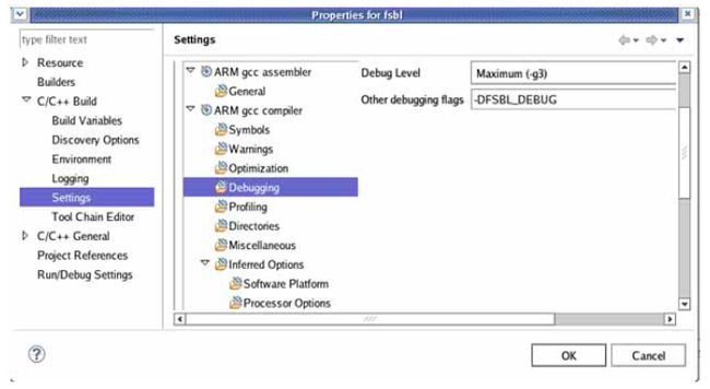
You can set compilation flags using the C/C++ settings in SDK FSBL project, as shown in the following figure.
28、A utility program called Bootgen is provided to create a single boot image file suitable for ROM or flash memory programming. It creates the image by building the required boot header, appending tables that describe the following partitions, and processing the input data files (ELF files, FPGA bitstreams, and other binary files) to partitions. It has features for assigning specific destination memory addresses or imposing alignment requirements for each partition. It also supports the encryption, authentication, or performing checksums on each partition.
The utility is driven by a configuration file known as the Boot Image Format (BIF) file with a file extension of *.bif.
29、Boot Image Format
The boot image format consists of the following:
•BootROM header
•FSBL image
•One or more partition images
•Unused space, if available
