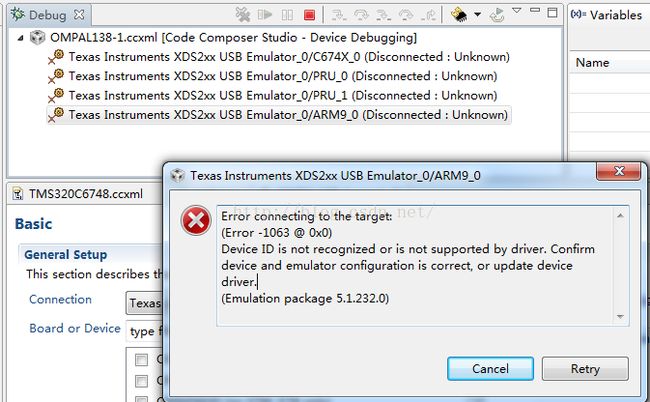
连接OMAPL138 ARM9核时出现的Error connecting to the target: (Error -1063 @ 0x0)问题
这里写代码片C6748的程序可以通过仿真器,仿真在OMAPL138上运行,但是重新上电就没有了,所以我想把C6748程序通过仿真器固化到OMAPL138 NAND flash中,看看实际的效果,但是连接的ARM9核的时候,一直出现连接不上的问题,如下图所示。
仿真器:XDS200 USB
CCS v5.5
Win7 64位
后来更改了下OMAPL138-1.ccxml文件,如下图所示:
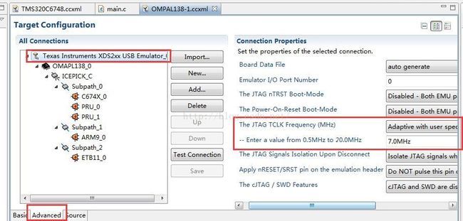
再重新连接,就可以连接上了,可以看到提示正常了。
简单描述下使用仿真器把C6748的固化到OMAPL138的步骤。
1. 将开发板启动模式调好,我这里用的是创龙的,将拨码开关调到00101;
2. 查看仿真器连接是否正常;
3. 新建工程配置文件,VIEW- –Target Configuration,选择对应的仿真器,默认XDS100V2,我这里用的是XDS200,选择好对应的目标器件,OMAPL138.
然后点击左上角的Target Configuration,按下图配置一下,点击SAVE保存。然后测试下仿真器,Test Configuration,测试正常即可。
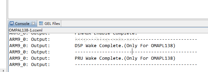
4. 选择工具栏上的RUN—Debug,会看到OMAPL138-1.ccxml下面出现四个子项,如上面第一张图所示,选择最后一个ARM9那个,右键,选择OPEN GEL VIEW,然后加载omapl138.gel文件,成功后,右键ARM9选项,选择连接,看到上面第三个图的输出时,即可看到连接成功。
5. 连接ARM9核成功后,连接第一个DPS C6748选项,右键 connect target ,会看到下图所示;

6.然后点击ARM9第四个选项,选择工具栏中的”Run->Load->Load Program”,选择nand-writer.out文件,点击OK。接着点击启动按键,会看到下面的文字:
[ARM9_0] Starting DA8xx_NANDWriter.
DA8XX/OMAP-L1XX part detected. Its an ARM boot device
You require two images to boot this device
1) ARM UBL in AIS file format.
2) U-Boot image in raw binary format
To generate the AIS format file, you need to run the ARM/DSP .out (COFF) file generated from CCS build through the AISGen tool.
Enter the image type (one of “armais” “uboot” “other”)
这里提示让输入image的类型,这里选择输入“armais”,不带双引号,然后回车,可以看到下面的文字:
Enter the image type (one of “armais” “uboot” “other”)
armais
Enter the file Name
然后会提示 “Enter the file Name”,这时输入armdsp.bin的路径,再按回车键,会看到下面文字提示:
Enter the image type (one of “armais” “uboot” “other”)
armais
Enter the file Name
F:\1tronlong\omapl138\armdsp.bin
Number of blocks needed for data: 0x1
Attempting to start write in block number 0x1.
Unprotecting blocks 0x1 through 0x1.
Erasing block 0x1 through 0x1.
Writing image data to Block 0x1, Page 0x0
Writing image data to Block 0x1, Page 0x1
Writing image data to Block 0x1, Page 0x2
Writing image data to Block 0x1, Page 0x3
Writing image data to Block 0x1, Page 0x4
Writing image data to Block 0x1, Page 0x5
Writing image data to Block 0x1, Page 0x6
Protecting the entire NAND flash.
NAND boot preparation was successful!
说明烧写成功。
7. 烧写完 armdsp.bin 镜像后, 拔下开发板仿真器,将开发板的拨码关 1~5 号对应拨到 01110 档位 ,这是 NAND FLASH 启动档位。 启动开发板即可 看到 底板 LED流水灯效果。