Active Low-Pass Filter Design 低通滤波器设计
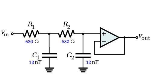
2nd order RC Low-pass Filter
Center frequency fc = 23405.13869[Hz]
Q factor Q = 0.333333333333
Sallen–Key topology
http://en.wikipedia.org/wiki/Sallen%E2%80%93Key_topology

A low-pass filter, which is implemented with a Sallen–Key topology, with fc=15.9 kHz and Q = 0.5
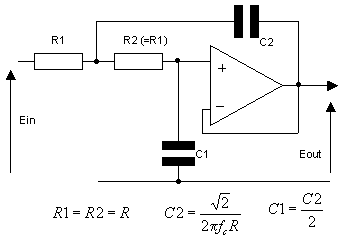
这个电路是一个单位增益的电路,改变Sallen-Key 滤波器的增益同时就改变了滤波器的幅频特性和类型。
实际上Sallen-Key 滤波器就是增益为1的Butterworth 滤波器。
Sallen & Key 2nd order low pass filter -
- Non-inverting
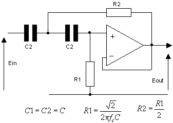
Sallen & Key 2nd order high pass filter - Non-inverting
Sallen-Key Low-pass Filter
http://sim.okawa-denshi.jp/en/OPseikiLowkeisan.htm
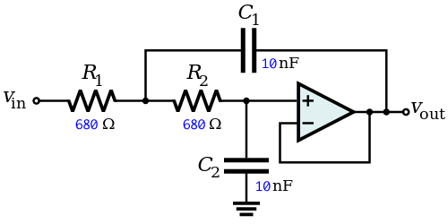
Cut-off frequency fc = 23405.13869[Hz]
Quality factor Q = 0.5
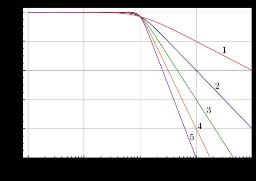
Butterworth Low-pass Filter
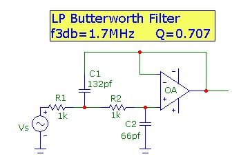
Transfer function
http://mathscinotes.wordpress.com/2011/06/10/filter-design-details/
Figure 4 shows the Sallen-Key circuit, which is a very commonly used circuit for this type of application
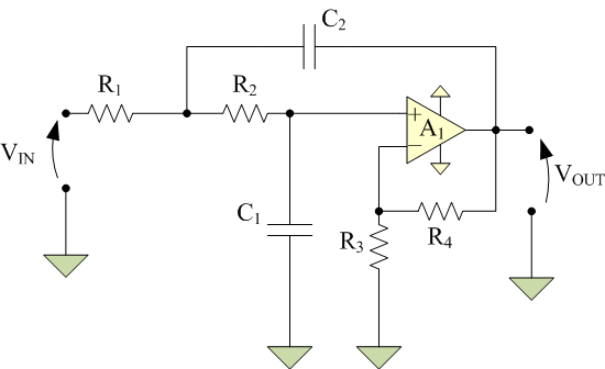 .
.
Analysis of Sallen-Key Circuit
Figure 5 shows a standard Kirchoff’s Voltage Law (KVL) analysis of the Sallen-Key circuit.
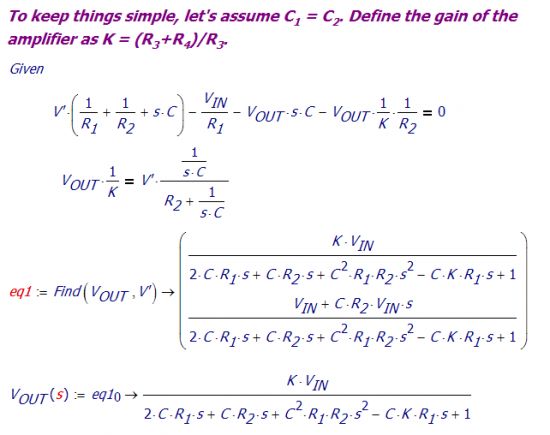
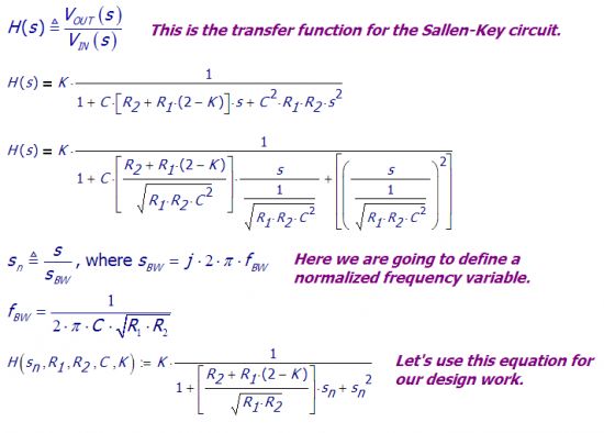
I usually do not work with filter equations in the form shown in Figure 5.
I like to normalize the frequency variable, s, relative to the filter bandwidth

Normalized Form
Figure 6 shows the Butterworth equation normalized to the filter bandwidth.
This is the equation form normally shown in the filter design tables.
Component Determination
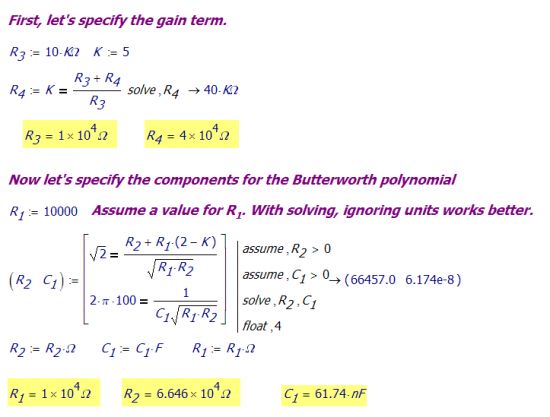
Figure 7 shows how we can determine the component values required for this implementation
using the equation solving abilities of Mathcad.
We can now generate a plot of the filter magnitude characteristic using these component values
Gain Characteristic
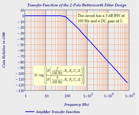
Figure 8 shows the gain characteristic of this design.
As expected, we are seeing 120 dB of ripple attenuation.
The gain at 0 Hz is 5, so that requirement is also met.
Conclusion
This was a good example of a common filter design problem.
I have used both circuit simulators and computer algebra software to design these filters.
I have come to like computer algebra software for this kind of work because it gives me equations.
These equations allow me to see how the output varies as a function of individual component values.
This means that I can see useful approximations.
Multiple feedback topology
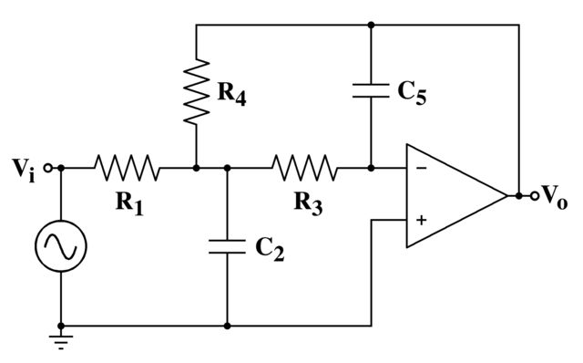
Multiple feedback topology is an electronic filter topology which is used to implement an electronic filter by adding two poles to the transfer function.
A diagram of the circuit topology for a second order low pass filter is shown in the figure on the right.
Analog filters and specifications swimming: Input bias current makes a difference
When designing an analog active filter, you may be overwhelmed with the list of factors to consider.
But, as you start to select your amplifier(s), I suggest that you start with the simple things: input bias current.
Yes, you also need to pay attention to amplifier bandwidth, slew rate, noise, common-mode voltage range (sometimes),
and offset voltage, but dealing with the input bias current has to be the easiest.
First of all, you need to know something about the circuit configurations that you will be using.
The most common configurations in use today are the Sallen-Key and multiple-feedback (MFB) topologies.
These topologies are used in lowpass, highpass, bandpass, and bandstop (notch) filters.
Let’s take a look at second-order, lowpass filters (Figure 1).
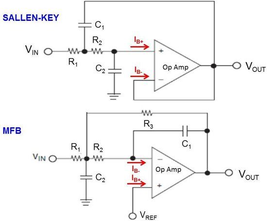
Figure 1. Second-order lowpass filters
Notice the resistors that connect directly to the inverting and/or non-inverting terminals.
This is the place where the input bias (IB+and IB-) current flows to create a voltage that looks like the amplifier’s offset voltage.
So, what value of resistors might you expect and what is the allowable amplifier input bias current?
The magnitude of the input bias current primarily depends on the amplifier’s silicon technology.
Figure 2 shows some typical input stages for CMOS and bipolar amplifiers.
The amount of current flowing in or out of the IB+ and IB- terminals depends on the amplifier technology and circuit design,
so it is hard to give an exact answer. However, you can make some general statements.
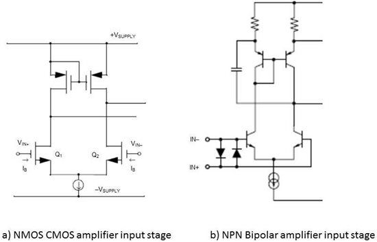
Figure 2. Typical differential input stages for CMOS (a) and bipolar (b) amplifiers
CMOS amplifiers typically generate input bias currents in a range of up to 400 pA.
If you find units of nanoamps up to several milliamps, that’s probably a bipolar amplifier.
More information about the input bias currents of amplifiers is available in my earlier blog,
“How to read a precision op amp data sheet.”
Now, how big are the lowpass filter resistors in Figure 1?
Resistor values depend on the capacitor’s magnitude.
So, let’s first talk about the capacitors.
When designing a filter, whether it uses a lowpass, highpass, bandpass, or bandstop topology,
the capacitor technology should be C0G or NPO.
There are a lot of different types of capacitors such as X7R, Z5U, and Y5V.
But the C0G and NPO capacitors are set apart from the others because they have a low-voltage and low-frequency coefficients.
If these coefficients are not low, the capacitance values change as signals travel through the filter.
When the capacitors change, the filter response also changes.
I will go into more details about these capacitor characteristics next time,
but this fact limits the acceptable range for your filter capacitors.
C0G capacitor values range up to 100 nF.
Given this range, the approximate upper range of the resistors is 30 kOhms from my survey of
Gaussian to 6 dB, linear phase 0.05°,
Butterworth, 0.2 dB Chebyshev, linear phase 0.5°,
Bessel and Gaussian to 12 dB filters.
Now we have something to work with!
In Figure 1a, the voltage error caused by the resistors and IB+ is VOS-IB = (R1 + R2)*IB+.
To get the total offset error of this system you add VOS-IB to the amplifier’s offset voltage (VOS).
If you want the input offset error to be equal to or below 1.22 mV (12-bit LSB in a 5 V system),
then the maximum allowable input bias current for the Figure 1a circuits is 10 nA, with VOS-MAX = 200 uV.
This translates into using CMOS op amps or bipolar op amps with sufficiently low IB and low VOS.
You want to do a little research?
Look into these questions and find your answers by using the Texas Instruments
WEBENCH®Filter Designer program.
http://www.ti.com/tool/filterpro
