【牛客网刷题】VL11-VL24 组合逻辑 & 时序逻辑
目录
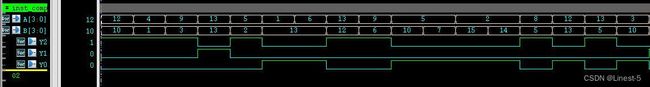
VL11 4位数值比较器电路
VL12 4bit超前进位加法器电路
VL13 优先编码器电路①
VL14 用优先编码器①实现键盘编码电路
VL15 优先编码器Ⅰ
VL16 使用8线-3线优先编码器Ⅰ实现16线-4线优先编码器
VL17 用3-8译码器实现全减器
VL18 实现3-8译码器
VL19 使用3-8译码器①实现逻辑函数
VL20 数据选择器实现逻辑电路
VL21 根据状态转移表实现时序电路
VL22 根据状态转移图实现时序电路
VL23 ROM的简单实现
VL24 边沿检测
VL11 4位数值比较器电路
题目描述
某4位数值比较器的功能表如下。
请用Verilog语言采用门级描述方式,实现此4位数值比较器
| input |
output |
|||||
| A[3]B[3] |
A[2]B[2] |
A[1]B[1] |
A[0]B[0] |
Y2(A>B) |
Y1(A=B) |
Y0(A |
| A[3]>B[3] |
x |
x |
x |
1 |
0 |
0 |
| A[3] |
x |
x |
x |
0 |
0 |
1 |
| A[3]=B[3] |
A[2]>B[2] |
x |
x |
1 |
0 |
0 |
| A[3]=B[3] |
A[2] |
x |
x |
0 |
0 |
1 |
| A[3]=B[3] |
A[2]=B[2] |
A[1]>B[1] |
x |
1 |
0 |
0 |
| A[3]=B[3] |
A[2]=B[2] |
A[1] |
x |
0 |
0 |
1 |
| A[3]=B[3] |
A[2]=B[2] |
A[1]=B[1] |
A[0]>B[0] |
1 |
0 |
0 |
| A[3]=B[3] |
A[2]=B[2] |
A[1]=B[1] |
A[0] |
0 |
0 |
1 |
| A[3]=B[3] |
A[2]=B[2] |
A[1]=B[1] |
A[0]=B[0] |
0 |
1 |
0 |
RTL 设计
`timescale 1ns/1ns

module comparator_4(
	input		[3:0]       A   	,
	input	    [3:0]		B   	,

 	output	 wire		    Y2    , //A>B
	output   wire           Y1    , //A=B
    output   wire           Y0      //A B[3]) | ((A[3] == B[3]) & (A[2] > B[2])) | ((A[3] == B[3]) & (A[2] == B[2]) & (A[1] > B[1])) | ((A[3] == B[3]) & (A[2] == B[2]) & (A[1] == B[1]) & (A[0] > B[0]));
assign Y1 = (A[3] == B[3]) & (A[2] == B[2]) & (A[1] == B[1]) & (A[0] == B[0]);
assign Y0 = (~Y1) & (~Y2);

endmodule
testbench 设计
`timescale 1ns/1ns

module tb_comparator_4();

reg  [3:0]    A;
reg  [3:0]    B;
wire          Y2;
wire          Y1;
wire          Y0;

initial begin
	A <= 4'd12;
	B <= 4'd10;
	#200
	$finish;
end

always #10 A <= {$random} % 5'd16;
always #10 B <= {$random} % 5'd16;

comparator_4 inst_comparator_4 (
	.A(A),
	.B(B),
	.Y2(Y2),
	.Y1(Y1),
	.Y0(Y0)
);

//verdi
initial begin
	$fsdbDumpfile("tb_comparator_4.fsdb");
	$fsdbDumpvars(0);
end

endmodule
仿真测试
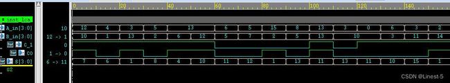
VL12 4bit超前进位加法器电路
题目描述
4bit超前进位加法器的逻辑表达式如下:
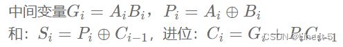
请用Verilog语言采用门级描述方式,实现此4bit超前进位加法器,接口电路如下:

输入描述
A_in [3:0]
B_in [3:0]
C_1
类型:wire
输出描述
S [3:0]
CO
类型:wire
RTL 设计
`timescale 1ns/1ns

module lca_4(
	input		 [3:0]      A_in  ,
	input	     [3:0]		B_in  ,
    input                   C_1   ,

 	output	wire			CO    ,
	output  wire [3:0]	    S
);

wire  [3:0]    G;
wire  [3:0]    P;
wire  [3:0]    C;

//第0位
assign G[0] = A_in[0] & B_in[0];
assign P[0] = A_in[0] ^ B_in[0];
assign C[0] = G[0] | (P[0] & C_1);
assign S[0] = P[0] ^ C_1;

//第1位
assign G[1] = A_in[1] & B_in[1];
assign P[1] = A_in[1] ^ B_in[1];
assign C[1] = G[1] | (P[1] & C[0]);
assign S[1] = P[1] ^ C[0];

//第2位
assign G[2] = A_in[2] & B_in[2];
assign P[2] = A_in[2] ^ B_in[2];
assign C[2] = G[2] | (P[2] & C[1]);
assign S[2] = P[2] ^ C[1];

//第3位
assign G[3] = A_in[3] & B_in[3];
assign P[3] = A_in[3] ^ B_in[3];
assign C[3] = G[3] | (P[3] & C[2]);
assign S[3] = P[3] ^ C[2];

assign CO = C[3];

endmodule
testbench 设计
`timescale 1ns/1ns

module tb_lca_4();

reg  [3:0]   A_in;
reg  [3:0]   B_in;
reg          C_1;
wire         CO;
wire         S;

initial begin
	A_in <= 4'd12;
	B_in <= 4'd10;
	C_1  <= 1'd1;
	#200
	$finish;
end

always #10 A_in <= {$random} % 5'd16;
always #10 B_in <= {$random} % 5'd16;
always #10 C_1  <= {$random} % 2'd2;

lca_4 inst_lca_4 (
	.A_in(A_in),
	.B_in(B_in),
	.C_1(C_1),
	.CO(CO),
	.S(S)
);

//verdi
initial begin
	$fsdbDumpfile("tb_lca_4.fsdb");
	$fsdbDumpvars(0);
end

endmodule
仿真测试
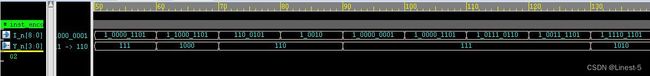
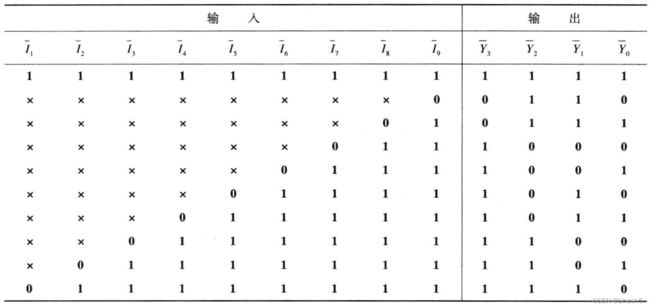
VL13 优先编码器电路①
题目描述
下表是某优先编码器的真值表。
①请用Verilog实现此优先编码器

RTL 设计
`timescale 1ns/1ns

module encoder_0(
   input      [8:0]      I_n,
   output reg [3:0]      Y_n
);

always @(*) begin
	casez(I_n)
		9'b111111111: begin
			Y_n <= 4'b1111;
		end
		9'b0????????: begin
			Y_n <= 4'b0110;
		end
		9'b10???????: begin
			Y_n <= 4'b0111;
		end
		9'b110??????: begin
			Y_n <= 4'b1000;
		end
		9'b1110?????: begin
			Y_n <= 4'b1001;
		end
		9'b11110????: begin
			Y_n <= 4'b1010;
		end
		9'b111110???: begin
			Y_n <= 4'b1011;
		end
		9'b1111110??: begin
			Y_n <= 4'b1100;
		end
		9'b11111110?: begin
			Y_n <= 4'b1101;
		end
		9'b111111110: begin
			Y_n <= 4'b1110;
		end
		default: begin
			Y_n <= 4'bz;
		end
	endcase
end

endmodule
testbench设计
`timescale 1ns/1ns

module tb_encoder_0();

reg  [8:0]   I_n;
wire [3:0]   Y_n;

initial begin
	I_n <= 9'd0;
	#200
	$finsih;
end

always #10 I_n <= {$random} % 10'd512;

encoder_0 inst_encoder_0 (
	.I_n(I_n),
	.Y_n(Y_n)
);

//verdi
initial begin
	$fsdbDumpfile("tb_encoder_0.fsdb");
	$fsdbDumpvars(0);
end

endmodule
仿真测试
VL14 用优先编码器①实现键盘编码电路
题目描述
请使用优先编码器①实现键盘编码电路,可添加并例化题目中已给出的优先编码器代码。
10个按键分别对应十进制数0-9,按键9的优先级别最高;按键悬空时,按键输出高电平,按键按下时,按键输出低电平;键盘编码电路的输出是8421BCD码。
要求:键盘编码电路要有工作状态标志,以区分没有按键按下和按键0按下两种情况。
优先编码器真值表如下图:
优先编码器代码如下:
module encoder_0(
    input      [8:0]  I_n ,
    output reg [3:0]  Y_n
);
always @(*) begin
    casex(I_n)
        9'b111111111 : Y_n = 4'b1111;
        9'b0xxxxxxxx : Y_n = 4'b0110;
        9'b10xxxxxxx : Y_n =     4'b0111;
        9'b110xxxxxx : Y_n = 4'b1000;
        9'b1110xxxxx : Y_n = 4'b1001;
        9'b11110xxxx : Y_n = 4'b1010;
        9'b111110xxx : Y_n = 4'b1011;
        9'b1111110xx : Y_n = 4'b1100;
        9'b11111110x : Y_n = 4'b1101;
        9'b111111110 : Y_n = 4'b1110;
        default : Y_n = 4'b1111;
    endcase
end

endmodule
RTL设计
`timescale 1ns/1ns

module encoder_0(
   input      [8:0]     I_n,
   output reg [3:0]     Y_n
);

always @(*)begin
   casex(I_n)
      9'b111111111 : Y_n = 4'b1111;
      9'b0xxxxxxxx : Y_n = 4'b0110;
      9'b10xxxxxxx : Y_n = 4'b0111;
      9'b110xxxxxx : Y_n = 4'b1000;
      9'b1110xxxxx : Y_n = 4'b1001;
      9'b11110xxxx : Y_n = 4'b1010;
      9'b111110xxx : Y_n = 4'b1011;
      9'b1111110xx : Y_n = 4'b1100;
      9'b11111110x : Y_n = 4'b1101;
      9'b111111110 : Y_n = 4'b1110;
      default      : Y_n = 4'b1111;
   endcase
end

endmodule

module key_encoder(
      input       [9:0]     S_n,
      output wire [3:0]     L,
      output wire           GS
);

wire [3:0]   L_reg;

encoder_0 inst_encoder_0 (
   .I_n(S_n[9:1]),
   .Y_n(L_reg)
);

assign L = ~L_reg;
assign GS = ~(&S_n);

endmodule
testbench 设计
`timescale 1ns/1ns

module tb_encoder_0();

reg  [9:0]     S_n;
wire [3:0]     L;
wire           GS;

initial begin
	S_n <= 10'b0000_0000_00;
	#20
	S_n <= 10'b1111_1111_11;
	#20
	S_n <= 10'b1111_1111_10;
	#20
	S_n <= 10'b1111_1111_01;
	#20
	S_n <= 10'b1111_1110_11;
	#20
	S_n <= 10'b1111_1101_11;
	#20
	S_n <= 10'b1111_1011_11;
	#20
	S_n <= 10'b1111_0111_11;
	#20
	S_n <= 10'b1110_1111_11;
	#20
	S_n <= 10'b1101_1111_11;
	#20
	S_n <= 10'b1011_1111_11;
	#20
	S_n <= 10'b0111_1111_11;
	#20
	S_n <= 10'b0111_1111_11;
	#50
	$finish;
end

key_encoder inst_key_encoder(
	.S_n (S_n),
	.L   (L),
	.GS  (GS)
	);

initial begin
	$fsdbDumpfile("tb_encoder_0.fsdb");
	$fsdbDumpvars(0);
end

endmodule
仿真测试
VL15 优先编码器Ⅰ
题目描述
下表是8线-3线优先编码器Ⅰ的功能表。
①请根据该功能表,用Verilog实现该优先编码器Ⅰ。
| EI |
I[7] |
I[6] |
I[5] |
I[4] |
I[3] |
I[2] |
I[1] |
I[0] |
Y[2] |
Y[1] |
Y[0] |
GS |
EO |
| 0 |
x |
x |
x |
x |
x |
x |
x |
x |
0 |
0 |
0 |
0 |
0 |
| 1 |
0 |
0 |
0 |
0 |
0 |
0 |
0 |
0 |
0 |
0 |
0 |
0 |
1 |
| 1 |
1 |
x |
x |
x |
x |
x |
x |
x |
1 |
1 |
1 |
1 |
0 |
| 1 |
0 |
1 |
x |
x |
x |
x |
x |
x |
1 |
1 |
0 |
1 |
0 |
| 1 |
0 |
0 |
1 |
x |
x |
x |
x |
x |
1 |
0 |
1 |
1 |
0 |
| 1 |
0 |
0 |
0 |
1 |
x |
x |
x |
x |
1 |
0 |
0 |
1 |
0 |
| 1 |
0 |
0 |
0 |
0 |
1 |
x |
x |
x |
0 |
1 |
1 |
1 |
0 |
| 1 |
0 |
0 |
0 |
0 |
0 |
1 |
x |
x |
0 |
1 |
0 |
1 |
0 |
| 1 |
0 |
0 |
0 |
0 |
0 |
0 |
1 |
x |
0 |
0 |
1 |
1 |
0 |
| 1 |
0 |
0 |
0 |
0 |
0 |
0 |
0 |
1 |
0 |
0 |
0 |
1 |
0 |
RTL设计
module encoder_83(
   input       [7:0]      I   ,
   input                  EI  ,

   output wire [2:0]      Y   ,
   output wire            GS  ,
   output wire            EO
);

reg  [2:0]     Y_reg;

always @(I or EI) begin
	if (!EI) begin
		Y_reg = 3'b000;
	end
	else begin
		casez(I)
			8'b00000000: begin
				Y_reg <= 3'b000;
			end
			8'b1???????: begin
				Y_reg <= 3'b111;
			end
			8'b01??????: begin
				Y_reg <= 3'b110;
			end
			8'b001?????: begin
				Y_reg <= 3'b101;
			end
			8'b0001????: begin
				Y_reg <= 3'b100;
			end
			8'b00001???: begin
				Y_reg <= 3'b011;
			end
			8'b000001??: begin
				Y_reg <= 3'b010;
			end
			8'b0000001?: begin
				Y_reg <= 3'b001;
			end
			8'b00000001: begin
				Y_reg <= 3'b000;
			end
			default: begin
				Y_reg <= 3'b000;
			end
		endcase
	end
end

assign Y  = Y_reg;
assign GS = (EI==1'b0) ? 1'b0 : (((|I) == 1'b0) ? 1'b0 : 1'b1);
assign EO = (EI==1'b0) ? 1'b0 : (~GS);

endmodule
testbench设计
`timescale 1ns/1ns

module tb_encoder_83();

   reg   [7:0]     I;
   reg             EI;
   wire  [2:0]     Y;
   wire            GS;
   wire            EO;

initial begin
	I  <= 8'd0;
	EI <= 1'b0;
	#200
	$finish;
end

always #10 I  <= {$random} % 9'd256;
always #10 EI <= {$random} % 2'd2;

encoder_83 inst_encoder_83 (
	.I   (I),
	.EI  (EI),
	.Y   (Y),
	.GS  (GS),
	.EO  (EO)
);

//fsdb
initial begin
	$fsdbDumpfile("tb_encoder_83.fsdb");
	$fsdbDumpvars(0);
end

endmodule
仿真测试
VL16 使用8线-3线优先编码器Ⅰ实现16线-4线优先编码器
题目描述
②请使用2片该优先编码器Ⅰ及必要的逻辑电路实现16线-4线优先编码器。优先编码器Ⅰ的真值表和代码已给出。
可将优先编码器Ⅰ的代码添加到本题答案中,并例化。
RTL 设计
`timescale 1ns/1ns

module encoder_83(
   input      [7:0]       I   ,
   input                  EI  ,

   output wire [2:0]      Y   ,
   output wire            GS  ,
   output wire            EO
);
assign Y[2] = EI & (I[7] | I[6] | I[5] | I[4]);
assign Y[1] = EI & (I[7] | I[6] | ~I[5]&~I[4]&I[3] | ~I[5]&~I[4]&I[2]);
assign Y[0] = EI & (I[7] | ~I[6]&I[5] | ~I[6]&~I[4]&I[3] | ~I[6]&~I[4]&~I[2]&I[1]);

assign EO = EI&~I[7]&~I[6]&~I[5]&~I[4]&~I[3]&~I[2]&~I[1]&~I[0];

assign GS = EI&(I[7] | I[6] | I[5] | I[4] | I[3] | I[2] | I[1] | I[0]);
//assign GS = EI&(| I);

endmodule

module encoder_164(
   input      [15:0]      A   ,
   input                  EI  ,

   output wire [3:0]      L   ,
   output wire            GS  ,
   output wire            EO
);

wire  [2:0]    Y0;
wire  [2:0]    Y1;
wire           GS0;
wire           GS1;
wire           E0_0;
wire           E0_1;

encoder_83 inst_encoder_83_0 (
	.I(A[7:0]),
	.EI(EI),
	.Y(Y0),
	.GS(GS0),
	.EO(EO_0)
);

encoder_83 inst_encoder_83_1 (
	.I(A[15:8]),
	.EI(EI),
	.Y(Y1),
	.GS(GS1),
	.EO(EO_1)
);

assign L[3] = GS1;
assign L[2] = (L[3]==0) ? Y0[2] : Y1[2];
assign L[1] = (L[3]==0) ? Y0[1] : Y1[1];
assign L[0] = (L[3]==0) ? Y0[0] : Y1[0];

assign GS = GS0 | GS1;

assign EO = EO_0 & EO_1;

endmodule
testbench 设计
`timescale 1ns/1ns

module tb_encoder_164();
reg   [15:0]     A ;
reg              EI;
wire  [3:0]      L ;
wire             GS;
wire             EO;

initial begin
	A  <= 16'd0;
	EI <= 1'b0;
	#200
	$finish;
end

always #10 A  <= {$random} % 17'd65536;
always #10 EI <= {$random} % 2'd2;

encoder_164 encoder_164_inst(
	.A (A ),
	.EI(EI),
	.L (L ),
	.GS(GS),
	.EO(EO)
	);

//fsdb
initial begin
	$fsdbDumpfile("tb_encoder_164.fsdb");
	$fsdbDumpvars(0);
end

endmodule
仿真测试
VL17 用3-8译码器实现全减器
题目描述
请使用3-8译码器和必要的逻辑门实现全减器,全减器接口图如下,A是被减数,B是减数,Ci是来自低位的借位,D是差,Co是向高位的借位。

3-8译码器代码如下,可将参考代码添加并例化到本题答案中。
RTL 设计
module decoder_38(
   input             E      ,
   input             A0     ,
   input             A1     ,
   input             A2     ,

   output reg       Y0n    ,
   output reg       Y1n    ,
   output reg       Y2n    ,
   output reg       Y3n    ,
   output reg       Y4n    ,
   output reg       Y5n    ,
   output reg       Y6n    ,
   output reg       Y7n
);

always @(*)begin
   if(!E)begin
      Y0n = 1'b1;
      Y1n = 1'b1;
      Y2n = 1'b1;
      Y3n = 1'b1;
      Y4n = 1'b1;
      Y5n = 1'b1;
      Y6n = 1'b1;
      Y7n = 1'b1;
   end
   else begin
      case({A2,A1,A0})
         3'b000 : begin
                     Y0n = 1'b0; Y1n = 1'b1; Y2n = 1'b1; Y3n = 1'b1;
                     Y4n = 1'b1; Y5n = 1'b1; Y6n = 1'b1; Y7n = 1'b1;
                  end
         3'b001 : begin
                     Y0n = 1'b1; Y1n = 1'b0; Y2n = 1'b1; Y3n = 1'b1;
                     Y4n = 1'b1; Y5n = 1'b1; Y6n = 1'b1; Y7n = 1'b1;
                  end
         3'b010 : begin
                     Y0n = 1'b1; Y1n = 1'b1; Y2n = 1'b0; Y3n = 1'b1;
                     Y4n = 1'b1; Y5n = 1'b1; Y6n = 1'b1; Y7n = 1'b1;
                  end
         3'b011 : begin
                     Y0n = 1'b1; Y1n = 1'b1; Y2n = 1'b1; Y3n = 1'b0;
                     Y4n = 1'b1; Y5n = 1'b1; Y6n = 1'b1; Y7n = 1'b1;
                  end
         3'b100 : begin
                     Y0n = 1'b1; Y1n = 1'b1; Y2n = 1'b1; Y3n = 1'b1;
                     Y4n = 1'b0; Y5n = 1'b1; Y6n = 1'b1; Y7n = 1'b1;
                  end
         3'b101 : begin
                     Y0n = 1'b1; Y1n = 1'b1; Y2n = 1'b1; Y3n = 1'b1;
                     Y4n = 1'b1; Y5n = 1'b0; Y6n = 1'b1; Y7n = 1'b1;
                  end
         3'b110 : begin
                     Y0n = 1'b1; Y1n = 1'b1; Y2n = 1'b1; Y3n = 1'b1;
                     Y4n = 1'b1; Y5n = 1'b1; Y6n = 1'b0; Y7n = 1'b1;
                  end
         3'b111 : begin
                     Y0n = 1'b1; Y1n = 1'b1; Y2n = 1'b1; Y3n = 1'b1;
                     Y4n = 1'b1; Y5n = 1'b1; Y6n = 1'b1; Y7n = 1'b0;
                  end
         default: begin
                     Y0n = 1'b1; Y1n = 1'b1; Y2n = 1'b1; Y3n = 1'b1;
                     Y4n = 1'b1; Y5n = 1'b1; Y6n = 1'b1; Y7n = 1'b1;
                  end
      endcase
   end
end

endmodule

module decoder1(
   input             A     ,
   input             B     ,
   input             Ci    ,

   output wire       D     ,
   output wire       Co
);

wire   Y0,Y1,Y2,Y3,Y4,Y5,Y6,Y7;

decoder_38 inst(1'b1,Ci,B,A,Y0,Y1,Y2,Y3,Y4,Y5,Y6,Y7);

assign D  = ~(Y1 & Y2 & Y4 & Y7);
assign Co = ~(Y1 & Y2 & Y3 & Y7);

endmodule
testbench 设计
`timescale 1ns/1ns

module tb_decoder_38();
	reg        A;
	reg        B;
	reg        Ci;
	wire       D;
	wire       Co;

initial begin
	A  <= 1'd0;
	B  <= 1'd0;
	Ci <= 1'd0;
	#200
	$finish;
end

always #10 A  <= {$random} % 2'd2;
always #10 B  <= {$random} % 2'd2;
always #10 Ci <= {$random} % 2'd2;

decoder_38 decoder_38_inst(
	.A(A),
	.B(B),
	.Ci(Ci),
	.D(D),
	.Co(Co)
	);

//fsdb
initial begin
	$fsdbDumpfile("tb_decoder_38.fsdb");
	$fsdbDumpvars(0);
end

endmodule
仿真测试
VL18 实现3-8译码器
题目描述
下表是74HC138译码器的功能表。
| E3 |
E2_n |
E1_n |
A2 |
A1 |
A0 |
Y0_n |
Y1_n |
Y2_n |
Y3_n |
Y4_n |
Y5_n |
Y6_n |
Y7_n |
| x |
1 |
x |
x |
x |
x |
1 |
1 |
1 |
1 |
1 |
1 |
1 |
1 |
| x |
x |
1 |
x |
x |
x |
1 |
1 |
1 |
1 |
1 |
1 |
1 |
1 |
| 0 |
x |
x |
x |
x |
x |
1 |
1 |
1 |
1 |
1 |
1 |
1 |
1 |
| 1 |
0 |
0 |
0 |
0 |
0 |
0 |
1 |
1 |
1 |
1 |
1 |
1 |
1 |
| 1 |
0 |
0 |
0 |
0 |
1 |
1 |
0 |
1 |
1 |
1 |
1 |
1 |
1 |
| 1 |
0 |
0 |
0 |
1 |
0 |
1 |
1 |
0 |
1 |
1 |
1 |
1 |
1 |
| 1 |
0 |
0 |
0 |
1 |
1 |
1 |
1 |
1 |
0 |
1 |
1 |
1 |
1 |
| 1 |
0 |
0 |
1 |
0 |
0 |
1 |
1 |
1 |
1 |
0 |
1 |
1 |
1 |
| 1 |
0 |
0 |
1 |
0 |
1 |
1 |
1 |
1 |
1 |
1 |
0 |
1 |
1 |
| 1 |
0 |
0 |
1 |
1 |
0 |
1 |
1 |
1 |
1 |
1 |
1 |
0 |
1 |
| 1 |
0 |
0 |
1 |
1 |
1 |
1 |
1 |
1 |
1 |
1 |
1 |
0 |
①请用基础门电路实现该译码器电路,用Verilog将电路描述出来。基础门电路包括:非门、多输入与门、多输入或门。
RTL 设计
module decoder_38(
   input             E1_n   ,
   input             E2_n   ,
   input             E3     ,
   input             A0     ,
   input             A1     ,
   input             A2     ,

   output wire       Y0_n   ,
   output wire       Y1_n   ,
   output wire       Y2_n   ,
   output wire       Y3_n   ,
   output wire       Y4_n   ,
   output wire       Y5_n   ,
   output wire       Y6_n   ,
   output wire       Y7_n
);

assign Y0_n = ~(E3 & (~(E2_n | E1_n | A2 | A1 | A0)));
assign Y1_n = ~(E3 & A0 & (~(E2_n | E1_n | A2 | A1)));
assign Y2_n = ~(E3 & A1 & (~(E2_n | E1_n | A2 | A0)));
assign Y3_n = ~(E3 & A1 & A0 & (~(E2_n | E1_n | A2)));
assign Y4_n = ~(E3 & A2 & (~(E2_n | E1_n | A1 | A0)));
assign Y5_n = ~(E3 & A2 & A0 & (~(E2_n | E1_n | A1)));
assign Y6_n = ~(E3 & A2 & A1 & (~(E2_n | E1_n | A0)));
assign Y7_n = ~(E3 & A2 & A1 & A0 & (~(E2_n | E1_n)));

endmodule
testbench 设计
`timescale 1ns/1ns

module tb_decoder_38();

reg            E1_n;
reg            E2_n;
reg            E3;
reg            A0;
reg            A1;
reg            A2;
wire           Y0_n;
wire           Y1_n;
wire           Y2_n;
wire           Y3_n;
wire           Y4_n;
wire           Y5_n;
wire           Y6_n;
wire           Y7_n;

initial begin
	E1_n <= 1'b0;
	E2_n <= 1'b0;
	E3   <= 1'b0;
	A0   <= 1'b0;
	A1   <= 1'b0;
	A2   <= 1'b0;
	#200
	$finish;
end

always #10 E1_n <= {$random} % 2'd2;
always #10 E2_n <= {$random} % 2'd2;
always #10 E3   <= {$random} % 2'd2;
always #10 A0   <= {$random} % 2'd2;
always #10 A1   <= {$random} % 2'd2;
always #10 A2   <= {$random} % 2'd2;

decoder_38 inst_decoder_38 (
	.E1_n (E1_n),
	.E2_n (E2_n),
	.E3   (E3),
	.A0   (A0),
	.A1   (A1),
	.A2   (A2),
	.Y0_n (Y0_n),
	.Y1_n (Y1_n),
	.Y2_n (Y2_n),
	.Y3_n (Y3_n),
	.Y4_n (Y4_n),
	.Y5_n (Y5_n),
	.Y6_n (Y6_n),
	.Y7_n (Y7_n)
);

//fsdb
initial begin
	$fsdbDumpfile("tb_decoder_38.fsdb");
	$fsdbDumpvars(0);
end

endmodule
仿真测试

VL19 使用3-8译码器①实现逻辑函数
题目描述
下表是74HC138译码器的功能表.
| E3 |
E2_n |
E1_n |
A2 |
A1 |
A0 |
Y0_n |
Y1_n |
Y2_n |
Y3_n |
Y4_n |
Y5_n |
Y6_n |
Y7_n |
| x |
1 |
x |
x |
x |
x |
1 |
1 |
1 |
1 |
1 |
1 |
1 |
1 |
| x |
x |
1 |
x |
x |
x |
1 |
1 |
1 |
1 |
1 |
1 |
1 |
1 |
| 0 |
x |
x |
x |
x |
x |
1 |
1 |
1 |
1 |
1 |
1 |
1 |
1 |
| 1 |
0 |
0 |
0 |
0 |
0 |
0 |
1 |
1 |
1 |
1 |
1 |
1 |
1 |
| 1 |
0 |
0 |
0 |
0 |
1 |
1 |
0 |
1 |
1 |
1 |
1 |
1 |
1 |
| 1 |
0 |
0 |
0 |
1 |
0 |
1 |
1 |
0 |
1 |
1 |
1 |
1 |
1 |
| 1 |
0 |
0 |
0 |
1 |
1 |
1 |
1 |
1 |
0 |
1 |
1 |
1 |
1 |
| 1 |
0 |
0 |
1 |
0 |
0 |
1 |
1 |
1 |
1 |
0 |
1 |
1 |
1 |
| 1 |
0 |
0 |
1 |
0 |
1 |
1 |
1 |
1 |
1 |
1 |
0 |
1 |
1 |
| 1 |
0 |
0 |
1 |
1 |
0 |
1 |
1 |
1 |
1 |
1 |
1 |
0 |
1 |
| 1 |
0 |
0 |
1 |
1 |
1 |
1 |
1 |
1 |
1 |
1 |
1 |
0 |
②请使用3-8译码器①和必要的逻辑门实现函数L=(~A)·C+A·B
RTL 设计
module decoder_38(
   input             E1_n   ,
   input             E2_n   ,
   input             E3     ,
   input             A0     ,
   input             A1     ,
   input             A2     ,

   output wire       Y0_n   ,
   output wire       Y1_n   ,
   output wire       Y2_n   ,
   output wire       Y3_n   ,
   output wire       Y4_n   ,
   output wire       Y5_n   ,
   output wire       Y6_n   ,
   output wire       Y7_n
);
wire E ;
assign E = E3 & ~E2_n & ~E1_n;
assign  Y0_n = ~(E & ~A2 & ~A1 & ~A0);
assign  Y1_n = ~(E & ~A2 & ~A1 &  A0);
assign  Y2_n = ~(E & ~A2 &  A1 & ~A0);
assign  Y3_n = ~(E & ~A2 &  A1 &  A0);
assign  Y4_n = ~(E &  A2 & ~A1 & ~A0);
assign  Y5_n = ~(E &  A2 & ~A1 &  A0);
assign  Y6_n = ~(E &  A2 &  A1 & ~A0);
assign  Y7_n = ~(E &  A2 &  A1 &  A0);

endmodule

module decoder0(
   input             A     ,
   input             B     ,
   input             C     ,

   output wire       L
);

wire    Y0_n,Y1_n,Y2_n,Y3_n,Y4_n,Y5_n,Y6_n,Y7_n;

decoder_38 inst_decoder_38(
		.E1_n (0),
		.E2_n (0),
		.E3   (1),
		.A0   (A),
		.A1   (B),
		.A2   (C),
		.Y0_n (Y0_n),
		.Y1_n (Y1_n),
		.Y2_n (Y2_n),
		.Y3_n (Y3_n),
		.Y4_n (Y4_n),
		.Y5_n (Y5_n),
		.Y6_n (Y6_n),
		.Y7_n (Y7_n)
	);

assign L = ~Y3_n | ~Y4_n | ~Y6_n | ~Y7_n;

endmodule
testbench 设计
`timescale 1ns/1ns

module tb_decoder0();

reg       A;
reg       B;
reg       C;
wire      L;

initial begin
	A <= 1'b1;
	B <= 1'b1;
	C <= 1'b1;
	#200
	$finish;
end

always #10 A <= {$random} % 2'd2;
always #10 B <= {$random} % 2'd2;
always #10 C <= {$random} % 2'd2;

decoder0 decoder0_inst(
	.A   (A),
	.B   (B),
	.C   (C),
	.L   (L)
	);

//fsdb
initial begin
	$fsdbDumpfile("tb_decoder0.fsdb");
	$fsdbDumpvars(0);
end

endmodule
仿真测试

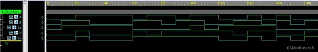
VL20 数据选择器实现逻辑电路
题目描述
请使用此4选1数据选择器和必要的逻辑门实现下列表达式。
L=A∙B+A∙~C+B∙C
数据选择器的逻辑符号如下图:
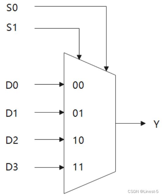
数据选择器代码如下,可在本题答案中添加并例化此数据选择器。
RTL 设计
module data_sel(
   input             S0     ,
   input             S1     ,
   input             D0     ,
   input             D1     ,
   input             D2     ,
   input             D3     ,

   output wire        Y
);

assign Y = ~S1 & (~S0&D0 | S0&D1) | S1&(~S0&D2 | S0&D3);

endmodule

module sel_exp(
   input             A     ,
   input             B     ,
   input             C     ,

   output wire       L
);
    data_sel luoji(
        .S1(A),
        .S0(B),
        .D0(1'b0),
        .D1(C),
        .D2(~C),
        .D3(1'b1),
        .Y(L)
    );
endmodule
testbench 设计
`timescale 1ns/1ns

module tb_sel_exp();
	reg       A;
	reg       B;
	reg       C;
	wire      L;

initial begin
	A <= 1'b0;
	B <= 1'b0;
	C <= 1'b0;
	#200
	$finish;
end

always #10 A <= {$random} % 2'd2;
always #10 B <= {$random} % 2'd2;
always #10 C <= {$random} % 2'd2;

sel_exp sel_exp_inst(
	.A   (A),
	.B   (B),
	.C   (C),
	.L   (L)
	);

//fsdb
initial begin
	$fsdbDumpfile("tb_sel_exp.fsdb");
	$fsdbDumpvars(0);
end

endmodule
VL21 根据状态转移表实现时序电路
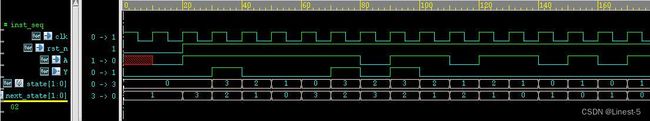
题目描述
某同步时序电路转换表如下,请使用D触发器和必要的逻辑门实现此同步时序电路,用Verilog语言描述。
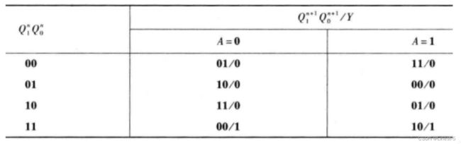
电路的接口如下图所示。

RTL 设计
`timescale 1ns/1ns

module seq_circuit(
      input          clk,
      input          rst_n,
      input          A,
      output  wire   Y
);

reg  [1:0]    state;
reg  [1:0]    next_state;
reg           Y_reg;

//状态机第一段,状态跳转,时序逻辑
always @(posedge clk or negedge rst_n) begin
	if (!rst_n) begin
		state <= 2'b00;
	end
	else begin
		state <= next_state;
	end
end

//状态机第二段,转移条件,组合逻辑
always @(*) begin
	next_state = state;
	case(state)
		2'b00: begin
			if (A == 1'b1) begin
				next_state <= 2'b11;
			end
			else begin
				next_state <= 2'b01;
			end
		end
		2'b01: begin
			if (A == 1'b1) begin
				next_state <= 2'b00;
			end
			else begin
				next_state <= 2'b10;
			end
		end
		2'b10: begin
			if (A == 1'b1) begin
				next_state <= 2'b01;
			end
			else begin
				next_state <= 2'b11;
			end
		end
		2'b11: begin
			if (A == 1'b1) begin
				next_state <= 2'b10;
			end
			else begin
				next_state <= 2'b00;
			end
		end
		default: begin
			next_state <= 2'b00;
		end
	endcase
end

//状态机第三段,结果输出,时序逻辑
always @(posedge clk or negedge rst_n) begin
	if (!rst_n) begin
		Y_reg <= 1'b0;
	end
	else if (next_state == 2'b11) begin
		Y_reg <= 1'b1;
	end
	else begin
		Y_reg <= 1'b0;
	end
end

assign Y = Y_reg;

endmodule
testbench 设计
`timescale 1ns/1ns

module tb_seq_circuit();

	reg       clk;
	reg       rst_n;
	reg       A;
	wire      y;

initial begin
	clk = 1'b1;
	rst_n <= 1'b0;
	#20
	rst_n <= 1'b1;
	#200
	$finish;
end

always #5  clk =  ~clk;
always #10 A   <= {$random} % 2'd2;

seq_circuit inst_seq (
	.clk(clk),
	.rst_n(rst_n),
	.A(A),
	.Y(Y)
);

//fsdb
initial begin
	$fsdbDumpfile("tb_seq_circuit.fsdb");
	$fsdbDumpvars(0);
	$fsdbDumpMDA();
end

endmodule
仿真测试
VL22 根据状态转移图实现时序电路
题目描述
某同步时序电路的状态转换图如下,→上表示“C/Y”,圆圈内为现态,→指向次态。
请使用D触发器和必要的逻辑门实现此同步时序电路,用Verilog语言描述。
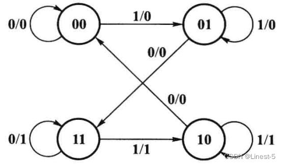
电路的接口如下图所示,C是单bit数据输入端。

RTL 设计
module seq_circuit(
   input         C,
   input         clk,
   input         rst_n,
   output        Y
);

parameter   S0  =  2'b00;
parameter   S1  =  2'b01;
parameter   S2  =  2'b10;
parameter   S3  =  2'b11;

reg  [1:0]   state;
reg  [1:0]   next_state;

//状态机第一段,状态跳转,时序逻辑
always @(posedge clk or negedge rst_n) begin
	if (!rst_n) begin
		state <= S0;
	end
	else begin
		state <= next_state;
	end
end

//状态机第二段,条件转移,组合逻辑
always @(*) begin
	next_state = state;
	case(state)
		S0: begin
			if (C) begin
				next_state = S1;
			end
			else begin
				next_state = S0;
			end
		end
		S1: begin
			if (C) begin
				next_state = S1;
			end
			else begin
				next_state = S3;
			end
		end
		S2: begin
			if (C) begin
				next_state = S2;
			end
			else begin
				next_state = S0;
			end
		end
		S3: begin
			if (C) begin
				next_state = S2;
			end
			else begin
				next_state = S3;
			end
		end
		default: begin
			next_state = S0;
		end
	endcase
end

//状态机第三段,结果输出,组合逻辑
assign Y = ((state==S2) && (C == 1'b1)) || (state == S3);

endmodule
testbench 设计
`timescale 1ns/1ns

module tb_seq_circuit();

reg       C;
reg       clk;
reg       rst_n;
wire      Y;

initial begin
	clk = 1'b1;
	rst_n = 1'b0;
	#20
	rst_n = 1'b1;
	#200
	$finish;
end

always #5   clk = ~clk;
always #10  C  <= {$random} % 2'd2;

seq_circuit inst_seq (
	.C     (C),
	.clk   (clk),
	.rst_n (rst_n),
	.Y     (Y)
);

initial begin
	$fsdbDumpfile("tb_seq_circuit.fsdb");
	$fsdbDumpvars(0);
	$fsdbDumpMDA ();
end

endmodule
VL23 ROM的简单实现
题目描述
实现一个深度为8,位宽为4bit的ROM,数据初始化为0,2,4,6,8,10,12,14。可以通过输入地址addr,输出相应的数据data。
接口信号图如下:

使用Verilog HDL实现以上功能并编写testbench验证。
RTL 设计
module rom(
	input          clk,
	input          rst_n,
	input  [7:0]   addr,

	output [3:0]   data
);

reg [3:0]   rom  [7:0];
reg [3:0]   data_reg;

integer i;
initial begin
	for (i=0;i<8;i=i+1) begin
		rom[i] = i*2;
	end
end

always @(*) begin
	if (!rst_n) begin
		data_reg <= 4'd0;
	end
	else begin
		data_reg <= rom[addr];
	end
end

assign data = data_reg;

endmodule
testbench 设计
`timescale 1ns/1ns

module tb_rom();

reg            clk;
reg            rst_n;
reg  [7:0]     addr;
wire [3:0]     data;

initial begin
	clk    = 1'b1;
	rst_n <= 1'b0;
	#20
	rst_n <= 1'b1;
	#200
	$finish;
end

always #5  clk   = ~clk;
always #10 addr <= {$random} % 4'd8;

rom inst_rom (
	.clk   (clk),
	.rst_n (rst_n),
	.addr  (addr),
	.data  (data)
);

//fsdb
initial begin
	$fsdbDumpfile("tb_rom.fsdb");
	$fsdbDumpvars(0);
	$fsdbDumpMDA();
end

endmodule
VL24 边沿检测
题目描述
有一个缓慢变化的1bit信号a,编写一个程序检测a信号的上升沿给出指示信号rise,当a信号出现下降沿时给出指示信号down。
注:rise,down应为单脉冲信号,在相应边沿出现时的下一个时钟为高,之后恢复到0,一直到再一次出现相应的边沿。
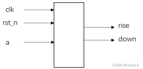
使用Verilog HDL实现以上功能并编写testbench验证。
RTL 设计
module edge_detect(
	input         clk,
	input         rst_n,
	input         a,

	output reg    rise,
	output reg    down
);

reg       a_reg;
wire      pulse;

always @(posedge clk or negedge rst_n) begin
	if (!rst_n) begin
		a_reg <= 1'b0;
	end
	else begin
		a_reg <= a;
	end
end

assign pulse = a ^ a_reg;

always @(posedge clk or negedge rst_n) begin
	if (!rst_n) begin
		rise <= 1'b0;
		down <= 1'b0;
	end
	else if (pulse && a) begin
		rise <= 1'b1;
	end
	else if (pulse && ~a) begin
		down <= 1'b1;
	end
	else begin
		rise <= 1'b0;
		down <= 1'b0;
	end
end

endmodule
testbench 设计
`timescale 1ns/1ns

module tb_edge_detect();
reg        clk  ;
reg        rst_n;
reg        a    ;
wire       rise ;
wire       down ;

initial begin
	clk = 1'b1;
	rst_n <= 1'b0;
	a <= 1'b0;
	#20
	rst_n <= 1'b1;
	#20
	a <= 1'b1;
	#20
	a <= 1'b0;
	#30
	a <= 1'b1;
	#40
	a <= 1'b0;
	#20
	a <= 1'b1;
	#20
	a <= 1'b0;
	#20
	$finish;
end

always #5  clk   = ~clk;

edge_detect inst_edge_detect (
	.clk   (clk),
	.rst_n (rst_n),
	.a     (a),
	.rise  (rise),
	.down  (down)
);

//fsdb
initial begin
	$fsdbDumpfile("tb_edge_detect.fsdb");
	$fsdbDumpvars(0);
	$fsdbDumpMDA();
end

endmodule