Sentaurus TCAD学习之SDE
Sentaurus TCAD学习之Sde
- 分析IGBT例子中SDE代码
分析IGBT例子中SDE代码
; Using DF-ISE coordinate system for structure generation
//使用DF-ISE坐标系生成结构
(sde:set-process-up-direction "+z")
;----------------------------------------------------------------------
; Structure definition (结构定义)
;----------------------------------------------------------------------;
(sdegeo:set-default-boolean "BAB")
//表示新的区域不会覆盖之前旧的区域
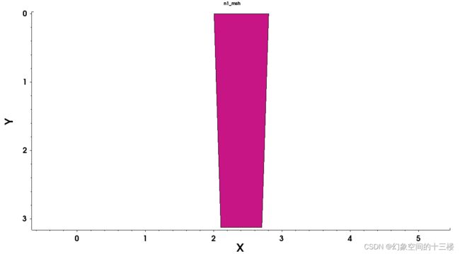
(sdegeo:create-polygon (list
  (position 2.0 0.0 0)
  (position 2.1 3.13 0)
  (position 2.7 3.13 0)
  (position 2.8 0.0 0)
  (position 2.0 0.0 0))
  "PolySi" "R.PolyGate")
//多边形区域画法,画一个梯形,表示多晶硅
(sdegeo:fillet-2d (find-vertex-id (position 2.1 3.13 0)) 0.2)
(sdegeo:fillet-2d (find-vertex-id (position 2.7 3.13 0)) 0.2)
//对棱角进行圆润化处理,在画出的多晶硅梯形下边角两处进行曲线化

(sdegeo:create-polygon (list
  (position 1.98 0.00 0)
  (position 2.08 3.22 0)
  (position 2.72 3.22 0)
  (position 2.82 0.00 0)
  (position 1.98 0.00 0))
  "Oxide" "R.Gox")
/*
填充氧化物,根据之前定义的"BAB",新的区域不会覆盖之前的区域
该区域为氧化物,比之前定义的多晶硅区域稍大,起到隔离作用
*/
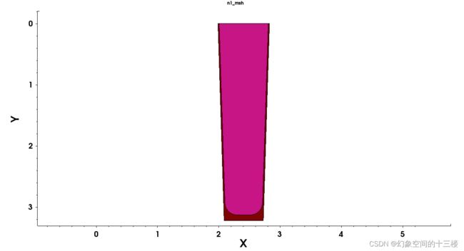
(sdegeo:fillet-2d (find-vertex-id (position 2.08 3.22 0)) 0.2)
(sdegeo:fillet-2d (find-vertex-id (position 2.72 3.22 0)) 0.2)
//同样对下边角两处进行曲线化处理

(sdegeo:create-polygon (list
  (position 2.00  0.02 0)
  (position 1.50  0.02 0)
  (position 1.30  0.22 0)
  (position 0.00  0.22 0)
  (position 0.00 -0.18 0)
  (position 1.30 -0.18 0)
  (position 1.50  0.00 0)
  (position 2.00  0.00 0)
  (position 2.00  0.02 0))
  "Oxide" "R.LOCOS")
//定义氧化物区域
(sdegeo:fillet-2d (find-vertex-id (position 1.3  0.22 0)) 0.15)
(sdegeo:fillet-2d (find-vertex-id (position 1.3 -0.18 0)) 0.15)
//对标记位置处进行曲线化

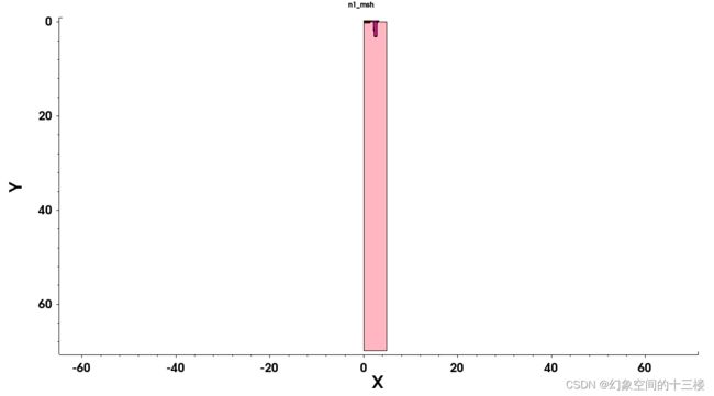
(define xmin 0.0)
(define ymin 0.0)
(define xmax 4.8)
(define ymax 70.0)
//定义x,y方向的最小值
//定义x,y方向的最大值
(sdegeo:create-rectangle
  (position 2.8 -0.3 0.0 )  (position 3.1 0.0 0.0 ) "Oxide"  "R.Spacer" )
//定义氧化物的矩形区域
(sdegeo:create-rectangle
  (position 0.0  0.0 0.0 )  (position 2.8 -0.3 0.0 ) "PolySi"  "R.PolyCont" )
//定义多晶硅的矩形区域
(sdegeo:create-rectangle
  (position 0.0  0.0 0.0 )  (position xmax ymax 0.0 ) "Silicon" "R.Si" )
//定义硅的矩形区域
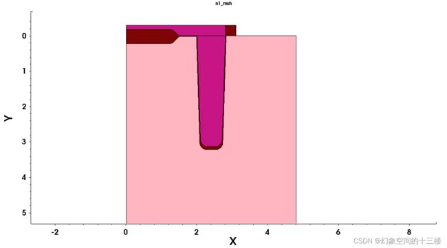
(sdegeo:define-contact-set "Emitter"   4  (color:rgb 1 0 0 ) "##" )
(sdegeo:define-contact-set "Collector" 4  (color:rgb 1 0 0 ) "##" )
(sdegeo:define-contact-set "Gate"      4  (color:rgb 1 0 0 ) "##" )
//定义电极:名称,边缘厚度,颜色
(sdegeo:define-2d-contact (find-edge-id (position 3.5  0.0 0.0)) "Emitter")
(sdegeo:define-2d-contact (find-edge-id (position 3.5 ymax 0.0)) "Collector")
(sdegeo:define-2d-contact (find-edge-id (position 1.0 -0.3 0.0)) "Gate")
//在想要定义电极的地方边缘取一个点
;----------------------------------------------------------------------
; Profiles
;----------------------------------------------------------------------;
; - Substrate
(sdedr:define-constant-profile "Const.Substrate"
"PhosphorusActiveConcentration" 1e+15 )
(sdedr:define-constant-profile-material "PlaceCD.Substrate"
"Const.Substrate" "Silicon" )
//定义衬底的磷浓度为1*10^15,衬底材料为硅
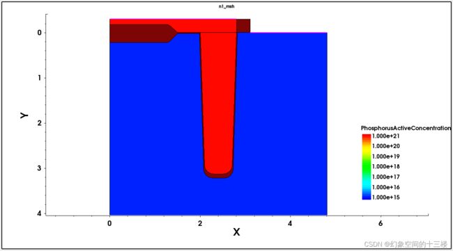
(sdedr:define-constant-profile "Const.PolyGate"
"PhosphorusActiveConcentration" 1e+21 )
(sdedr:define-constant-profile-material "PlaceCD.PolyGate"
"Const.PolyGate" "PolySi" )
//定义栅的磷浓度为1*10^21,栅的材料为多晶硅

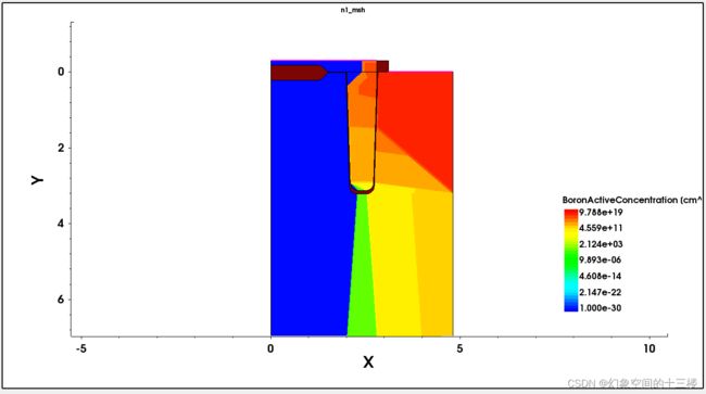
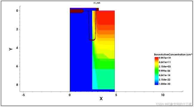
(sdedr:define-refeval-window "BaseLine.pbody" "Line"
 (position 3.0 0.0 0.0)
 (position 5.0 0.0 0.0) )
//定义基准线,掺杂方式为线性掺杂
(sdedr:define-gaussian-profile "Impl.pbodyprof"
 "BoronActiveConcentration"
 "PeakPos" 0.1  "PeakVal" 1e20
 "ValueAtDepth" 1e17  "Depth" 2
 "Erf"  "Length" 0.1)
(sdedr:define-analytical-profile-placement "Impl.pbody"
 "Impl.pbodyprof" "BaseLine.pbody" "Positive" "NoReplace" "Eval")
/*
掺杂类型为高斯掺杂,掺杂元素为硼元素
掺杂浓度的最大值与基准线的距离为0.1
最大浓度是1*10^20
最小浓度是1*10^17
扩散深度为2um
横向扩散长度是0.1um
向正方向扩散
*/
(sdedr:define-refeval-window "BaseLine.nplus" "Line"
 (position 3.0 0.0 0.0)
 (position 3.7 0.0 0.0) )
//定义基准线,掺杂方式为线性掺杂
(sdedr:define-gaussian-profile "Impl.nplusprof"
 "ArsenicActiveConcentration"
 "PeakPos" 0.0  "PeakVal" 1e21
 "ValueAtDepth" 1e17  "Depth" 0.5
 "Erf"  "Length" 0.1)
(sdedr:define-analytical-profile-placement "Impl.nplus"
 "Impl.nplusprof" "BaseLine.nplus" "Positive" "NoReplace" "Eval")
 /*
掺杂类型为高斯掺杂,掺杂元素为砷元素
掺杂浓度的最大值与基准线的距离为0
最大浓度是1*10^21
最小浓度是1*10^17
扩散深度为0.5um
横向扩散长度是0.1um
向正方向扩散
*/

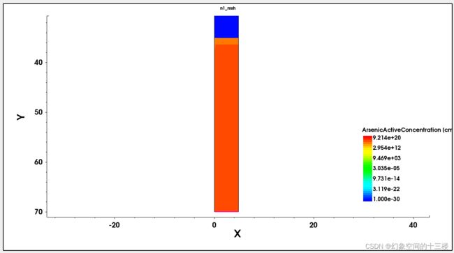
(sdedr:define-refeval-window "BaseLine.fieldstop" "Line"
(position 0.0 70.0 0.0)
(position 5.0 70.0 0.0) )
//定义基准线,掺杂方式为线性掺杂
(sdedr:define-gaussian-profile "Impl.fieldstopprof"
"ArsenicActiveConcentration"
"PeakPos" 0.0 "PeakVal" 1e19
"ValueAtDepth" 1e15 "Depth" 3.0
"Erf" "Length" 0.1)
(sdedr:define-analytical-profile-placement "Impl.fieldstop"
"Impl.fieldstopprof" "BaseLine.fieldstop" "Negative" "NoReplace" "Eval")
/*
掺杂类型为高斯掺杂,掺杂元素为砷元素
掺杂浓度的最大值与基准线的距离为0
最大浓度是1*10^19
最小浓度是1*10^15
扩散深度为3um
横向扩散长度是0.1um
向反方向扩散
*/
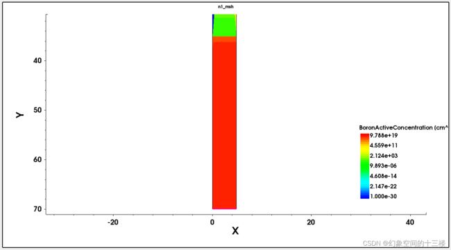
(sdedr:define-refeval-window "BaseLine.collector" "Line"
(position 0.0 70.0 0.0)
(position 5.0 70.0 0.0) )
//定义基准线,掺杂方式为线性掺杂
(sdedr:define-gaussian-profile "Impl.collectorprof"
"BoronActiveConcentration"
"PeakPos" 0.1 "PeakVal" 1e20
"ValueAtDepth" 1e17 "Depth" 0.5
"Erf" "Length" 0.1)
(sdedr:define-analytical-profile-placement "Impl.collector"
"Impl.collectorprof" "BaseLine.collector" "Negative" "NoReplace" "Eval")
/*
掺杂类型为高斯掺杂,掺杂元素为硼元素
掺杂浓度的最大值与基准线的距离为0.1
最大浓度是1*10^20
最小浓度是1*10^17
扩散深度为0.5um
横向扩散长度是0.1um
向反方向扩散
*/
;----------------------------------------------------------------------
; Meshing
;----------------------------------------------------------------------;
(define ds 1)
(sdedr:define-refinement-size "global" (/ 2.5 ds) (/ 10.0 ds) (/ 2.5 ds) 0.1 0.1 0.1 )
//在size中,三个括号和三个0.1表示Xmax Ymax Zmax Xmin Ymin Zmin
(sdedr:define-refeval-window "global" "Rectangle"  (position -1e5 -1e5 0)  (position 1e5 1e5 0) )
(sdedr:define-refinement-placement "global" "global" (list "window" "global" ) )
//list把后面的内容都当做一个元素
(sdedr:define-refinement-size "active_domain" 2.0 5.0 0.5 0.02 0.02 0.05 )
(sdedr:define-refinement-material "active_domain" "active_domain" "Silicon")
(sdedr:define-refinement-function "active_domain" "DopingConcentration" "MaxTransDiff" 1)
(sdedr:define-refinement-function "active_domain" "MaxLenInt" "R.Si" "emitter" 0.002 2 "UseRegionNames")
(sdedr:define-refinement-function "active_domain" "MaxLenInt" "R.Si" "thermo_left" 0.025 2 "UseRegionNames")
(sdedr:define-refinement-function "active_domain" "MaxLenInt" "R.Si" "thermo_right" 0.025 2 "UseRegionNames")
//Defines定义了被使用在Placements部分的精化参数和概要文件定义的集合
//Function按浓度变化;Placement施加网格策略
/*
MaxTransDiff:在元素的顶点处计算剖面的转换值的最大差值。
如果差值大于Value且边长足够大,则元素被细化。

MaxLenInt:这个函数在接口处产生精化。
*/

(sdedr:define-refeval-window "active" "Rectangle"  (position xmin ymin 0.0)  (position xmax ymax 0.0) )
(sdedr:define-refinement-size "active" 1.0 5.0 1.0 0.03 0.02 0.5)
(sdedr:define-refinement-placement "active" "active" "active")
(sdedr:define-refinement-function "active" "DopingConcentration" "MaxTransDiff" 1)

;; Trench Bottom
//沟槽底部
(sdedr:define-refeval-window "RW.TrBot" "Rectangle" (position 1.0 1.8 0.0 ) (position 3.0 4.0 0.0 ))
(sdedr:define-refinement-size "Ref.TrBot" 0.1  0.5 0.05 0.05)
(sdedr:define-refinement-function "Ref.TrBot" "DopingConcentration" "MaxTransDiff" 1)
(sdedr:define-refinement-placement "RefPlace.TrBot" "Ref.TrBot" "RW.TrBot" )


(define nlevels 10)
(define factor 1.5)
//定义nlevels为10,定义factor为1.5

(sdedr:offset-block "material" "Silicon"  "maxlevel" nlevels)
//maxlevel表示在Si中创建10层网格
(sdedr:offset-interface "region" "R.Si" "R.Gox" "hlocal" 0.0015 "factor" factor)
//hlocal表示氧化硅界面处的网格间距为1.5nm
(sdedr:offset-interface "region" "R.Gox" "R.PolyGate" "hlocal" 0.01 "factor" factor)
(sdedr:offset-interface "region" "R.Gox" "R.Si" "hlocal" 0.003 "factor" factor)
/*
定义栅氧中的网格间距,在氧化物-多晶硅界面设置为10nm
在氧化物-硅界面设置设置3nm
Factor定义网格层的网格间距按1.5倍增加
*/
