【ProNoC】Chap.1 ProNoC生成2x2的mesh型的4核片上网络系统;实现NoC的RTL设计
【ProNoC】Chap.1 ProNoC生成2x2的mesh型的4核片上网络系统;实现NoC的RTL设计
- 0. NoC多核片上网络生成器
-
- ProNoC
- ProNoC的功能实现
- 1. 生成一个叫做Mor1kx SoC的单个Tile(包含NI网络接口)
-
- 1.1 打开ProNoC用于生成Tile的GUI界面
- 1.2 为Tile添加时钟IP
-
- 参数类型:localparameter和parameter和Don't include
- 1.3 为Tile添加wishbone总线IP
- 1.4 添加其他的IP:Mor1kx核、RAM、Timer、jtag、GPIO
-
- SoC里的几个IP的分析
- 配置NI网络接口给wishbone总线的SoC
- 1.5 检查SoC上在内存占用的地址映射
- 1.6 检查SoC的功能连接图
- 1.7 为FPGA上定义时钟(不用做)
- 1.8 报错分析 Gtk3::Gdk::Window失效
- 1.9 生成这个基于Mor1kx内核的SoC的RTL代码
- **2. 使用SoC搭建一个4核的片上网络系统**
-
- 2.1 配置一个2x2的mesh型的NoC网络结构,使用xy路由协议
- 2.2 配置NoC网络的各个处理器核/SoC/CPU/GPU/纯内存
- 2.3 从Diagram查看生成的NoC based MPSoC的结构图
- 2.4 另存为mor1k_mpsoc.mpsoc作为配置文件
- 2.5 为FPGA生成时钟(不用做)
- 2.6 生成RTL代码
- 3. NoC based MPSoC 级的软件编程
-
- 3.1 每个Tile的软件程序转译到SoC的RAM里实现功能
-
- main.c在每个Tile里编写
- main.c解析
- 3.2 使用verilater进行编译和仿真
- 3.3 生成Testbench.cpp作为测试文件
-
- Testbench.cpp文件
- 3.4 ==仿真结果==
- 报错
- 4. 综合
-
- 4.1 用quartus ii 综合生成后的Mor1kx的RTL代码
-
- Debug记录
- 4.2 综合2x2的mor1k_mpsoc
0. NoC多核片上网络生成器
实现NoC的RTL设计一直是很复杂的,而NoC生成器(Network-on-Chip Generator)是一种用于设计和生成Network-on-Chip架构的工具。它可以根据用户的需求和参数,如网络的尺寸、拓扑结构、路由算法等,自动生成具有所需特性的NoC设计。主要功能包括自动生成和优化NoC设计以及进行性能分析和验证。简而言之,NoC生成器可以帮助实现更高效且可靠的系统集成设计。
ProNoC
ProNoC有一个很简洁的GUI界面。
- 如果想生成一个SoC,只需要选择内核(有很多种软核)、wishbone总线、内存等IP并设置好参数和大小,ProNoC工具链就可以“连连看”把一个SoC的RTL代码生成出来。ps,未来ChatGPT生成RTL代码指日可待。
- 如果想生成一个MPSoC多核系统,选择期待用到的SoC并用统一的NoC模块连接,因为NI出去之后是Router。NoC的通信即通过Router之间的通信和路由。
- ProNoC甚至提供了可以烧录FPGA的功能。

- ProNoC - User Manual用户手册
- ProNoC - OpenCores
- ProNoC - Github
- ProNoC - User Manual(github的一版)
- ProNoC_System_Overview
- Monemi A, Tang J W, Palesi M, et al. ProNoC: A low latency network-on-chip based many-core system-on-chip prototyping platform[J]. Microprocessors and Microsystems, 2017, 54: 60-74.
ProNoC的功能实现
除了配置NoC的结构,在一个多处理器系统上芯片(MPSoC)中,每个处理器核心(也叫内核)都会有它自己的一份代码,这份代码通常是用C或者其他高级语言编写的。这份代码定义了处理器核心的功能和行为。
在NoC的环境中,这些处理器核心通过网络接口(Network Interface,NI)与网络进行通信。每个内核都有一个或多个NI,这些NI负责将内核的通信需求转化为网络可以理解的消息。
C/C++编程就是描述了每一个内核输出信息的动作,包括输出内容、格式和目的地,然后通过NI(Network Interface)接口输出的标准通信信息(Flits组成Packet)。将C/C++转译为该SoC内核理解的二进制代码存储到RAM里,这些代码描述了内核如何处理数据、执行任务,以及如何通过其网络接口(Network Interface,NI)生成和发送通信信息。

除了每个内核的main.c编程以外,在PC上做仿真时,还需要编写Testbench.cpp(用于Verilator联合仿真)或Testbench.v(modelsim)为测试提供激励。
1. 生成一个叫做Mor1kx SoC的单个Tile(包含NI网络接口)
按照官网用户手册的 《CHAPTER 5. Processing Tile Generator Hello World Tutorial》生成单个Processing Tile以用来搭建多核网络。
1.1 打开ProNoC用于生成Tile的GUI界面
cd ~/ProNoC/mpsoc/perl_gui
perl ./ProNoC.pl
进去以后,在上侧的菜单栏选择“Processing tile generator”。
在左侧的树视图窗口中,您可以看到所有可用 IP 类别的列表。 单击每个类别展开相关的 IP 核列表。 每个 IP 核都可以通过双击其名称添加到 GUI。
- 在第一列中,您可以在 GUI 界面中上下移动 IP 核框位置,移除 IP 核或设置其参数(如果有)。
- 在第二列中,您可以重命名 IP 内核实例名称。
- 第三列显示该模块的所有 (Plug) 接口。 在这里您可以将每个插头连接到一个合适的(插座)接口。 (每个接口分为插头和插座两种类型。有关接口的更多信息,请参阅接口生成器章节。您也可以在此处将接口导出为 SoC 的输入/输出 (IO) 端口。
1.2 为Tile添加时钟IP
- 在左侧 “IP list” 里选择:Source 双击clk_source即可添加时钟IP
- 并重命名第二列的“Instance Name”为:`clk_source。
- 将clk和reset的类型选择为==
IO==。

参数类型:localparameter和parameter和Don’t include
在设置IP的时候可以看到,参数的选项有三个:localparameter和parameter。
localparam和parameter是Verilog硬件描述语言中的两个关键字,它们都用于定义参数,但在用法和应用场景上有所不同。
parameter是Verilog中的常数,一般用于模块间传参,即允许在实例化模块的时候设置参数的值。这就意味着,如果你选择把它定义为parameter,那么在网络-on-chip(NoC)基础上的MPSoC生成时,你就可以更改处理tile参数的值,允许在不同地方以不同的参数值调用相同的tile。
与此相反,localparam定义的是局部参数,这些参数不能从模块外部更改。一旦在模块内部被定义,它们的值就固定了,无法在模块实例化时更改。
所以,何时使用localparam和parameter主要取决于你的需求:
- 如果你需要在你的network-on-chip(NoC)设计中,为相同的处理tile实例赋予不同的参数值,那么应该使用
parameter。 - 如果你有一些固定的参数值,这些值在定义后不需要更改,或者你不希望这些值被外部模块更改,那么应该使用
localparam。
关于"不包括"(Don’t include)的选择,如果参数是一个需要在软件代码中使用的软件参数,你可以选择这个选项。这样,参数将不会在生成的Verilog文件中被定义,而是在软件代码中定义和使用。
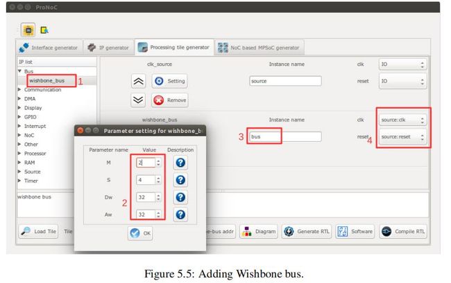
1.3 为Tile添加wishbone总线IP
双击Bus底下的wishbone_bus可添加重新命名为wishbone_bus,都选为localparam并设为如下参数
-
M是master interfaces number,设为4;其中分别为:内核的instruction write back、内核的data write back、Network Interface的wb_send、Network Interface的wb_receive;
-
S是slave interfaces number,设为4;其中分别为RAM的wb、Network Interface的wb_slave、timer的wb、uart的wb;
-
Dw是Data width,设为32;
-
Aw是Address width,设为32;
1.4 添加其他的IP:Mor1kx核、RAM、Timer、jtag、GPIO
按照下图设置:图片里的名字没有完全对上,比如clk_source:clk;
官方文档图里标黄的地方的slave的号没对上,我这里设置了:
-
slave[0]连RAM
-
slave[1]连NI
-
slave[2]连Timer
-
slave[3]连uart

-
M是master interfaces number,设为4;其中分别为:内核的instruction write back、内核的data write back、Network Interface的wb_send、Network Interface的wb_receive;
-
S是slave interfaces number,设为4;其中分别为RAM的wb、Network Interface的wb_slave、timer的wb、uart的wb;
设置后如图所示,参数类型我都选的localparam


SoC里的几个IP的分析
值得注意的是,
- 在Processer的Mor1kx核设置时:iwb(instruction write back)连上了wishbone总线的**master[0]**口;(wishbone_bus:wb_master[0])
- 在Processer的Mor1kx核设置时:dwb(data write back)连上了wishbone总线的**master[1]**口(wishbone_bus:wb_master[1]);
- 在单端口RAM的设置中:wb(write back)连上了wishbone总线的**slave[0]**口(wishbone_bus:wb_slave[0]);
- 在NI网络接口的设置中:wb_send连上了wishbone_bus:wb_master[2];wb_receive连上了wishbone_bus:wb_master[3];wb_slave连上了wishbone_bus:wb_slave[1]; interrupt连上了mrk1kx核的中断口[1](mor1kx:interrupt_peripheral[0]);
- 在Timer定时器的设置中:wb(write back)连上了wishbone总线的**slave[2]**口(wishbone_bus:wb_slave[2]); intrp(interrupt)连上了mrk1kx核的中断口[1](mor1kx:interrupt_peripheral[1]);
- 在ProNoC_jtag_uart(实例名字叫uart)的设置中,wb_slave连上了wishbone总线的**slave[3]**口(wishbone_bus:wb_slave[3]);
配置NI网络接口给wishbone总线的SoC
请注意,本章中所需的磁贴具有要连接到 NoC 的网络接口 (NI) IP。
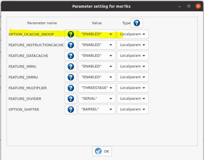
- NI 有一个主接口,可以自动将NoC 到达的数据包写入主存储器。
- 因此,对于启用了数据缓存的 CPU,您需要支持探听(以使 NI 写入的数据缓存内存位置无效)或将 NI 接收器缓冲区映射到不可缓存的内存位置。
- 对于这个例子,我们启用了 Mor1kx 处理器的监听支持。 CPU的snoop接口必须连接到WB,通知主存数据变化。
1.5 检查SoC上在内存占用的地址映射
添加所有需要的 IP 内核后,现在您可以通过单击 Wishbone-bus addr 按钮是==WB addr==检查自动分配的 Wishbone 总线地址。这些地址是根据 IP 内核库设置、插入的参数和系统中重复的相同 IP 内核的数量自动设置的。 但是,您可以随意将它们调整为新值,因为插入的地址没有冲突。
我使用了默认的值。

ps, instance name前的那个序号0:uart的序号顺序好像没什么影响。
1.6 检查SoC的功能连接图
点击 Diagram 按钮观察 SoC 功能框图,上面有三个选项:移除未连接的实例、移除clk的连接、移除reset的连接。可以得到下图的连接关系,很方便。

1.7 为FPGA上定义时钟(不用做)
如果计划将处理块用于MPSoC 内的内部模块,则可以忽略时钟设置。
如果希望SoC成为FPGA实现中的顶层模块(例如,在此示例生产的RTL代码),您可能需要从 FPGA 输入参考时钟生成 SoC 时钟信号。
为此,请单击 CLK 设置按钮。 它将打开一个新窗口,您可以在其中将 SoC 顶级模块连接到某些时钟源。 例如 Xilinx Kintex-7 FPGA KC705 有一个差分参考时钟。 首先需要使用 IBUFGDS 模块将差分 FPGA 输入时钟转换为单个时钟。 IBUFGDS (diff:clk) 的输出为 200 MHz,对于所需的 SoC 来说太高了,无法满足时序约束。 该时钟可以使用 PLL 进行二分频。 为此,将 PLL 倍频 (CLKFBOUT_MULT) 和分频因子 (CLKOUT0_DEVIDE) 分别设置为 9 和 18
-
请注意,如果您希望直接将FPGA 参考时钟连接到SoC,则可以省略此配置。 TOP 模块的时钟和复位信号默认保留为输出。
-
如果计划将处理块用于MPSoC 内的内部模块,则可以忽略时钟设置。
1.8 报错分析 Gtk3::Gdk::Window失效
报错记录:我在使用gui生成tile的时候选择参数有弹出窗口,点击“X”关闭弹出的窗口之后发现gui界面里的一部分设置界面没了,然后报这个错误。
报错描述
perl ./ProNoC.pl
***  unhandled exception in callback:
***  undef is not of type Gtk3::Gdk::Window at /usr/lib/x86_64-linux-gnu/perl5/5.30/Glib/Object/Introspection.pm line 67.
***  ignoring at /home/ubuntu/perl5/lib/perl5/Gtk3.pm line 572.
报错分析:当你关闭GUI窗口时,GTK3的窗口和相关的资源会被自动销毁。如果你在这之后尝试访问这些资源(比如,调用一个方法或者获取一些属性),你会遇到这个错误,因为你正在试图操作一个不存在的窗口。
尝试解决方法:
- 如果是在输入perl ./ProNoC.pl直接打不开gui界面且报这个错误,请尝试用ubuntu20.04系统而不是22.04。(亲测有效)
- 在关闭弹出的窗口时尽量点“ok”而不是右上角的“x”,让回调函数可以往回去传值而不是中止函数运行。
- 出现了错不要慌,把现有的设置先保存下来,下次再打开的时候,直接load file,可以省略很多步骤。

1.9 生成这个基于Mor1kx内核的SoC的RTL代码
-
设置Tile名称为==
mor1k_tile==。 -
按
Generate RTL按钮生成这个Tile的RTL代码。

至此,一个Tile已经搭建完毕了。接下来尝试搭建2x2的NoC网络。
2. 使用SoC搭建一个4核的片上网络系统
在官网用户手册第七章《CHAPTER 7. Simple message passing demo on 2×2 MPSoC》
按照下图,使用我们做好的这个Tile搭建NoC网络。

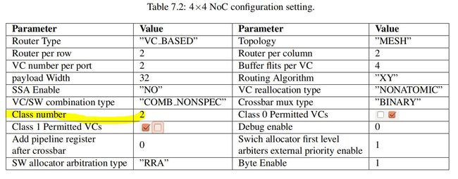
2.1 配置一个2x2的mesh型的NoC网络结构,使用xy路由协议
重新启动ProNoC用于生成Tile的GUI界面。进去以后,在上侧的菜单栏选择“NoC based MPSoC generator”。
cd ~/ProNoC/mpsoc/perl_gui
perl ./ProNoC.pl

- 上图的minimum packet size 应为3
按照表 7.2 设置 NoC 配置设置。 在这里,我们定义了两个虚拟网络 (VN, Virtual Network),方法是定义两个消息类别并分离消息类别允许的 VC,每个消息类别只能使用其自己的专用 VC。
2.2 配置NoC网络的各个处理器核/SoC/CPU/GPU/纯内存
在Tile configuration setting里设置Tile的类型,每个Tile是我们自己的添加进去的核,一般自动生成的会放在lib/soc底下。
您应该能够看到在其共享总线中具有 NI IP 核的所有处理 tile 模块的列表,在这里设置NoC网络里各种各样的核是什么,将 Mor1k_tile设置为 0,1,2,3或简单地设置为 0:3。即,NoC网络具有16个SoC,每个SoC的类型是Mor1k_tile。也可以通过简单地单击 NoC GUI界面上的在各个位置上的Tile,将生成的处理Tile映射到它们的位置。

按下 OK 按钮,它会显示一个窗口,您可以在其中更改默认参数值。具有自定义参数设置的磁贴在其名称上标有 *。
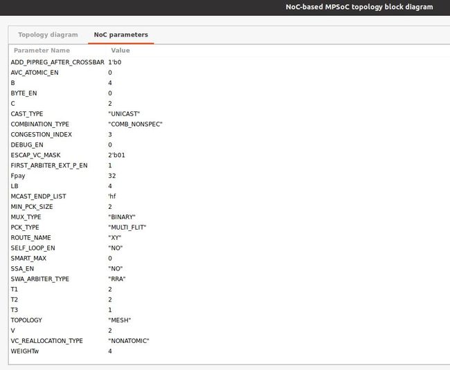
2.3 从Diagram查看生成的NoC based MPSoC的结构图
点击Diagram按钮查看结构框图如下:

还可以查看NoC网络的参数
2.4 另存为mor1k_mpsoc.mpsoc作为配置文件

2.5 为FPGA生成时钟(不用做)
同1.7所讲
如果应使用 FPGA clk 引脚生成 MPSoC clk,请单击 CLK
设置按钮然后跟随 CLK 设置以生成 MPSoC 时钟。
2.6 生成RTL代码
Click on Generate RTL button to generate the MPSoC RTL code.

3. NoC based MPSoC 级的软件编程
3.1 每个Tile的软件程序转译到SoC的RAM里实现功能
-
点击
software进行软件编程使用C代码 -
在左边的Tree-View窗口中,可以选择工程sw目录下的任意一个文件打开,然后进行编辑。 用以下 C 代码替换所有图块中 main.c 文件的内容。
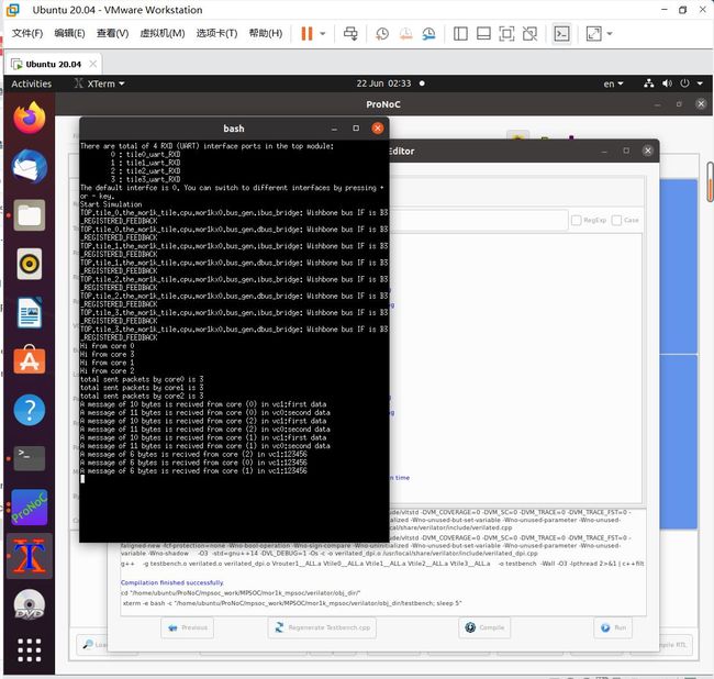
在此示例中,tile 0 到 2 将每 3 个数据包发送到 tile 3。 tiles 3 显示串口终端中的数据包内容。

main.c在每个Tile里编写
直接复制粘贴到每个Tile里的main函数上。现在按下编译按钮。 这使用 Mor1kx GNU 工具链编译 C 代码。 如果一切运行正常,您一定会看到“编译成功完成”消息。 否则,请检查错误消息以修复您的代码并再次按下编译按钮。
#define MULTI_CORE
#include "mor1k_tile.h"

unsigned char pck1[10] = "first data";
unsigned char pck2[11] = "second data";
unsigned char pck3[6] = "123456";
unsigned char receive_buff[ni_NUM_VCs][16];

// a simple delay function
void delay(unsigned int num) {
    while (num > 0) {
        num--;
        nop();
    }
}

void error_handelling_function() {
    unsigned int i;
    for (i = 0; i < ni_NUM_VCs; i++) {
        if (ni_got_buff_ovf(i)) {
            printf("VC%u: The receiver allocated buffer size is smaller than the received packet size in core%u\n", i, COREID);
            ni_ack_buff_ovf_isr(i);
        }
        if (ni_got_send_dsize_err(i)) {
            printf("VC%u: The send data size is not set in core%u\n", i, COREID);
            ni_ack_send_dsize_err_isr(i);
        }
        if (ni_got_burst_size_err(i)) {
            printf("VC%u: The burst size is not set in core%u\n", i, COREID);
            ni_ack_burst_size_err_isr(i);
        }
        if (ni_got_invalid_send_req(i)) {
            printf("VC%u: A new send request is received while the DMA is still busy sending the previous packet in core%u\n", i, COREID);
            ni_ack_invalid_send_req_isr(i);
        }
        if (ni_got_crc_mismatch(i)) {
            printf("VC%u: CRC mismatched in core%u\n", i, COREID);
            ni_ack_crc_mismatch_isr(i);
        }
    }
}

void got_packet_funtion(void) {
    unsigned int i;
    // unsigned char iport;
    for (i = 0; i < ni_NUM_VCs; i++) {
        if (ni_got_packet(i)) {
            // iport = ni_RECEIVE_PRECAP_DATA_REG(i);
            // different destination can be targeted according to iport value
            // E.g if (iport == 0) ini_receive(i, (unsigned int)&receive_buff_p0[i][0], 16, 0);
            // E.g else if (iport == 1) ini_receive(i, (unsigned int)&receive_buff_p1[i][0], 16, 0);
            ni_receive(i, (unsigned int)&receive_buff[i][0], 16, 0);
            ni_ack_got_pck_isr(i);
        } // If ni got packet
    }
}

void check_packet_funtion(void) {
    // unsigned char iport;
    unsigned int i, j, size;
    struct SRC_INFOS src_info;
    for (i = 0; i < ni_NUM_VCs; i++) {
        if (ni_packet_is_saved(i)) {
            src_info = get_src_info(i);
            size = ni_RECEIVE_DATA_SIZE_REG(i);  // size in bytes
            // iport = src_info.r;
            // run a function on the received packet according to the destination port
            // E.G func_on_received_packet(iport);
            // but here we just print the received packet in the terminal
            printf("A message of %u bytes is received from core (%x) in vc%u:", size, src_info.addr, i);
            for (j = 0; j < size; j++) {
                printf("%c", receive_buff[i][j]);
            }
            printf("\n");
            ni_ack_save_done_isr(i);
        } // If ni_packet_is_saved
    }
}

void sent_packet_done_funtion(void) {
    // unsigned char oport;
    unsigned int i;
    for (i = 0; i < ni_NUM_VCs; i++) {
        if (ni_packet_is_sent(i)) {
            ni_ack_send_done_isr(i);
        } // If ni_packet_is_sent
    }
}

// NI interrupt function
void ni_isr(void) {
    // place your interrupt code here
    if (ni_any_err_isr_is_asserted()) {
        // An error occurred
        error_handelling_function();
    }
    if (ni_any_sent_done_isr_is_asserted()) {
        // check which VC has finished sending the packet.
        sent_packet_done_funtion();
    }
    if (ni_any_save_done_isr_is_asserted()) {
        // check which VC has finished saving the packet. This function must be called before got_packet_funtion
        check_packet_funtion();
    }
    if (ni_any_got_pck_isr_is_asserted()) {
        // check which VC got packet
        got_packet_funtion();
    }
    return;
}

int main() {
    printf("Hi from core %u\n", COREID);
    general_int_init();
    general_int_add(ni_INT_PIN, ni_isr, 0); // ni_INT_PIN
    // Enable ni interrupt (it's connected to interrupt pin 0)
    general_int_enable(ni_INT_PIN);
    general_cpu_int_en();
    // hw interrupt enable function:
    // ni_initial(burst_size, errors_int_en, send_int_en, save_int_en, got_pck_int_en)
    ni_initial(16, 1, 1, 1, 1); // enable the interrupt when a packet is received, saved, or any error occurs
    if (COREID == 3) while (1); // Core 3 only receives packets from other cores

    ni_transfer(1, 0, 0, 0, (unsigned int)&pck1[0], 10, PHY_ADDR_ENDP_3);
    ni_transfer(1, 1, 1, 0, (unsigned int)&pck2[0], 11, PHY_ADDR_ENDP_3);
    ni_transfer(1, 0, 0, 0, (unsigned int)&pck3[0], 6, PHY_ADDR_ENDP_3);

    printf("Total sent packets by core %u is %u\n", COREID, 3);

    while (1) {
    }
    return 0;
}
main.c解析
这个C语言程序是一个多核(MULTI_CORE)并行计算的程序,针对网络接口(Network Interface,简称NI)进行操作。该程序中使用了MOR1K开放源代码RISC(减少指令集计算)处理器的Tile设备驱动程序。处理器的每一个核心(core)被分配了一个ID(COREID)用于标识。
代码的主要部分可以分为几个模块:
- 全局变量的定义:在最开始的部分,定义了几个全局变量,如
pck1,pck2和pck3是需要发送的数据包,receive_buff是一个二维数组,用于存储每个虚拟通道(VC)接收的数据包。数据包大小被设定为16字节。 - 辅助函数的定义:定义了几个辅助函数,用于处理各种事件,如错误处理(
error_handelling_function),数据包接收(got_packet_funtion),数据包检查(check_packet_funtion)以及数据包发送完成(sent_packet_done_funtion)等。 - 中断处理函数:定义了一个网络接口中断处理函数(
ni_isr),当中断发生时,它会调用上述的辅助函数来处理事件。中断可能发生在以下几种情况:接收到新的数据包,数据包保存完成,数据包发送完成,以及出现错误等。 - main函数:在main函数中,首先初始化并启用了一些基础设置(如打开中断和网络接口)。然后根据COREID的值来决定是否发送数据包。如果COREID等于3,那么这个核心将只接收数据包,不会发送任何数据包。否则,它将会发送数据包
pck1,pck2和pck3。最后进入一个空的无限循环。
该代码的主要作用是在多核环境下,利用网络接口进行数据包的发送和接收。其中有一些硬件特定的函数和变量(如COREID,ni_transfer,general_cpu_int_en等),可能需要特定的硬件环境和库才能正确编译和运行。
3.2 使用verilater进行编译和仿真
如果您的系统上安装了 Verilator 软件,您可以在运行您开发的软件时模拟您的 SoC。 为此,请遵循以下说明:
按下右下角的 Compile RTL 按钮。 这应该打开“选择编译器窗口”,如图 5.17 所示。 选择 Verilator 作为编译器工具,然后按Next。

使用verilator仿真,同时可以把四个核一起仿真。看到如下提示,再点Next
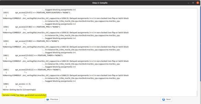
Veriator model has been generated successfully!
- Varilator仿真的一些解释
这个 Vtile0 类是由 Verilator 从 Verilog 硬件描述语言生成的。通常,这个类会在一个 Verilator 生成的硬件模型中被用到,模型的目标是模拟硬件的行为。具体地,当你有一个使用 Verilog 描述的硬件设计(比如说,一个电路或者一个系统芯片),你可以使用 Verilator 工具将其转换成 C++ 代码。这种转换让你可以在一台普通的电脑上模拟硬件的行为,而不需要任何实际的硬件。
3.3 生成Testbench.cpp作为测试文件
在点完Next之后,需要点Regenerate Testbench.cpp生成测试文件。这段代码是一个Verilog硬件仿真的测试平台,用于在C++环境下测试ProNoC 。主要功能包括模拟时钟信号、重置信号、使能信号等,并通过仿真的方式,测试一些硬件模块的功能。
我看了一下代码,这个很像modelsim的功能仿真,只产生时钟、初始化、连接dut。
我们已经把在NoC中发送信息的代码写到了每个Tile的main.c,这个testbench只提供时钟、reset、初始化信号等。然后打印信息。如果没成功输出结果,很可能是因为SoC、MPSoC的参数设置有问题,也可能是Tile里的RAM的地址不匹配。

现在您必须在软件代码编辑窗口中打开 testbech.cpp,如图 5.19 所示。 这是运行生成的 SoC 的最小测试台文件。 它具有连接到时钟和复位信号的 SoC 实例模块。 您可以根据需要编辑此文件。
testbech.cpp这段代码是使用Verilog硬件描述语言(HDL)模拟四个并联的"tile"或硬件模块的C++测试平台。这些"tile"可能是一些处理器,它们被连接在一起,形成一个网络。

Testbench.cpp文件
#include 3.4 仿真结果
在此示例中,tile 0 到 2 将每 3 个数据包发送到 tile 3。 tiles 3 显示串口终端中的数据包内容。
得到的输出结果:
报错
- 替换函数名错误;
testbench.cpp: In function void clk_negedge_event():
testbench.cpp:189:2: error: topology_connect_all_nodes was not declared in this scope; did you mean topology_connect_all_nodes_old?
  189 |  topology_connect_all_nodes ();
      |  ^~~~~~~~~~~~~~~~~~~~~~~~~~
      |  topology_connect_all_nodes_old
make: *** [/usr/local/share/verilator/include/verilated.mk:255: testbench.o] Error 1

Compilation failed.
更改代码片段:
void clk_negedge_event(void){
```
clk = 0;
topology_connect_all_nodes_old();
connect_clk_reset_en_all();
sim_eval_all();
- 没有这个函数
update_router_st(unsigned int, unsigned int, unsigned char*)'
在Testbench.cpp里加这个函数,让编译通过。
void update_router_st(unsigned int param1, unsigned int param2, unsigned char* param3) {
    // 暂时不做任何事
}
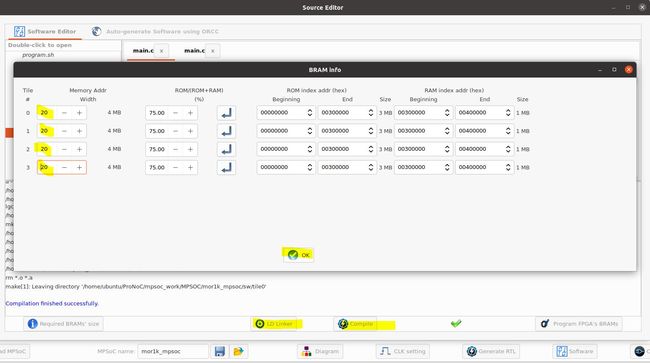
- 更改每一个Tile的RAM的地址大小报错
这种报错。请注意,如果您遇到 RAM 或 ROM 溢出错误,您可以按照链接器 LD 设置修复它们。 如果一切运行成功,您的 sw/tile[n]/RAM 目录中必须有 ram0.bin、ram0.hex 和 ram0.mif 文件,其中 n 是磁贴编号。
The default interfce is 0. You can switch to different interfaces by pressing + or - key.
Start Simulation
Error: The wishbon bus reserved address range width (         14) should be larger than ram width (         20): TOP.tile_0.the_mor1k_tile.ram
%Error: ../src_verilog/lib//./wb_single_port_ram.v:94: Verilog $stop
Aborting...
bash: line 1:  4049 Aborted                 (core dumped) /home/ubuntu/ProNoC/mpsoc_work/MPSOC/mor1k_mpsoc/verilator/obj_dir/testbench
或者这种:
/home/ubuntu/ProNoC/mpsoc_work/toolchain/or1k-elf/bin/or1k-elf-ld: image section `.stack' will not fit in region `ram' /home/ubuntu/ProNoC/mpsoc_work/toolchain/or1k-elf/bin/or1k-elf-ld: region `ram' overflowed by 532 bytes make[1]: *** [Makefile:54: image] Error 1 make: *** [Makefile:5: tile1/.] Error 2

Compilation failed.
这个错误信息是链接器(ld)告诉你 .stack 区段不会适应 ram 区域,这意味着你的程序尝试使用的 RAM 超出了为其分配的空间。错误还告诉你 ram 区域溢出了 532 字节,这可能是因为你的程序中的全局变量、静态变量或者函数调用堆栈等所占用的空间超出了 RAM 的容量。增加 RAM 区域大小:你可以在链接脚本中增加 RAM 区域的大小,如果硬件允许的话。记得之前Tile设置的是20嘛,他俩得对应起来。
4. 综合
4.1 用quartus ii 综合生成后的Mor1kx的RTL代码
可以看到生成的一个Tile是基于wishbone总线,使用Mor1kx内核的SoC,RTL代码很符合规范且可以综合,说明可以用RTL进行下一步FPGA板级验证、门级网表综合

Debug记录
- Error (10054): Verilog HDL File I/O error at output_ports.sv(1): can’t open Verilog Design File “pronoc_def.v”
把所有报错的地方: `include "pronoc_def.v" 换成 `include "./lib/pronoc_def.v"
- Error (10839): Verilog HDL error at noc_localparam.v(36): declaring global objects is a SystemVerilog feature
把noc_localparam.v的文件名改成noc_localparam.sv再加入到quartus里

再把lib/src_noc/pronoc_pkg.sv里的定义`include "noc_localparam.v"改成`include "noc_localparam.sv"
- Error (10644): Verilog HDL error at debug.v(637): this block requires a name
把这部分第637行改成
genvar i;
generate
for (i=0;i-
Error (10052): Verilog HDL error at mor1k_tile_top.sv(275): can’t find port “clk_source_clk_in”
把这部分代码,注释掉子模块里没有的端口,276行
	the_mor1k_tile
	(
		.uart_jtag_to_wb(uart_jtag_to_wb),
		.uart_wb_to_jtag(uart_wb_to_jtag),
		.cpu_cpu_en(cpu_cpu_en & jtag_cpu_en),
		.ni_chan_in(ni_chan_in),
		.ni_chan_out(ni_chan_out),
		.ni_current_e_addr(ni_current_e_addr),
		.ni_current_r_addr(ni_current_r_addr),
		.ram_jtag_to_wb(ram_jtag_to_wb),
		.ram_wb_to_jtag(ram_wb_to_jtag),
		//.clk_source_clk_in(TOP_clk_source_clk_in ),
		//.clk_source_reset_in(TOP_clk_source_reset_in | jtag_system_reset)

	);
-
Error (10232): Verilog HDL error at ni_master.sv(829): index 63 cannot fall outside the declared range [31:0] for vector “m_send_dat_i”
根据报错,给定明确的定义范围[31:0]
       // assign tail_flit_out   =  m_send_dat_i [Fpay-1 : 0];
		 assign tail_flit_out   =  m_send_dat_i [31 : 0];
- Error (10232): Verilog HDL error at ni_master.sv(1047): index 63 cannot fall outside the declared range [31:0] for vector “m_send_dat_i”
                                      (send_tail)? tail_flit_out :  m_send_dat_i [Fpay-1 : 0];
                                      (send_tail)? tail_flit_out :  m_send_dat_i [31 : 0];
- Error (10232): Verilog HDL error at ni_vc_wb_slave_regs.v(404): index 46 cannot fall outside the declared range [31:0] for vector “s_dat_i”
//                        if (send_fsm_is_ideal) hdr_data_next = s_dat_i [HDw-1 : 0];
                        if (send_fsm_is_ideal) hdr_data_next = s_dat_i [31 : 0];
- Error (12006): Node instance “bse2_inst” instantiates undefined entity “BSCANE2”
把这一段代码注释掉mor1k_tile\src_verilog\lib\jtag_wb\xilinx_jtag_wb.v里
/*
    BSCANE2 #(
        .JTAG_CHAIN(JTAG_CHAIN) // Value for USER command.
    )
    bse2_inst
    (
        .CAPTURE(capture), // 1-bit output: CAPTURE output from TAP controller.
        .DRCK( ), // 1-bit output: Gated TCK output. When SEL is asserted, DRCK toggles when CAPTURE or SHIFT are asserted.
        .RESET(tlr), // 1-bit output: Reset output for TAP controller.
        .RUNTEST(), // 1-bit output: Output asserted when TAP controller is in Run Test/Idle state.
        .SEL(sel), // 1-bit output: USER instruction active output.
        .SHIFT(shift), // 1-bit output: SHIFT output from TAP controller.
        .TCK(tck), // 1-bit output: Test Clock output. Fabric connection to TAP Clock pin.
        .TDI(tdi), // 1-bit output: Test Data Input (TDI) output from TAP controller.
        .TMS( ), // 1-bit output: Test Mode Select output. Fabric connection to TAP.
        .UPDATE(update), // 1-bit output: UPDATE output from TAP controller
        .TDO(tdo) // 1-bit input: Test Data Output (TDO) input for USER function.
    );
   */
4.2 综合2x2的mor1k_mpsoc
代码Dubug过程和上面一样。可以看到noc_top模块连着四个tile.
