Xilinx 7系列FPGA config设计文档
xilinx FPGA由于掉电擦除的特性,需要每次上电加载配置文件,具体的配置路径有三种,通过jtag来进行下载,通过FLASH来下载,以及通过外部的处理器来下载( such as a microprocessor, DSP processor, microcontroller, PC, or board tester)。具体配置模式如下:
• Master-Serial configuration mode
• Slave-Serial configuration mode
• Master SelectMAP (parallel) configuration mode (x8 and x16)
• Slave SelectMAP (parallel) configuration mode (x8, x16, and x32)
• JTAG/boundary-scan configuration mode
• Master Serial Peripheral Interface (SPI) flash configuration mode (x1, x2, x4)
• Master Byte Peripheral Interface (BPI) flash configuration mode (x8 and x16) using
parallel NOR flash
配置模式的选择是通过multifunction Pin来决定的,M2,M1,M0, should be set at a
constant DC voltage level, either through pull-up or pull-down resistors (≤ 1 kΩ), or tied
directly to ground or VCCO_0.
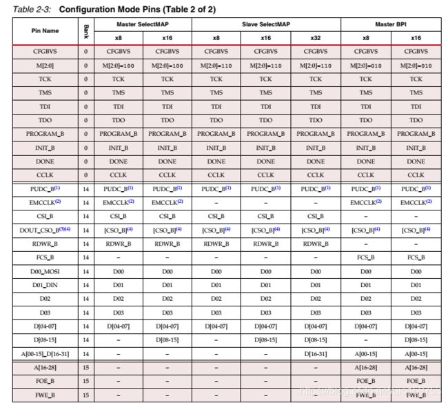
具体配置模式表如下:

考虑到具体配置使用的时候很多管脚并没有用,因此贴下配置的具体的管脚对应表

![]()
![]()
具体的配置的电路图如下
JTAG单一器件配置电路图

多器件的jtag链电路图

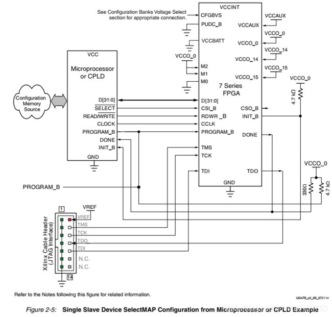
作为从设备串行配置电路图,
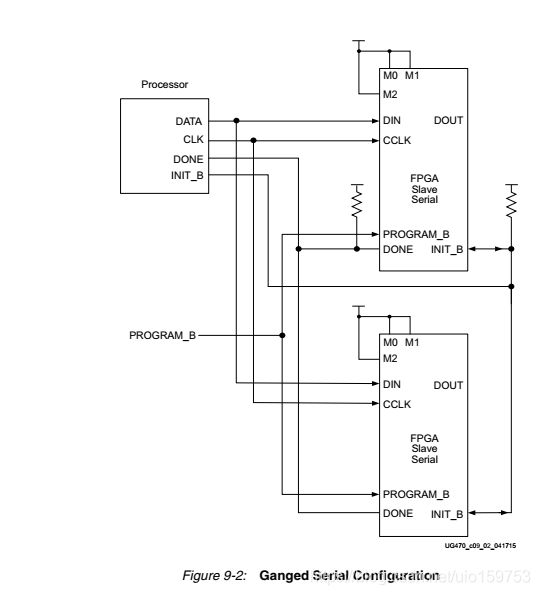
从设备串行链配置电路图

作为从设备并行数据配置电路图,
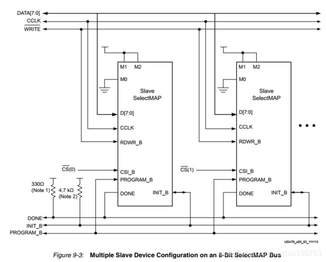
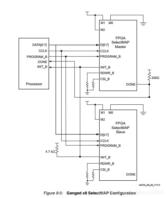
多器件通过8bit select MAP配置电路图
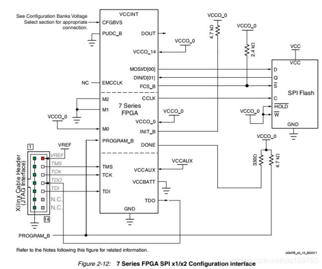
SPI flash配置电路图
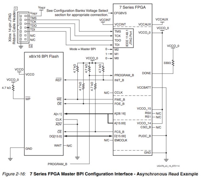
BPI flash异步读取电路图
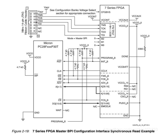
BPI flash同步读取电路图
并行菊花链配置方式(第一个通过flash配置,第二个开始通过串行菊花链配置)

多器件配置相同bit文件电路图
配置管脚具体信息和连接注意事项
| Pin Name |
Bank(1) |
Type |
Direction |
Description |
描述 |
| CFGBVS |
0 |
Dedicated |
Input |
Configuration Banks Voltage Select CFGBVS determines the I/O voltage operating range and voltage tolerance for the dedicated configuration bank 0 and for the multi-function configuration pins in banks 14 and 15 in the Spartan-7, Artix-7 and Kintex-7 families. CFGBVS selects the operating voltage for the dedicated bank 0 at all times in all 7 series devices. CFGBVS selects the operating voltage for the multi-function configuration banks 14 and 15 only during configuration. Connect CFGBVS High or Low per the bank voltage requirements. If the VCCO_0 supply for bank 0 is supplied with 2.5V or 3.3V, then the CFGBVS pin must be tied High (i.e. connected to VCCO_0). Tie CFGBVS to Low (i.e. connected to GND), only if the VCCO_0 for bank 0 is less than or equal to 1.8V. If used during configuration, banks 14 and 15 should match the VCCO level applied to bank 0. Caution! To avoid device damage, CFGBVS must be connected correctly to either VCCO_0 or GND. See Configuration Banks Voltage Select, page 32 for more information. Note: The CFGBVS pin is not available on Virtex-7 HT devices. Virtex-7 HT devices support only 1.8V/1.5V operation for bank 0. |
用来决定bank0和bank14、15的配置管脚的电压范围 如果bank0是2.5V或3.3V供电,则接高电平 如果1.8V供电,接低电平 |
| M[2:0] |
0 |
Dedicated |
Input |
Configuration Mode M[2:0] determine the configuration mode. See Table 2-3, page 23 for the configuration mode settings. Connect each mode pin either directly, or via a ≤ 1 kΩ resistor, to VCCO_0 |
配置模式引脚,见表2.1,一般强上拉1k电阻 |
| TCK |
0 |
Dedicated |
Input |
IEEE Std 1149.1 (JTAG) Test Clock Clock for all devices on a JTAG chain. Connect to Xilinx cable header's TCK pin. Treat as a critical clock signal and buffer the cable header TCK signal as necessary for multiple device JTAG chains. If the TCK signal is buffered, connect the buffer input to an external weak (e.g. 10 kΩ) pull-up resistor to maintain a valid High when no cable is connected. |
tck信号,仿真器给出,如果这个信号接了buffer,那么,buffer的输入接10K的电阻进行弱上拉, |
| TMS |
0 |
Dedicated |
Input |
JTAG Test Mode Select Mode select for all devices on a JTAG chain. Connect to Xilinx cable header's TMS pin. Buffer the cable header TMS signal as necessary for multiple device JTAG chains. If the TMS signal is buffered, connect the buffer input to an external weak (e.g. 10 kΩ) pull-up resistor to maintain a valid High when no cable is connected. |
tms信号,具体同tck |
| TDI |
0 |
Dedicated |
Input |
JTAG Test Data Input JTAG chain serialized data input. For an isolated device or for the first device in a JTAG chain, connect to Xilinx cable header's TDI pin. Otherwise, when the FPGA is not the first device in a JTAG chain, connect to the TDO pin of the upstream JTAG device in the JTAG scan chain. |
tdi 信号,如果是jtag链的话就连上一个器件的tdo,如果不是的话就连仿真器 |
| TDO |
0 |
Dedicated |
Output |
JTAG Test Data Output JTAG chain serialized data output. For an isolated device or for the last device in a JTAG chain, connect to Xilinx cable header's TDO pin. Otherwise, when the FPGA is not the last device in a JTAG chain, connect to the TDI pin of the downstream JTAG device in the JTAG scan chain. |
tdo信号, |
| PROGRAM_B |
0 |
Dedicated |
Input |
Program (bar) Active-Low reset to configuration logic. When PROGRAM_B is pulsed Low, the FPGA configuration is cleared and a new configuration sequence is initiated. Configuration reset initiated upon falling edge, and configuration (i.e. programming) sequence begins upon the following rising edge. Connect PROGRAM_B to an external ≤ 4.7 kΩ pull-up resistor to VCCO_0 to ensure a stable High input, and recommend push-button to GND to enable manual configuration reset. Note: Holding PROGRAM_B Low from power-on does not keep the FPGA configuration in reset. Instead, use INIT_B to delay the power-on configuration sequence. |
配置复位信号,低电平有效,拉低之后,清除所有的配置信息,清除信号下降沿的时候复位,上升沿的时候开始接受配置信号, 接一个外部的上拉电阻到VCCO,一般为4.7K,另外建议接一个外部的复位按键用来手动操作, 另:在上电的时候就将problem_B拉低来复位没啥卵用,应该用init_b来延迟一段时间来实现比较好 |
| INIT_B |
0 |
Dedicated |
Bidirectional (open-drain) |
Initialization (bar) Active-Low FPGA initialization pin or configuration error signal. The FPGA drives this pin Low when the FPGA is in a configuration reset state, when the FPGA is initializing (clearing) its configuration memory, or when the FPGA has detected a configuration error. Upon completing the FPGA initialization process, INIT_B is released to high-impedance at which time an external resistor is expected to pull INIT_B High. INIT_B can externally be held Low during power-up to stall the power-on configuration sequence at the end of the initialization process. When a High is detected at the INIT_B input after the initialization process, the FPGA proceeds with the remainder of the configuration sequence dictated by the M[2:0] pin settings. Connect INIT_B to a ≤ 4.7 kΩ pull-up resistor to VCCO_0 to ensure clean Low-to-High transitions. |
初始化状态指示,在FPGA处于配置复位状态,或者正在清理配置信息,或者配置出错的时候,信号被拉低。 init_B在上电未完成的时候会处于低电平状态, 该信号可以通过4.7K电阻上拉到VCCO_0 |
| DONE |
0 |
Dedicated |
Bidirectional |
Done A High signal on the DONE pin indicates completion of the configuration sequence. The DONE output is an open-drain output by default. Note: DONE has an internal pull-up resistor of approximately 10 kΩ. There is no setup/hold requirement for the DONE register. These changes, along with the DonePipe register software default, eliminate the need for the DriveDONE driver-option. External 330Ω resistor circuits are not required but can be used as they have been in previous generations. |
done信号,指示配置完成,这是个漏极开路输出管脚。
内部有一个10K上拉电阻,没啥建立和保持时间的需求, 外部的330欧姆电阻可以不用加, |
| CCLK |
0 |
Dedicated |
Input or Output |
Configuration Clock CCLK runs the synchronous FPGA configuration sequence in all modes except JTAG mode. • For slave modes: CCLK is an input and requires connection to an external clock source. • For master modes: The FPGA sources the configuration clock and drives CCLK as an output. • For JTAG mode: CCLK is high-impedance and can be left unconnected. Note: Treat CCLK as a critical clock signal to ensure good signal integrity (see the Signal Integrity page on xilinx.com for more information). |
配置时钟输出 如果是从设备模式的话,cclk就是输入, 如果是主设备模式的话,cclk就是输出 jtag的话就不连接就行 cclk至关重要,需要较好的信号完整性设计。 |
| PUDC_B |
14 |
Multi-function |
Input |
Pull-Up During Configuration (bar) Active-Low PUDC_B input enables internal pull-up resistors on the SelectIO pins after power-up and during configuration. • When PUDC_B is Low, internal pull-up resistors are enabled on each SelectIO pin. • When PUDC_B is High, internal pull-up resistors are disabled on each SelectIO pin. PUDC_B must be tied either directly, or via a ≤ 1 kΩ to V CCO_14 or GND. Caution! Do not allow this pin to float before and during configuration. |
用来设定,上电完成后,配置完成前,所有的管脚的默认上拉操作, 低电平 设定,所有的管脚都有上拉电阻, 高电平,没有上拉电阻
上下拉电阻小于1K 这个管脚不能浮空。 |
| EMCCLK |
14 |
Multi-function |
Input |
External Master Configuration Clock Optional external clock input for running the configuration logic in a master mode (versus the internal configuration oscillator). See Setting Configuration Options in the Vivado Tools, page 36 for more information. • For master modes: The FPGA can optionally switch to EMCCLK as the clock source, instead of the internal oscillator, for driving the internal configuration engine. The EMCCLK frequency can optionally be divided via a bitstream setting (ExtMasterCclk_en) and is forwarded for output as the master CCLK signal. • For JTAG and slave modes: EMCCLK is ignored in the JTAG and slave modes and can be left unconnected. |
外部的主配置模式下的输入时钟,可选的外部时钟输入, 对于master 模式,FPGA可以切换到EMCCLK时钟源,该时钟可以通过bit流进行设定,并且可以分频给CCLK时钟输出 |
| CSI_B |
14 |
Multi-function |
Input |
Chip Select Input (bar) Active-Low input that enables the FPGA SelectMAP configuration interface. • For master SelectMAP mode: Connect CSI_B directly, or via a ≤ 1 kΩ resistor, to GND. • For slave SelectMAP mode: An external configuration controller can control CSI_B for selecting the active FPGA on the SelectMAP bus, or in a parallel configuration daisy-chain, connect to the CSO_B pin of the upstream FPGA. • In all other modes: CSI_B is ignored and can be left unconnected. |
片选输入,低电平有效, master selectMAP模式,直接接1K电阻到地, slave selectMAP 模式,接到控制管脚,对于并行菊花链接到上游的CSO上, 其他模式忽略 |
| CSO_B |
14 |
Multi-function |
Output (open-drain) |
Chip Select Output (bar) Active-Low open-drain output that can drive Low to enable the slave SelectMAP configuration interface of the downstream FPGA in a parallel configuration daisy-chain. • For BPI (asynchronous read only) and SelectMAP modes: If the device is in a parallel configuration daisy-chain and has a downstream device, then connect to an external 330Ω pull-up to VCCO_14 and connect to the CSI_B input of the downstream device. Otherwise, CSO_B is high-impedance. • For serial modes: CSO_B is a multi-purpose pin that functions as the DOUT pin. See DOUT row in this table. • For all other modes: CSO_B is high-impedance and can be left unconnected. |
片选输出, 低电平有效,开漏输出,输出给下游的器件 对于BPI和 SelectMAP模式,另外上拉到330欧姆到VCCO 对于串行模式下CSO还是DOUT功能。
|
| DOUT |
14 |
Multi-function |
Output |
Data Output DOUT is the data output for a serial configuration daisy-chain. • For serial and SPI (x1 only) modes: If the device is in a serial configuration daisy-chain, then connect to the DIN of the downstream slave-serial FPGA. Otherwise, DOUT is high-impedance. • For BPI and SelectMAP modes: DOUT is a multi-purpose pin that functions as the CSO_B pin. See CSO_B row in this table. • For all other modes: DOUT is high-impedance and can be left unconnected. Note: DOUT can output data when the DebugBitstream option is enabled. |
串行数据输出, 用于菊花链的数据输出。 串行和SPI模式,将该管脚连接到下游的FPGA, BPI和selectMAP, 其他模式下悬空就行 |
| RDWR_B |
14 |
Multi-function |
Input |
Read/Write (bar) RDWR_B determines the direction of the SelectMAP data bus. When RDWR_B is High, the FPGA outputs read data onto the SelectMAP data bus. When RDWR_B is Low, an external controller can write data to the FPGA through the SelectMAP data bus. • For master SelectMAP mode: Connect RDWR_B directly, or via a ≤ 1 kΩ resistor, to GND. • For slave SelectMAP mode: An external device controls the RDWR_B signal to control the direction of the SelectMAP data bus for read/write from/to the SelectMAP interface. • In all other modes: RDWR_B is ignored and can be left unconnected. |
读写方向, 决定select MAP的数据方向,高电平便是FPGA输出,通过数据总线来读数据,低电平是外部的控制器写入数据到FPGA, 对于master SelectAMP模式,通过1K电阻连接RDWR_B到地。 对于 slave selecMAP模式,连接到控制管脚, 其他模式悬空就行。 |
| D00_MOSI |
14 |
Multi-function |
Bidirectional |
Master-Output, Slave-Input FPGA (master) SPI mode output for sending commands to the SPI (slave) flash device. • For SPI mode: Connect to the SPI flash data input pin. • For SelectMAP modes: The MOSI pin is a multi-purpose pin that functions as the D00 data input pin. See D[00-31] row in this table. • For all other modes: The MOSI pin function is not applicable, the pin is high-impedance during configuration, is ignored during configuration, and can be left unconnected. |
数据输出, 对于master SPI,,输出命令给从设备flash, 对于SPI模式,连接到SPIflash 的datainput, 对于selectMAP模式就是默认的D01数据位。 |
| D01_DIN |
14 |
Multi-function |
Bidirectional |
Data Input DIN is the serial data input pin. By default, data from DIN is captured on the rising edge of CCLK. • For serial and SPI modes: DIN is the FPGA data input that receives serial data from the data source. Connect DIN to the serial data output pin of the serial data source. • For BPI and SelectMAP modes: The DIN pin is a multi-purpose pin that functions as the D01 data input pin. See D[00-31] row in this table. • For JTAG mode: DIN is ignored. |
数据输入, 串行数据的输入管脚 对于串行输入模式和SPI模式,这个是数据输入管脚, 对于BPI和selectMAP模式就是默认的D01数据位 |
| D[00-31] |
14 |
Multi-function |
Bidirectional |
Data Bus A subset or all of the D[00-31] pins are the data bus interface for the SPI x2, SPI x4, BPI, or SelectMAP modes. By default, data from the data bus is captured on the rising edge of CCLK. • For SPI mode: Configuration begins with the D00/MOSI and D01 pins of the data bus used for standard SPI (x1) serial data output and data input. Bitstream options can switch the SPI flash read mode to dual output (x2) or quad output (x4) modes. • For SPI x1/x2/x4: Connect D00/MOSI to the SPI flash serial data input (DQ0/D/SI/IO0) pin. • For SPI x1/x2/x4: Connect D01/DIN to the SPI flash serial data output (DQ1/Q/SO/IO1) pin. • For SPI x4: Connect D02 to the SPI flash quad data bit 2 output (DQ2/W#/WP#/IO2) pin and connect to an external 4.7kohm pull-up resistor to VCCO_14. • For SPI x4: Connect D03 to the SPI flash quad data bit 3 output (DQ3/HOLD#/IO3) pin and connect to an external 4.7kohm pull-up resistor to VCCO_14. The remaining data pins are unused, ignored, and high impedance during configuration. • For SelectMAP modes: The FPGA monitors the D[00-07] for an auto-bus-width-detect pattern that determines whether only D[00-07] (x8 bus width) are used or a wider (x16 or x32) data bus width is used. Connect used data bus pins to the corresponding data pins on the data source. Caution! The slave SelectMAP x16 and x32 data bus widths do not support configuration from AES-encrypted bitstreams. • For BPI mode: The FPGA monitors the D[00-07] for an auto-bus-width-detect pattern that determines whether only D[00-07] (x8 bus width) are used or a wider (x16) data bus width is used. Connect used data bus pins to the corresponding data pins on the BPI flash. The D[16-31] pins are multi-purpose pins that function as the BPI address A[00-15] pins. See A[00-28] row in this table. • For JTAG mode: None of the data pins are used. • For all modes: The unused data pins are high-impedance and ignored during configuration. The unused data pins can be left unconnected. |
数据总线 在cclk的上升沿采样。 对于SPI模式,D00 和D01会被是被成为标准SPI的Dout 和Din,比特流选项可以让flash去选择X2或者X4模式 对于spiX1 X2 X4 模式,D00连接到串行flash的DQ0上或者SI上(串行输入),D01连接到DQ1或者SO上(串行输出)。 D02和D03都是连接到flash上,也都上拉4.7K到VCCO, 其余不用的管脚悬空就行,
对于select MAP模式,自动检测和适配数据位宽,通过监测D[00:07],另外16位的模式和32位的模式不支持AES加密, 对于BPI模式,跟上面一样也是通过监测D[00:07]自动检测和适配数据位宽, |
| A[00-28] |
14 |
Multi-function |
Output |
Address Bus A[00-28] pins output addresses to a parallel NOR (BPI) flash. A00 is the least-significant address bit. • For BPI mode: Connect the FPGA A[00-28] pins to the parallel NOR flash address pins with the FPGA A00 pin connected to the least-significant flash address input pin that is valid for the used data bus width. Depending on the BPI flash type and used data bus width, the least-significant address bit of the flash can be A1, A0, or A-1. Note that any upper address pins that exceed the address bus width of the parallel NOR flash are driven during configuration, but can be used as I/O after configuration. • For SelectMAP mode: The A[00-15] pins are multi-purpose pins that function as the D[16-31] data bus pins. See D[00-31] row in this table. • In the other modes: A[00-28] are high-impedance, are ignored during configuration, and can be left unconnected. |
地址总线 对于并行的nor flash , 对于BPI模式,将这个直接连到flash的地址线上, 对于select map 模式,A[15:0]可以复用成为D[16:31]的数据总线, 其他模式高阻,悬空就行
|
| FCS_B |
14 |
Multi-function |
Output |
Flash Chip Select (bar) Active-Low chip select output that enables SPI or BPI flash devices for configuration. • For SPI and BPI modes: Connect the FPGA FCS_B to the flash device chip-select input and connect to an external ≤ 4.7 kΩ pull-up resistor to VCCO_14. • For all other modes: FCS_B is high-impedance and can be left unconnected. |
flash片选 对于SPI接口和BPI接口的flash配置,将这个管脚连接到flash 的片选管脚上, 并外部上拉4.7K到VCCO, 其他模式悬空就行 |
| FOE_B |
15 |
Multi-function |
Output |
Flash Output-Enable (bar) Active-Low output-enable control signal for a parallel NOR flash. • For BPI mode: Connect the FPGA FOE_B to the flash output-enable input and connect to an external ≤ 4.7 kΩ pull-up resistor to VCCO_15. • For all other modes: FOE_B is high-impedance and can be left unconnected. |
flash输出使能,低电平有效,控制并行nor flash的输出使能 对于BPI模式连接到flash output enable ,并通过一个外部的上拉电阻到VCCO, 其他模式高阻,不连接就可以 |
| FWE_B |
15 |
Multi-function |
Output |
Flash Write-Enable (bar) Active-Low write-enable control signal for a parallel NOR flash. • For BPI mode: Connect the FPGA FWE_B to the flash write-enable input and connect to an external ≤ 4.7 kΩ pull-up resistor to VCCO_15. • For all other modes: FWE_B is high-impedance, and can be left unconnected. |
flash写使能信号,低电平有效 控制并行nor flash 写操作的 对于BPI模式,将管脚连接到flash的写使能信号上,并连接到外部的4.7K的上拉电阻到VCCO电源上, 对于其他的模式,悬空就行,这个是高阻的, |
| ADV_B |
15 |
Multi-function |
Output |
Address Valid (bar) Active-Low address valid output signal for a parallel NOR flash. • For BPI mode with flash that support an address valid input: Connect the FPGA ADV_B to the parallel NOR flash address valid input pin and connect to an external ≤ 4.7 kΩ pull-up resistor to VCCO_15. For BPI mode with flash that do not support an address valid input: Do not connect the ADV_B pin. • For all other modes: ADV_B is high-impedance, and can be left unconnected. |
地址有效, 低电平有效输出,用来给并行的norflash地址有效信号, 对于BPI模式, flash支持地址有效信号输入 连接到 并行nor flash的地址有限信号输入上,通过外部的上拉4.7K电阻到VCCO, 如果没有这个功能的话悬空就行, 其他模式也是悬空就行。 |
| RS0, RS1 |
15 |
Multi-function |
Output |
Revision Select The RS0 and RS1 pins are revision selection output pins, intended to drive upper address lines on a parallel flash memory. Normally, RS0 and RS1 are high-impedance during configuration. However, the FPGA can drive the RS0 and RS1 pins under two possible conditions. When the ConfigFallback option is enabled, the FPGA drives RS0 and RS1 Low during the fallback configuration process that follows a detected configuration error. When a user-invoked MultiBoot configuration is initiated, the FPGA can drive the RS0 and RS1 pins to a user-defined state during the MultiBoot configuration process. If fallback is disabled (default) and if MultiBoot is not used, or if SPI mode is used, then RS0 and RS1 are high-impedance and can be left unconnected. |
版本选择输出,主要是用来驱动并行存储器上的高位地址, 配置的时候是高阻输出, 如果回退没有使能,或者没有使用multiboot,又或者是SPI模式的话,这两个信号管脚都是高阻,可以不做连接 |
| VCCBATT |
N/A |
Supply Voltage |
N/A |
Battery Backup Supply VCCBATT is the battery backup supply for the FPGA's internal volatile memory that stores the key for the AES decryptor. For encrypted bitstreams that require the decryptor key from the volatile key memory area, connect this pin to a battery to preserve the key when the FPGA is unpowered. If there is no requirement to use the decryptor key from the volatile key storage area, connect this pin to GND or VCCAUX. The pin name includes the "_0" bank designation but it is not an I/O and not affected by VCCO_0. |
电池供电,给代码提供AES加密使用的,如果不需要这个功能就拉到GND或者VCCaux就行,
|
|
|
|
|
|
|
|
参考资料
UG470:7 Series FPGAs Configuration