TFT驱动ST7789使用总结
最近在使用一款TFT驱动芯片ST7789,在阅读芯片数据手册和液晶屏数据手册时,发现总是对不上,芯片手册中,有好几个引脚,一会儿是这个作用,一会儿又变成另一种作用,实在是让人感到混淆。网上找了好久,也没有人专门针对这款芯片进行细致地讲解,按理说,这款芯片很常用,为啥没有一个专门的教程呢,难道这个确实太简单了,只是我不会看数据手册吗?为此,从网上找了些零碎的内容,做一个简单的汇总整理,并根据我自己的理解和使用情况做一些必要的补充。
ST7789v是Sitronix公司研制的,用于驱动LCD的芯片,在市场上有很多TFT屏使用这款芯片驱动。注意:虽然驱动芯片相同,但不同TFT厂家在设计接口时各有不同。
按照《ST7789v Datasheet》的描述,ST7789v的接口有以下几种:
- Parallel 8080-series MCU Interface (8-bit, 9-bit, 16-bit & 18-bit)
- 6/16/18 RGB Interface(VSYNC, HSYNC, DOTCLK, ENABLE, DB[17:0])
- Serial Peripheral Interface(SPI Interface)
- VSYNC Interface其中Parallel 8080-series MCU Interface、Serial Peripheral Interface两种使用最多,市场上的TFT屏提供的基本是这两中接口或其中之一。
有几点需要注意:
(1)TFT厂家提供的接口描述与《ST7789v Datasheet》里的可能不一致,特别是引脚名称,需要核对清楚;
(2)TFT屏幕内的IM3是连接的高电平还是低电平,这直接约束可以使用哪些接口,IM3,它常常被TFT厂家在内部连好了;
(3)并口引脚的线序必须与厂家核对清楚。
本次,我使用的是SPI接口(4-line 8bit serial I/F Ⅱ下的SDO没有使用)。
端口定义示例如下:
/*MCU连接ST7789V端口定义*/
#define LCD_CS_PORT      	GpioPortA
#define LCD_CS_PIN       	GpioPin4 //CS
#define LCD_DCX_PORT     	GpioPortA
#define LCD_DCX_PIN      	GpioPin5 //不同显示屏厂家标识不同,如:RS/SPISCL/SCK
#define LCD_SDA_PORT    	GpioPortA
#define LCD_SDA_PIN     	GpioPin7 //SDA/MOSI

#define LCD_WRX_PORT    	GpioPortA
#define LCD_WRX_PIN     	GpioPin3 //不同显示屏厂家标识不同,如:WR

/*ST7789 Reset控制端口定义*/
#define LCD_RESX_PORT		GpioPortA
#define LCD_RESX_PIN		GpioPin10 //不同显示屏厂家标识不同,如:RESET/RES
参考:HC32L196 驱动 ST7789v 经验_junzheng的博客-CSDN博客
ST7789V数据手册重点内容摘录
This chip is capable of connecting directly to an external microprocessor, and accepts, 8-bits/9-bits/16-bits/18-bits parallel interface.
基本特征
Display Resolution: 240*RGB (H) *320(V)
Frame Memory Size: 240 x 320 x 18-bit = 1,382,400 bits
MCU Interface
- Parallel 8080-series MCU Interface (8-bit, 9-bit, 16-bit & 18-bit)
- 6/16/18 RGB Interface(VSYNC, HSYNC, DOTCLK, ENABLE, DB[17:0])
- Serial Peripheral Interface(SPI Interface)
- VSYNC Interface
Wide Supply Voltage Range
- I/O Voltage (VDDI to DGND): 1.65V ~ 3.3V (VDDI≦VDD)
- Analog Voltage (VDD to AGND): 2.4V ~ 3.3V
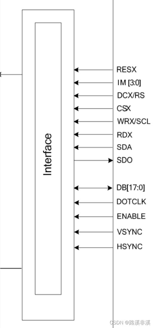
框图
以上注意,DCX/RS和WRX/SCL这两个引脚的功能是可配置的。
因此,具体厂家生产的液晶屏,需要核对好接口功能。
关键引脚
IM3 IM2 IM1 IM0这几位是决定使用哪种接口的。以及对应的一些位的作用。
复位
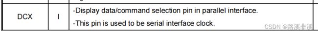
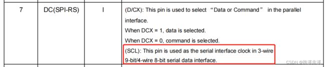
并行接口中用作数据/命令的选择位,SPI中用作时钟
片选,低电平使能
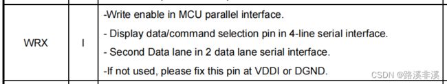
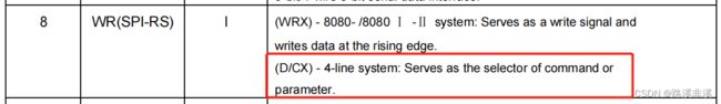
并口中是写使能,4线SPI中用作数据/命令选择接口
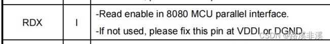
用在并口中,读使能
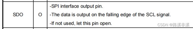
SPI接口的输入输出或者仅作为输入,数据在时钟的上升沿被锁存,要么是半双工,要么相当于MOSI引脚
SPI输出,在时钟下降沿输出数据,相当于MISO
DB[17:0] 并行口时用到的数据位。
注意,上面DCX/RS和WRX/SCL这两个引脚的RS和SCL功能,并未提及,不知道具体是什么含义。


针对具体的液晶屏ASL024HLCGB00-210
只实现了两种接口,IM3和IM0固定为0
当IM2和IM1均为1时,使用的就是4线8位SPI
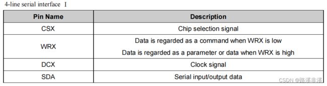
片选
时钟
IM3固化为低电平,因此是数据输入/输出口
这里只能实现半双工,其实,可以将SDA作为输入(上升沿),然后还有个单独的SDO作为输出(下降沿),以此实现全双工。
命令/参数选择


又回到ST7789V数据手册
直接关注四线八位SPI,4-line serial interface Ⅰ
引脚定义
片选
The write mode of the interface means the micro controller writes commands and data to the LCD driver.
In 4-lines serial interface, data packet contains just transmission byte and control bit WRX is transferred by the WRX pin. If WRX is “low”, the transmission byte is interpreted as a command byte. If WRX is “high”, the transmission byte is stored in the display data RAM (memory write command), or command register as parameter.
Any instruction can be sent in any order to the driver. The MSB is transmitted first. The serial interface is initialized when CSX is high. In this state, SCL clock pulse or SDA data have no effect. A falling edge on CSX enables the serial interface and indicates the start of data transmission.
写时序
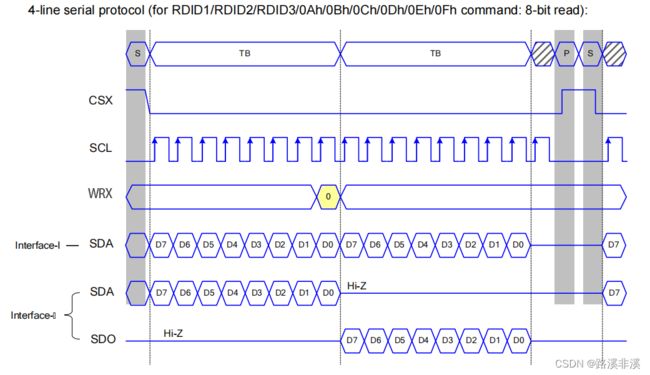
读时序
The read mode of the interface means that the micro controller reads register value from the driver. To achieve read function, the micro controller first has to send a command (read ID or register command) and then the following byte is transmitted in the opposite direction. After that CSX is required to go to high before a new command is send (see the below figure). The driver samples the SDA (input data) at rising edge of SCL, but shifts SDA (output data) at the falling edge of SCL. Thus the micro controller is supported to read at the
rising edge of SCL. After the read status command has been sent, the SDA line must be set to tri-state no later than at the falling edge of SCL of the last bit.
更多内容,详见数据手册。其他具体内容在实践中再总结补充吧。


相关命令参考数据手册9 COMMAND