FPGA—IIC 设计
FPGA—IIC 设计
串行同步半双工通信
特点
-
连接简单:只有两条总线(串行时钟总线SCL、串行数据总线SDA);
-
多主多从:可以有多个主机,多个从机;
-
ID唯一:由器件地址决定;
-
传输速度快:I2C 总线的传输速率标准模式下可以达到 100kb/s,快速模式下可以达到 400kb/s,高速模式下可达 3.4Mbit/s;
应用
数据量小,传输距离短,比如板级的通信
注意
在 I2C 总线的两根信号线 I2C_SCL 和 I2C_SDA 上都使用一个上拉电阻连接到了 3.3V 的电源上。该设计是为了适配各种不同的电平标准。I2C 总线上的所有器件的 SCL 和 SDC 引脚都是使用的开漏模式,本身是无法直接输出高电平的,需要通过外部的上拉电阻才能够支持,所以,在设计 I2C 总线应用电路时,该上拉电阻不能少。
IIC协议介绍
一次完整的传输包括 :起始位、停止位、控制字段、地址字段、读写数据字段
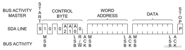
单字节地址写时序
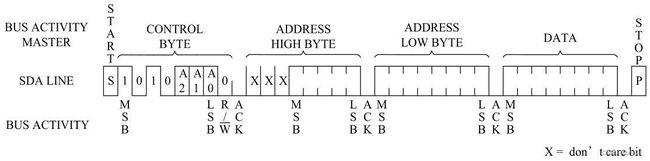
 #### 双字节地址写时序
单字节地址读时序
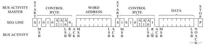
双字节地址读时序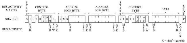
起始位
在时钟(SCL)为高电平的时候,数据总线(SDA)由高到低的跳变为总线 起始信号
停止位
在时钟(SCL)为高电平的时候,数据总线(SDA)由低到高的跳变为总线 停止信号
应答
应答,当数据发出方(不一定是主机还是从机)将 8 位数据或命令传出后,会将数据总线(SDA)释放,即设置为输入,然后等待数据接收方将 SDA 信号拉低以作为成功接收的应答信号。无论是什么状态,I2C 总线的 SCL 信号始终由 I2C 主机驱动。
RTL Code Design
代码参考了小梅哥的代码
1. 端口定义
module iic(
	clk,				//系统时钟
	rst_n,				//系统复位
	wr_en,				//写使能
	rd_en,				//读使能
	device_addr,		//器件地址
	reg_addr,			//寄存器地址
	reg_addr_num,		//寄存器地址字节数
	wr_data_num,  		//写数据字节数
	rd_data_num,  		//读数据
	sda,     			//IIC——SDA
	scl,				//IIC——SCL
	wr_data,			//写数据
	rd_data,			//读数据字节数
	wr_data_vaild,		//写数据有效
	rd_data_vaild,		//读数据有效
	done				//一次读写操作完成标志
);
/*端口定义*/
	input clk;					//系统时钟
	input rst_n;				//系统复位
	input wr_en;				//写使能
	input rd_en;				//读使能
	input [2:0]	 device_addr;	//器件地址
	input [15:0] reg_addr;		//寄存器地址
	input [1:0]	reg_addr_num;	//寄存器地址字节数
	input [5:0]	wr_data_num;  	//写数据字节数
	input [5:0]	rd_data_num;  	//读数据
	inout 		sda;     		//IIC——SDA
	output reg 	scl;			//IIC——SCL
    input 	   [7:0]wr_data;	//写数据
	output reg [7:0]rd_data;	//读数据字节数
	output 	   wr_data_vaild;	//读出数据有效
	output reg rd_data_vaild;	//写入数据有效
	output reg done;			//一次读写操作完成标志
2. 参数定义
	parameter SYS_CLOCK = 50_000_000;
	parameter SCL_CLOCK = 400_000;
	localparam SCL_CNT_M = SYS_CLOCK / SCL_CLOCK;
3. 状态定义
	localparam 	IDLE 		= 9'b0_0000_0001,
				WR_START 	= 9'b0_0000_0010,
				WR_CTRL 	= 9'b0_0000_0100,
				WR_REG_ADDR = 9'b0_0000_1000,
				WR_DATA 	= 9'b0_0001_0000,
				RD_START 	= 9'b0_0010_0000,
				RD_CTRL 	= 9'b0_0100_0000,
				RD_DATA 	= 9'b0_1000_0000,
				STOP 		= 9'b1_0000_0000;
4. 内部寄存器和信号定义
	reg  [8:0]main_state;	//状态寄存器
	reg sda_reg;			//sda输出寄存器
	reg sda_en;				//sda三态使能
	reg sda_task_flag;		//串行输出输入任务执行标志位
	reg w_flag;				//写标志
	reg r_flag;				//读标志
	reg  [15:0]scl_cnt;		//clk计数器,用于产生scl时钟
	reg scl_high;			//scl高电平中部标志
	reg scl_low;			//scl低电平中部标志
	reg scl_vaild;			//scl有效标志
	reg  [7:0]scl_level_cnt;//scl高低电平计数器
	reg ack;				//应答信号
	reg  [7:0]wdata_cnt;	//写数据字节数计数器
	reg  [7:0]rdata_cnt;	//读数据字节数计数器
	reg  [1:0]reg_addr_cnt;	//地址字节数计数器
	reg  [7:0]sda_data_out;	//数据输出buffer
	reg  [7:0]sda_data_in;	//数据输入buffer
	wire [7:0]wr_ctrl_word;	//写控制字
	wire [7:0]rd_ctrl_word;	//读控制字
	wire rdata_vaild_r; 	//读数据有效前寄存器
5. 读写控制字
	assign wr_ctrl_word = {4'b1010,device_addr,1'b0};
	assign rd_ctrl_word = {4'b1010,device_addr,1'b1};
6.scl 时钟输出
/* iic 非空闲状态产生 scl_vaild */
	always@(posedge clk or negedge rst_n)begin
		if(!rst_n)
			scl_vaild <= 1'b0;
		else if(wr_en | rd_en)
			scl_vaild <= 1'b1;
		else if(done)
			scl_vaild <= 1'b0;
		else
			scl_vaild <= scl_vaild;
	end

/* scl 计数器*/
	always@(posedge clk or negedge rst_n)begin
		if(!rst_n)
			scl_cnt <= 16'd0;
		else if(scl_vaild)begin
			if(scl_cnt==SCL_CNT_M-1)
				scl_cnt <= 16'd0;
			else
				scl_cnt <= scl_cnt + 16'd1;
		end
		else
			scl_cnt <= 16'd0;
	end

/* scl 时钟产生*/
	always@(posedge clk or negedge rst_n)begin
		if(!rst_n)
			scl <= 1'b1;
		else if(scl_cnt == SCL_CNT_M >> 1)
			scl <= 1'b0;
		else if(scl_cnt == 16'd0)
			scl <= 1'b1;
		else
			scl <= scl;
	end

/*scl 高低电平中部标志*/
	always@(posedge clk or negedge rst_n)begin
		if(!rst_n)
			scl_high <= 1'b0;
		else if(scl_cnt == (SCL_CNT_M >> 2))
			scl_high <= 1'b1;
		else
			scl_high <= 1'b0;
	end

	always@(posedge clk or negedge rst_n)begin
		if(!rst_n)
			scl_low <= 1'b0;
		else if(scl_cnt == ((SCL_CNT_M >> 1) + (SCL_CNT_M >> 2)))
			scl_low <= 1'b1;
		else
			scl_low <= 1'b0;
	end
7. 主状态机设计
	always@(posedge clk or negedge rst_n)begin
		if(!rst_n)begin
		//复位:空闲状态
				main_state 		<= IDLE;
				sda_reg 	  		<= 1'b1;
				w_flag 			<= 1'b0;
				r_flag 			<= 1'b0;
				done 				<= 1'b0;
				reg_addr_cnt 	<= 2'd1;
				wdata_cnt 		<= 8'd1;
				rdata_cnt 		<= 8'd1;
		end
		else begin
			case(main_state)
				IDLE:begin
					sda_reg   	 <= 1'b1;
					w_flag    	 <= 1'b0;
					r_flag 	 	 <= 1'b0;
					done 		    <= 1'b0;
					reg_addr_cnt <= 2'd1;
					wdata_cnt 	 <= 8'd1;
					rdata_cnt 	 <= 8'd1;
					if(wr_en)begin
						main_state <= WR_START;
						w_flag <= 1'b1;
					end
					else if(rd_en)begin
						main_state <= WR_START;
						r_flag <= 1'b1;
					end
					else
						main_state <= IDLE;
				end

				WR_START:begin
					if(scl_high)begin
						main_state <= WR_START;
						sda_reg <= 1'b0;
					end
					else if(scl_low)begin
						main_state <= WR_CTRL;
						sda_data_out <= wr_ctrl_word;	// 准备要发送的控制字
						sda_task_flag <= 1'b0; 			// 开始串行传输任务
					end
					else
					main_state <= WR_START;
				end
				WR_CTRL:begin
					if(sda_task_flag==1'b0)// 发送数据
						send_8bit_data;
					else begin	// 等待响应
						if(ack==1'b1)begin // 收到响应
							if(scl_low)begin// 准备发送的寄存器地址数据
								main_state 	  <= WR_REG_ADDR;// 转换到寄存器地址
								sda_task_flag <= 1'b0;
								if(reg_addr_num == 2'b1)
									sda_data_out <= reg_addr[7:0];
								else
									sda_data_out <= reg_addr[15:8];//如果寄存器地址为2个字节,要保证先发的最高位
							end
							else
								main_state <= WR_CTRL;
						end
						else // 未收到响应
							main_state <= IDLE;
					end
				end

				WR_REG_ADDR:begin
					if(sda_task_flag==1'b0)
						send_8bit_data;
					else begin
						if(ack==1'b1)begin //收到响应
							if(reg_addr_cnt == reg_addr_num)begin // 寄存器地址数据发送完成
								if(w_flag && scl_low)begin
									main_state    <= WR_DATA;//状态转移
									sda_data_out  <= wr_data;//数据准备
									sda_task_flag <= 1'b0;
									reg_addr_cnt  <= 2'd1;
								end
								else if(r_flag && scl_low)begin
									main_state <= RD_START;
									sda_reg <= 1'b1; //sda拉高
								end
								else
									main_state <= WR_REG_ADDR;
							end
							else begin									 // 寄存器地址数据没有发送完成
								if(scl_low)begin
									main_state <= WR_REG_ADDR;
									reg_addr_cnt <= reg_addr_cnt + 2'd1;
									sda_data_out <= reg_addr[7:0]; // 准备低8位寄存器地址
									sda_task_flag <= 1'b0;
								end
								else
									main_state <= WR_REG_ADDR;
							end
						end
						else	// 未收到响应
							main_state <= IDLE;

					end
				end

				WR_DATA:begin
					if(sda_task_flag==1'b0)
						send_8bit_data;
					else begin
						if(ack==1'b1)begin// 收到响应
							if(wdata_cnt == wr_data_num)begin //发送完成
								if(scl_low)begin
									main_state <= STOP;
									sda_reg 	  <= 1'b0;
									wdata_cnt  <= 8'd1;
								end
								else
									main_state <= WR_DATA;
							end
							else begin //未发送完成
								if(scl_low)begin
									main_state    <= WR_DATA;
									sda_data_out  <= wr_data;
									wdata_cnt     <= wdata_cnt + 8'd1;
									sda_task_flag <= 1'b0;
								end
								else
									main_state <= WR_DATA;
							end
						end
						else // 未收到响应
							main_state <= IDLE;
					end
				end

				RD_START:begin
					if(scl_high)begin
						main_state <= RD_START;
						sda_reg <= 1'b0;
					end
					else if(scl_low)begin
						main_state <= RD_CTRL;
						sda_data_out <= rd_ctrl_word;	// 准备要发送的控制字
						sda_task_flag <= 1'b0; 			// 开始串行传输任务
					end
					else
						main_state <= RD_START;
				end

				RD_CTRL:begin
					if(sda_task_flag==1'b0)// 发送数据
						send_8bit_data;
					else begin	// 等待响应
						if(ack==1'b1)begin // 收到响应
							if(scl_low)begin// 准备发送的寄存器地址数据
								main_state <= RD_DATA;// 转换到寄存器地址
								sda_task_flag <= 1'b0;
							end
							else
								main_state <= RD_CTRL;
						end
						else // 未收到响应
							main_state <= IDLE;
					end
				end

				RD_DATA:begin
					if(sda_task_flag==1'b0)begin
						receive_8bit_data;
					end
					else begin
						if(rdata_cnt==rd_data_num)begin// 接收完成
							sda_reg <= 1'b1; //发送 ACK,不读了
							if(scl_low)begin
								main_state <= STOP;
								sda_reg <= 1'b0;
							end
							else
								main_state <= RD_DATA;
						end
						else begin
							sda_reg <= 1'b0; // 发送NACK,继续读下一个字节
							if(scl_low)begin
								main_state <= RD_DATA;
								rdata_cnt <= rdata_cnt + 8'd1;
								sda_task_flag <= 1'b0;
							end
							else
								main_state <= RD_DATA;
						end
					end
				end

				STOP:begin
					if(scl_high)begin
						sda_reg    <= 1'b1;
						main_state <= IDLE;
						done       <= 1'b1;
					end
					else
						main_state <= STOP;
				end

				default:main_state <= IDLE;
			endcase
		end

	end
8. 发送接收任务
/* 发送接收8bit数据任务*/
	/*发送接收数据时 scl 时钟计数*/
	always@(posedge clk or negedge rst_n)begin
		if(!rst_n)
			scl_level_cnt <= 8'd0;
        else if(main_state == WR_CTRL || main_state == WR_REG_ADDR || main_state == WR_DATA ||
				main_state == RD_CTRL || main_state == RD_DATA)begin //只有这几个状态需要执行数据发送接收任务
			if(scl_low | scl_high)begin
				if(scl_level_cnt == 8'd17)
					scl_level_cnt <= 8'd0;
				else
					scl_level_cnt <= scl_level_cnt + 8'd1;
			end
			else
				scl_level_cnt <= scl_level_cnt;
		end
		else
			scl_level_cnt <= 8'd0;
	end


	/*数据接收对发送的响应标志位*/
	always@(posedge clk or negedge rst_n)begin
		if(!rst_n)
			ack <= 1'b0;
		else if(scl_level_cnt == 8'd16 && scl_high && sda===1'd0)
			ack <= 1'b1;
		else if((scl_level_cnt == 8'd17)&& scl_low)
			ack <= 1'b0;
		else
			ack <= ack;
	end

	/* 输出串行数据任务 */
	// scl_high &
	task send_8bit_data;
		if(scl_high && (scl_level_cnt == 8'd16))//8bit data send done
			sda_task_flag <= 1'b1;
		else if(scl_level_cnt < 8'd17)begin
			sda_reg <= sda_data_out[7];
			if(scl_low)
				sda_data_out <= {sda_data_out[6:0],1'b0};
			else
				sda_data_out <= sda_data_out;
		end
		else
			;
	endtask

	/* 接收串行数据任务 */
	// scl_high & scl_level_cnt==15 接收完成
	// scl_low  & scl_level_cnt==15 退出任务
	task receive_8bit_data;
		if(scl_low && (scl_level_cnt==8'd15))
			sda_task_flag <= 1'b1;
		else if(scl_level_cnt < 8'd15)begin
			if(scl_high)
				sda_data_in <= {sda_data_in[6:0],sda};
			else
				sda_data_in <= sda_data_in;
		end
		else
			;
	endtask
9. sda 三态门输出控制
	/*sda 三态门输出*/
	assign sda = sda_en ? sda_reg : 1'bz;

	always@(*)begin
		case(main_state)
			IDLE:
				sda_en <= 1'b0;//输入

			WR_START,RD_START,STOP :
				sda_en <= 1'b1;//输出

			WR_CTRL,WR_REG_ADDR,WR_DATA,RD_CTRL:
				if(scl_level_cnt < 16)
					sda_en <= 1'b1;
				else
					sda_en <= 1'b0;

			RD_DATA:
				if(scl_level_cnt < 16)
					sda_en <= 1'b0;
				else
					sda_en <= 1'b1;
			default:
					sda_en <= 1'b0;
		endcase
	end
10.读&写数据有效标志位
	assign wr_data_vaild = ((main_state==WR_REG_ADDR)&&
	                        (reg_addr_cnt==reg_addr_num)&&
						 	(w_flag && scl_low)&&
							(ack == 1'b1))||
                     	   ((main_state == WR_DATA)&&
							(ack == 1'b1)&&
                            (scl_low)&&
							(wdata_cnt != wr_data_num));
	/*读出数据有效标志位*/
	assign rdata_vaild_r = (main_state==RD_DATA) && (scl_level_cnt == 8'd15) && scl_low;
	always@(posedge clk or negedge rst_n)begin
		if(!rst_n)
			rd_data_vaild <= 1'b0;
		else if(rdata_vaild_r)
			rd_data_vaild <= 1'b1;
		else
			rd_data_vaild <= 1'b0;
	end
11. 读出有效数据
	/*读出的有效数据*/
	always@(posedge clk or negedge rst_n)begin
		if(!rst_n)
			rd_data <= 8'd0;
		else if(rdata_vaild_r)
			rd_data <= sda_data_in;
		else
			rd_data <= rd_data;
	end
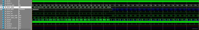
12.仿真波形
24LC64.v
// *******************************************************************************************************
// ** **
// ** 24LC64.v - Microchip 24LC64 64K-BIT I2C SERIAL EEPROM (VCC = +2.5V TO +5.5V) **
// ** **
// *******************************************************************************************************
// ** **
// ** This information is distributed under license from Young Engineering. **
// ** COPYRIGHT (c) 2009 YOUNG ENGINEERING **
// ** ALL RIGHTS RESERVED **
// ** **
// ** **
// ** Young Engineering provides design expertise for the digital world **
// ** Started in 1990, Young Engineering offers products and services for your electronic design **
// ** project. We have the expertise in PCB, FPGA, ASIC, firmware, and software design. **
// ** From concept to prototype to production, we can help you. **
// ** **
// ** http://www.young-engineering.com/ **
// ** **
// *******************************************************************************************************
// ** This information is provided to you for your convenience and use with Microchip products only. **
// ** Microchip disclaims all liability arising from this information and its use. **
// ** **
// ** THIS INFORMATION IS PROVIDED "AS IS." MICROCHIP MAKES NO REPRESENTATION OR WARRANTIES OF **
// ** ANY KIND WHETHER EXPRESS OR IMPLIED, WRITTEN OR ORAL, STATUTORY OR OTHERWISE, RELATED TO **
// ** THE INFORMATION PROVIDED TO YOU, INCLUDING BUT NOT LIMITED TO ITS CONDITION, QUALITY, **
// ** PERFORMANCE, MERCHANTABILITY, NON-INFRINGEMENT, OR FITNESS FOR PURPOSE. **
// ** MICROCHIP IS NOT LIABLE, UNDER ANY CIRCUMSTANCES, FOR SPECIAL, INCIDENTAL OR CONSEQUENTIAL **
// ** DAMAGES, FOR ANY REASON WHATSOEVER. **
// ** **
// ** It is your responsibility to ensure that your application meets with your specifications. **
// ** **
// *******************************************************************************************************
// ** Revision : 1.4 **
// ** Modified Date : 02/04/2009 **
// ** Revision History: **
// ** **
// ** 10/01/2003: Initial design **
// ** 07/19/2004: Fixed the timing checks and the open-drain modeling for SDA. **
// ** 01/06/2006: Changed the legal information in the header **
// ** 12/04/2006: Corrected timing checks to reference proper clock edges **
// ** Added timing check for Tbuf (bus free time) **
// ** Reduced memory blocks to single, monolithic array **
// ** 02/04/2009: Added timing checks for tSU_WP and tHD_WP **
// ** **
// *******************************************************************************************************
// ** TABLE OF CONTENTS **
// *******************************************************************************************************
// **---------------------------------------------------------------------------------------------------**
// ** DECLARATIONS **
// **---------------------------------------------------------------------------------------------------**
// **---------------------------------------------------------------------------------------------------**
// ** INITIALIZATION **
// **---------------------------------------------------------------------------------------------------**
// **---------------------------------------------------------------------------------------------------**
// ** CORE LOGIC **
// **---------------------------------------------------------------------------------------------------**
// ** 1.01: START Bit Detection **
// ** 1.02: STOP Bit Detection **
// ** 1.03: Input Shift Register **
// ** 1.04: Input Bit Counter **
// ** 1.05: Control Byte Register **
// ** 1.06: Byte Address Register **
// ** 1.07: Write Data Buffer **
// ** 1.08: Acknowledge Generator **
// ** 1.09: Acknowledge Detect **
// ** 1.10: Write Cycle Timer **
// ** 1.11: Write Cycle Processor **
// ** 1.12: Read Data Multiplexor **
// ** 1.13: Read Data Processor **
// ** 1.14: SDA Data I/O Buffer **
// ** **
// **---------------------------------------------------------------------------------------------------**
// ** DEBUG LOGIC **
// **---------------------------------------------------------------------------------------------------**
// ** 2.01: Memory Data Bytes **
// ** 2.02: Write Data Buffer **
// ** **
// **---------------------------------------------------------------------------------------------------**
// ** TIMING CHECKS **
// **---------------------------------------------------------------------------------------------------**
// ** **
// *******************************************************************************************************
`timescale 1ns/10ps
module M24LC64 (A0, A1, A2, WP, SDA, SCL, RESET);
input A0; // chip select bit
input A1; // chip select bit
input A2; // chip select bit
input WP; // write protect pin
inout SDA; // serial data I/O
input SCL; // serial data clock
input RESET; // system reset
// *******************************************************************************************************
// ** DECLARATIONS **
// *******************************************************************************************************
reg SDA_DO; // serial data - output
reg SDA_OE; // serial data - output enable
wire SDA_DriveEnable; // serial data output enable
reg SDA_DriveEnableDlyd; // serial data output enable - delayed
wire [02:00] ChipAddress; // hardwired chip address
reg [03:00] BitCounter; // serial bit counter
reg START_Rcvd; // START bit received flag
reg STOP_Rcvd; // STOP bit received flag
reg CTRL_Rcvd; // control byte received flag
reg ADHI_Rcvd; // byte address hi received flag
reg ADLO_Rcvd; // byte address lo received flag
reg MACK_Rcvd; // master acknowledge received flag
reg WrCycle; // memory write cycle
reg RdCycle; // memory read cycle
reg [07:00] ShiftRegister; // input data shift register
reg [07:00] ControlByte; // control byte register
wire RdWrBit; // read/write control bit
reg [12:00] StartAddress; // memory access starting address
reg [04:00] PageAddress; // memory page address
reg [07:00] WrDataByte [0:31]; // memory write data buffer
wire [07:00] RdDataByte; // memory read data
reg [15:00] WrCounter; // write buffer counter
reg [04:00] WrPointer; // write buffer pointer
reg [12:00] RdPointer; // read address pointer
reg WriteActive; // memory write cycle active
reg [07:00] MemoryBlock [0:8191]; // EEPROM data memory array
integer LoopIndex; // iterative loop index
integer tAA; // timing parameter
integer tWC; // timing parameter
// *******************************************************************************************************
// ** INITIALIZATION **
// *******************************************************************************************************
//----------------------------
//------写数据间隔改动----------
initial tAA = 900; // SCL to SDA output delay
initial tWC = 500; // memory write cycle time
// initial tAA = 900; // SCL to SDA output delay
// initial tWC = 5000000; // memory write cycle time
initial begin
SDA_DO = 0;
SDA_OE = 0;
end
initial begin
START_Rcvd = 0;
STOP_Rcvd = 0;
CTRL_Rcvd = 0;
ADHI_Rcvd = 0;
ADLO_Rcvd = 0;
MACK_Rcvd = 0;
end
initial begin
BitCounter = 0;
ControlByte = 0;
end
initial begin
WrCycle = 0;
RdCycle = 0;
WriteActive = 0;
end
assign ChipAddress = {A2,A1,A0};
// *******************************************************************************************************
// ** CORE LOGIC **
// *******************************************************************************************************
// -------------------------------------------------------------------------------------------------------
// 1.01: START Bit Detection
// -------------------------------------------------------------------------------------------------------
always @(negedge SDA) begin
if (SCL == 1) begin
START_Rcvd <= 1;
STOP_Rcvd <= 0;
CTRL_Rcvd <= 0;
ADHI_Rcvd <= 0;
ADLO_Rcvd <= 0;
MACK_Rcvd <= 0;
WrCycle <= #1 0;
RdCycle <= #1 0;
BitCounter <= 0;
end
end
// -------------------------------------------------------------------------------------------------------
// 1.02: STOP Bit Detection
// -------------------------------------------------------------------------------------------------------
always @(posedge SDA) begin
if (SCL == 1) begin
START_Rcvd <= 0;
STOP_Rcvd <= 1;
CTRL_Rcvd <= 0;
ADHI_Rcvd <= 0;
ADLO_Rcvd <= 0;
MACK_Rcvd <= 0;
WrCycle <= #1 0;
RdCycle <= #1 0;
BitCounter <= 10;
end
end
// -------------------------------------------------------------------------------------------------------
// 1.03: Input Shift Register
// -------------------------------------------------------------------------------------------------------
always @(posedge SCL) begin
ShiftRegister[00] <= SDA;
ShiftRegister[01] <= ShiftRegister[00];
ShiftRegister[02] <= ShiftRegister[01];
ShiftRegister[03] <= ShiftRegister[02];
ShiftRegister[04] <= ShiftRegister[03];
ShiftRegister[05] <= ShiftRegister[04];
ShiftRegister[06] <= ShiftRegister[05];
ShiftRegister[07] <= ShiftRegister[06];
end
// -------------------------------------------------------------------------------------------------------
// 1.04: Input Bit Counter
// -------------------------------------------------------------------------------------------------------
always @(posedge SCL) begin
if (BitCounter < 10) BitCounter <= BitCounter + 1;
end
// -------------------------------------------------------------------------------------------------------
// 1.05: Control Byte Register
// -------------------------------------------------------------------------------------------------------
always @(negedge SCL) begin
if (START_Rcvd & (BitCounter == 8)) begin
if (!WriteActive & (ShiftRegister[07:01] == {4'b1010,ChipAddress[02:00]})) begin
if (ShiftRegister[00] == 0) WrCycle <= 1;
if (ShiftRegister[00] == 1) RdCycle <= 1;
ControlByte <= ShiftRegister[07:00];
CTRL_Rcvd <= 1;
end
START_Rcvd <= 0;
end
end
assign RdWrBit = ControlByte[00];
// -------------------------------------------------------------------------------------------------------
// 1.06: Byte Address Register
// -------------------------------------------------------------------------------------------------------
always @(negedge SCL) begin
if (CTRL_Rcvd & (BitCounter == 8)) begin
if (RdWrBit == 0) begin
StartAddress[12:08] <= ShiftRegister[04:00];
RdPointer[12:08] <= ShiftRegister[04:00];
ADHI_Rcvd <= 1;
end
WrCounter <= 0;
WrPointer <= 0;
CTRL_Rcvd <= 0;
end
end
always @(negedge SCL) begin
if (ADHI_Rcvd & (BitCounter == 8)) begin
if (RdWrBit == 0) begin
StartAddress[07:00] <= ShiftRegister[07:00];
RdPointer[07:00] <= ShiftRegister[07:00];
ADLO_Rcvd <= 1;
end
WrCounter <= 0;
WrPointer <= 0;
ADHI_Rcvd <= 0;
end
end
// -------------------------------------------------------------------------------------------------------
// 1.07: Write Data Buffer
// -------------------------------------------------------------------------------------------------------
always @(negedge SCL) begin
if (ADLO_Rcvd & (BitCounter == 8)) begin
if (RdWrBit == 0) begin
WrDataByte[WrPointer] <= ShiftRegister[07:00];
WrCounter <= WrCounter + 1;
WrPointer <= WrPointer + 1;
end
end
end
// -------------------------------------------------------------------------------------------------------
// 1.08: Acknowledge Generator
// -------------------------------------------------------------------------------------------------------
always @(negedge SCL) begin
if (!WriteActive) begin
if (BitCounter == 8) begin
if (WrCycle | (START_Rcvd & (ShiftRegister[07:01] == {4'b1010,ChipAddress[02:00]}))) begin
SDA_DO <= 0;
SDA_OE <= 1;
end
end
if (BitCounter == 9) begin
BitCounter <= 0;
if (!RdCycle) begin
SDA_DO <= 0;
SDA_OE <= 0;
end
end
end
end
// -------------------------------------------------------------------------------------------------------
// 1.09: Acknowledge Detect
// -------------------------------------------------------------------------------------------------------
always @(posedge SCL) begin
if (RdCycle & (BitCounter == 8)) begin
if ((SDA == 0) & (SDA_OE == 0)) MACK_Rcvd <= 1;
end
end
always @(negedge SCL) MACK_Rcvd <= 0;
// -------------------------------------------------------------------------------------------------------
// 1.10: Write Cycle Timer
// -------------------------------------------------------------------------------------------------------
always @(posedge STOP_Rcvd) begin
if (WrCycle & (WP == 0) & (WrCounter > 0)) begin
WriteActive = 1;
#(tWC);
WriteActive = 0;
end
end
always @(posedge STOP_Rcvd) begin
#(1.0);
STOP_Rcvd = 0;
end
// -------------------------------------------------------------------------------------------------------
// 1.11: Write Cycle Processor
// -------------------------------------------------------------------------------------------------------
always @(negedge WriteActive) begin
for (LoopIndex = 0; LoopIndex < WrCounter; LoopIndex = LoopIndex + 1) begin
PageAddress = StartAddress[04:00] + LoopIndex;
MemoryBlock[{StartAddress[12:05],PageAddress[04:00]}] = WrDataByte[LoopIndex[04:00]];
end
end
// -------------------------------------------------------------------------------------------------------
// 1.12: Read Data Multiplexor
// -------------------------------------------------------------------------------------------------------
always @(negedge SCL) begin
if (BitCounter == 8) begin
if (WrCycle & ADLO_Rcvd) begin
RdPointer <= StartAddress + WrPointer + 1;
end
if (RdCycle) begin
RdPointer <= RdPointer + 1;
end
end
end
assign RdDataByte = MemoryBlock[RdPointer[12:00]];
// -------------------------------------------------------------------------------------------------------
// 1.13: Read Data Processor
// -------------------------------------------------------------------------------------------------------
always @(negedge SCL) begin
if (RdCycle) begin
if (BitCounter == 8) begin
SDA_DO <= 0;
SDA_OE <= 0;
end
else if (BitCounter == 9) begin
SDA_DO <= RdDataByte[07];
if (MACK_Rcvd) SDA_OE <= 1;
end
else begin
SDA_DO <= RdDataByte[7-BitCounter];
end
end
end
// -------------------------------------------------------------------------------------------------------
// 1.14: SDA Data I/O Buffer
// -------------------------------------------------------------------------------------------------------
bufif1 (SDA, 1'b0, SDA_DriveEnableDlyd);
assign SDA_DriveEnable = !SDA_DO & SDA_OE;
always @(SDA_DriveEnable) SDA_DriveEnableDlyd <= #(tAA) SDA_DriveEnable;
// *******************************************************************************************************
// ** DEBUG LOGIC **
// *******************************************************************************************************
// -------------------------------------------------------------------------------------------------------
// 2.01: Memory Data Bytes
// -------------------------------------------------------------------------------------------------------
wire [07:00] MemoryByte_000 = MemoryBlock[00];
wire [07:00] MemoryByte_001 = MemoryBlock[01];
wire [07:00] MemoryByte_002 = MemoryBlock[02];
wire [07:00] MemoryByte_003 = MemoryBlock[03];
wire [07:00] MemoryByte_004 = MemoryBlock[04];
wire [07:00] MemoryByte_005 = MemoryBlock[05];
wire [07:00] MemoryByte_006 = MemoryBlock[06];
wire [07:00] MemoryByte_007 = MemoryBlock[07];
wire [07:00] MemoryByte_008 = MemoryBlock[08];
wire [07:00] MemoryByte_009 = MemoryBlock[09];
wire [07:00] MemoryByte_00A = MemoryBlock[10];
wire [07:00] MemoryByte_00B = MemoryBlock[11];
wire [07:00] MemoryByte_00C = MemoryBlock[12];
wire [07:00] MemoryByte_00D = MemoryBlock[13];
wire [07:00] MemoryByte_00E = MemoryBlock[14];
wire [07:00] MemoryByte_00F = MemoryBlock[15];
// -------------------------------------------------------------------------------------------------------
// 2.02: Write Data Buffer
// -------------------------------------------------------------------------------------------------------
wire [07:00] WriteData_00 = WrDataByte[00];
wire [07:00] WriteData_01 = WrDataByte[01];
wire [07:00] WriteData_02 = WrDataByte[02];
wire [07:00] WriteData_03 = WrDataByte[03];
wire [07:00] WriteData_04 = WrDataByte[04];
wire [07:00] WriteData_05 = WrDataByte[05];
wire [07:00] WriteData_06 = WrDataByte[06];
wire [07:00] WriteData_07 = WrDataByte[07];
wire [07:00] WriteData_08 = WrDataByte[08];
wire [07:00] WriteData_09 = WrDataByte[09];
wire [07:00] WriteData_0A = WrDataByte[10];
wire [07:00] WriteData_0B = WrDataByte[11];
wire [07:00] WriteData_0C = WrDataByte[12];
wire [07:00] WriteData_0D = WrDataByte[13];
wire [07:00] WriteData_0E = WrDataByte[14];
wire [07:00] WriteData_0F = WrDataByte[15];
wire [07:00] WriteData_10 = WrDataByte[16];
wire [07:00] WriteData_11 = WrDataByte[17];
wire [07:00] WriteData_12 = WrDataByte[18];
wire [07:00] WriteData_13 = WrDataByte[19];
wire [07:00] WriteData_14 = WrDataByte[20];
wire [07:00] WriteData_15 = WrDataByte[21];
wire [07:00] WriteData_16 = WrDataByte[22];
wire [07:00] WriteData_17 = WrDataByte[23];
wire [07:00] WriteData_18 = WrDataByte[24];
wire [07:00] WriteData_19 = WrDataByte[25];
wire [07:00] WriteData_1A = WrDataByte[26];
wire [07:00] WriteData_1B = WrDataByte[27];
wire [07:00] WriteData_1C = WrDataByte[28];
wire [07:00] WriteData_1D = WrDataByte[29];
wire [07:00] WriteData_1E = WrDataByte[30];
wire [07:00] WriteData_1F = WrDataByte[31];
// *******************************************************************************************************
// ** TIMING CHECKS **
// *******************************************************************************************************
wire TimingCheckEnable = (RESET == 0) & (SDA_OE == 0);
wire StopTimingCheckEnable = TimingCheckEnable && SCL;
//--------------------------------
//-------仿真时时序约束需改动--------
//--------------------------------
specify
specparam
tHI = 600, // SCL pulse width - high
// tLO = 1300, // SCL pulse width - low
tLO = 600,
tSU_STA = 600, // SCL to SDA setup time
tHD_STA = 600, // SCL to SDA hold time
tSU_DAT = 100, // SDA to SCL setup time
tSU_STO = 600, // SCL to SDA setup time
tSU_WP = 600, // WP to SDA setup time
tHD_WP = 1300, // WP to SDA hold time
// tBUF = 1300; // Bus free time
tBUF = 600;
$width (posedge SCL, tHI);
$width (negedge SCL, tLO);
$width (posedge SDA &&& SCL, tBUF);
$setup (posedge SCL, negedge SDA &&& TimingCheckEnable, tSU_STA);
$setup (SDA, posedge SCL &&& TimingCheckEnable, tSU_DAT);
$setup (posedge SCL, posedge SDA &&& TimingCheckEnable, tSU_STO);
$setup (WP, posedge SDA &&& StopTimingCheckEnable, tSU_WP);
$hold (negedge SDA &&& TimingCheckEnable, negedge SCL, tHD_STA);
$hold (posedge SDA &&& StopTimingCheckEnable, WP, tHD_WP);
endspecify
endmodule
24LC04B.v
// *******************************************************************************************************
// **                                                                           			**
// **   24LC04B.v - Microchip 24LC04B 4K-BIT I2C SERIAL EEPROM (VCC = +2.5V TO +5.5V)			**
// **                                                                           			**
// *******************************************************************************************************
// **                                                                           			**
// **			This information is distributed under license from Young Engineering.		**
// **                              COPYRIGHT (c) 2003 YOUNG ENGINEERING              			**
// **                                      ALL RIGHTS RESERVED                         			**
// **                                                                           			**
// **                                                                                                   **
// **   Young Engineering provides design expertise for the digital world                               **
// **   Started in 1990, Young Engineering offers products and services for your electronic design      **
// **   project.  We have the expertise in PCB, FPGA, ASIC, firmware, and software design.              **
// **   From concept to prototype to production, we can help you.                                       **
// **													**
// **	http://www.young-engineering.com/								**
// **													**
// *******************************************************************************************************
// **	This information is provided to you for your convenience and use with Microchip products only.  **
// **	Microchip disclaims all liability arising from this information and its use.  			**
// **													**
// **	THIS INFORMATION IS PROVIDED "AS IS." MICROCHIP MAKES NO REPRESENTATION OR WARRANTIES OF 	**
// **	ANY KIND WHETHER EXPRESS OR IMPLIED, WRITTEN OR ORAL, STATUTORY OR OTHERWISE, RELATED TO 	**
// **	THE INFORMATION PROVIDED TO YOU, INCLUDING BUT NOT LIMITED TO ITS CONDITION, QUALITY, 		**
// **	PERFORMANCE, MERCHANTABILITY, NON-INFRINGEMENT, OR FITNESS FOR PURPOSE.  			**
// **	MICROCHIP IS NOT LIABLE, UNDER ANY CIRCUMSTANCES, FOR SPECIAL, INCIDENTAL OR CONSEQUENTIAL 	**
// **	DAMAGES, FOR ANY REASON WHATSOEVER.								**
// **													**
// **	It is your responsibility to ensure that your application meets with your specifications.	**
// **													**
// *******************************************************************************************************
// **   Revision       : 1.3                                                    			**
// **   Modified Date  : 12/04/2006	                                            			**
// **   Revision History:                                                       			**
// **                                                                           			**
// **   02/01/2003:  Initial design                                             			**
// **   07/19/2004:  Fixed the timing checks and the open-drain modeling for SDA.			**
// **   01/06/2006:  Changed the legal information in the header					**
// **   12/04/2006:  Corrected timing checks to reference proper clock edges				**
// **                Added timing check for Tbuf (bus free time)					**
// **                                                                           			**
// *******************************************************************************************************
// **                                       TABLE OF CONTENTS                          			**
// *******************************************************************************************************
// **---------------------------------------------------------------------------------------------------**
// **   DECLARATIONS                                                          				**
// **---------------------------------------------------------------------------------------------------**
// **---------------------------------------------------------------------------------------------------**
// **   INITIALIZATION                                              					**
// **---------------------------------------------------------------------------------------------------**
// **---------------------------------------------------------------------------------------------------**
// **   CORE LOGIC                                                  					**
// **---------------------------------------------------------------------------------------------------**
// **   1.01:  START Bit Detection									**
// **   1.02:  STOP Bit Detection									**
// **   1.03:  Input Shift Register									**
// **   1.04:  Input Bit Counter									**
// **   1.05:  Control Byte Register									**
// **   1.06:  Byte Address Register									**
// **   1.07:  Write Data Buffer									**
// **   1.08:  Acknowledge Generator									**
// **   1.09:  Acknowledge Detect									**
// **   1.10:  Write Cycle Timer									**
// **   1.11:  Write Cycle Processor									**
// **   1.12:  Read Data Multiplexor									**
// **   1.13:  Read Data Processor									**
// **   1.14:  SDA Data I/O Buffer									**
// **                                                                           			**
// **---------------------------------------------------------------------------------------------------**
// **   DEBUG LOGIC                                                  					**
// **---------------------------------------------------------------------------------------------------**
// **   2.01:  Memory Data Bytes									**
// **   2.02:  Write Data Buffer									**
// **                                                                           			**
// **---------------------------------------------------------------------------------------------------**
// **   TIMING CHECKS                                                     				**
// **---------------------------------------------------------------------------------------------------**
// **                                                                           			**
// *******************************************************************************************************


`timescale 1ns/10ps

module M24LC04B (A0, A1, A2, WP, SDA, SCL, RESET);

   input 		A0;				// unconnected pin
   input 		A1;				// unconnected pin
   input 		A2;				// unconnected pin

   input		WP;				// write protect pin

   inout		SDA;				// serial data I/O
   input		SCL;				// serial data clock

   input		RESET;				// system reset


// *******************************************************************************************************
// **   DECLARATIONS                                                            			**
// *******************************************************************************************************

   reg			SDA_DO;				// serial data - output
   reg			SDA_OE;				// serial data - output enable

   wire			SDA_DriveEnable;		// serial data output enable
   reg			SDA_DriveEnableDlyd;		// serial data output enable - delayed

   reg	[03:00]		BitCounter;			// serial bit counter

   reg			START_Rcvd;			// START bit received flag
   reg			STOP_Rcvd;			// STOP bit received flag
   reg			CTRL_Rcvd;			// control byte received flag
   reg			ADDR_Rcvd;			// byte address received flag
   reg			MACK_Rcvd;			// master acknowledge received flag

   reg			WrCycle;			// memory write cycle
   reg			RdCycle;			// memory read cycle

   reg	[07:00]		ShiftRegister;			// input data shift register

   reg  [07:00]		ControlByte;			// control byte register
   wire			BlockSelect;			// memory block select
   wire			RdWrBit;			// read/write control bit

   reg	[08:00]		StartAddress;			// memory access starting address
   reg	[03:00]		PageAddress;			// memory page address

   reg	[07:00]		WrDataByte [0:15];		// memory write data buffer
   wire	[07:00]		RdDataByte;			// memory read data

   reg	[15:00]		WrCounter;			// write buffer counter

   reg	[03:00]		WrPointer;			// write buffer pointer
   reg	[08:00]		RdPointer;			// read address pointer

   reg			WriteActive;			// memory write cycle active

   reg	[07:00]		MemoryBlock0 [0:255];		// EEPROM data memory array
   reg	[07:00]		MemoryBlock1 [0:255];		// EEPROM data memory array

   integer		LoopIndex;			// iterative loop index

   integer 		tAA;				// timing parameter
   integer 		tWC;				// timing parameter


// *******************************************************************************************************
// **   INITIALIZATION                                                         				**
// *******************************************************************************************************

//----------------------------
//------写数据间隔改动----------
   initial tAA = 900;                                   // SCL to SDA output delay
   initial tWC = 500;                                   // memory write cycle time

//   initial tAA = 900;					// SCL to SDA output delay
//   initial tWC = 5000000;				// memory write cycle time

   initial begin
      SDA_DO = 0;
      SDA_OE = 0;
   end

   initial begin
      START_Rcvd = 0;
      STOP_Rcvd  = 0;
      CTRL_Rcvd  = 0;
      ADDR_Rcvd  = 0;
      MACK_Rcvd  = 0;
   end

   initial begin
      BitCounter  = 0;
      ControlByte = 0;
   end

   initial begin
      WrCycle = 0;
      RdCycle = 0;

      WriteActive = 0;
   end


// *******************************************************************************************************
// **   CORE LOGIC                                                    					**
// *******************************************************************************************************
// -------------------------------------------------------------------------------------------------------
//      1.01:  START Bit Detection
// -------------------------------------------------------------------------------------------------------

   always @(negedge SDA) begin
      if (SCL == 1) begin
         START_Rcvd <= 1;
         STOP_Rcvd  <= 0;
         CTRL_Rcvd  <= 0;
         ADDR_Rcvd  <= 0;
         MACK_Rcvd  <= 0;

         WrCycle <= #1 0;
         RdCycle <= #1 0;

         BitCounter <= 0;
      end
   end

// -------------------------------------------------------------------------------------------------------
//      1.02:  STOP Bit Detection
// -------------------------------------------------------------------------------------------------------

   always @(posedge SDA) begin
      if (SCL == 1) begin
         START_Rcvd <= 0;
         STOP_Rcvd  <= 1;
         CTRL_Rcvd  <= 0;
         ADDR_Rcvd  <= 0;
         MACK_Rcvd  <= 0;

         WrCycle <= #1 0;
         RdCycle <= #1 0;

         BitCounter <= 10;
      end
   end

// -------------------------------------------------------------------------------------------------------
//      1.03:  Input Shift Register
// -------------------------------------------------------------------------------------------------------

   always @(posedge SCL) begin
      ShiftRegister[00] <= SDA;
      ShiftRegister[01] <= ShiftRegister[00];
      ShiftRegister[02] <= ShiftRegister[01];
      ShiftRegister[03] <= ShiftRegister[02];
      ShiftRegister[04] <= ShiftRegister[03];
      ShiftRegister[05] <= ShiftRegister[04];
      ShiftRegister[06] <= ShiftRegister[05];
      ShiftRegister[07] <= ShiftRegister[06];
   end

// -------------------------------------------------------------------------------------------------------
//      1.04:  Input Bit Counter
// -------------------------------------------------------------------------------------------------------

   always @(posedge SCL) begin
      if (BitCounter < 10) BitCounter <= BitCounter + 1;
   end

// -------------------------------------------------------------------------------------------------------
//      1.05:  Control Byte Register
// -------------------------------------------------------------------------------------------------------

   always @(negedge SCL) begin
      if (START_Rcvd & (BitCounter == 8)) begin
         if (!WriteActive & (ShiftRegister[07:04] == 4'b1010)) begin
            if (ShiftRegister[00] == 0) WrCycle <= 1;
            if (ShiftRegister[00] == 1) RdCycle <= 1;

            ControlByte <= ShiftRegister[07:00];

            CTRL_Rcvd <= 1;
         end

         START_Rcvd <= 0;
      end
   end

   assign BlockSelect = ControlByte[01];
   assign RdWrBit     = ControlByte[00];

// -------------------------------------------------------------------------------------------------------
//      1.06:  Byte Address Register
// -------------------------------------------------------------------------------------------------------

   always @(negedge SCL) begin
      if (CTRL_Rcvd & (BitCounter == 8)) begin
         if (RdWrBit == 0) begin
            StartAddress <= {BlockSelect,ShiftRegister[07:00]};
            RdPointer    <= {BlockSelect,ShiftRegister[07:00]};

            ADDR_Rcvd <= 1;
         end

         WrCounter <= 0;
         WrPointer <= 0;

         CTRL_Rcvd <= 0;
      end
   end

// -------------------------------------------------------------------------------------------------------
//      1.07:  Write Data Buffer
// -------------------------------------------------------------------------------------------------------

   always @(negedge SCL) begin
      if (ADDR_Rcvd & (BitCounter == 8)) begin
         if ((WP == 0) & (RdWrBit == 0)) begin
            WrDataByte[WrPointer] <= ShiftRegister[07:00];

            WrCounter <= WrCounter + 1;
            WrPointer <= WrPointer + 1;
         end
      end
   end

// -------------------------------------------------------------------------------------------------------
//      1.08:  Acknowledge Generator
// -------------------------------------------------------------------------------------------------------

   always @(negedge SCL) begin
      if (!WriteActive) begin
         if (BitCounter == 8) begin
            if (WrCycle | (START_Rcvd & (ShiftRegister[07:04] == 4'b1010))) begin
               SDA_DO <= 0;
               SDA_OE <= 1;
            end
         end
         if (BitCounter == 9) begin
            BitCounter <= 0;

            if (!RdCycle) begin
               SDA_DO <= 0;
               SDA_OE <= 0;
            end
         end
      end
   end

// -------------------------------------------------------------------------------------------------------
//      1.09:  Acknowledge Detect
// -------------------------------------------------------------------------------------------------------

   always @(posedge SCL) begin
      if (RdCycle & (BitCounter == 8)) begin
         if ((SDA == 0) & (SDA_OE == 0)) MACK_Rcvd <= 1;
      end
   end

   always @(negedge SCL) MACK_Rcvd <= 0;

// -------------------------------------------------------------------------------------------------------
//      1.10:  Write Cycle Timer
// -------------------------------------------------------------------------------------------------------

   always @(posedge STOP_Rcvd) begin
      if (WrCycle & (WP == 0) & (WrCounter > 0)) begin
         WriteActive = 1;
         #(tWC);
         WriteActive = 0;
      end
   end

   always @(posedge STOP_Rcvd) begin
      #(1.0);
      STOP_Rcvd = 0;
   end

// -------------------------------------------------------------------------------------------------------
//      1.11:  Write Cycle Processor
// -------------------------------------------------------------------------------------------------------

   always @(negedge WriteActive) begin
      for (LoopIndex = 0; LoopIndex < WrCounter; LoopIndex = LoopIndex + 1) begin
         if (StartAddress[08] == 0) begin
            PageAddress = StartAddress[03:00] + LoopIndex;

            MemoryBlock0[{StartAddress[07:04],PageAddress[03:00]}] = WrDataByte[LoopIndex[03:00]];
         end
         if (StartAddress[08] == 1) begin
            PageAddress = StartAddress[03:00] + LoopIndex;

            MemoryBlock1[{StartAddress[07:04],PageAddress[03:00]}] = WrDataByte[LoopIndex[03:00]];
         end
      end
   end

// -------------------------------------------------------------------------------------------------------
//      1.12:  Read Data Multiplexor
// -------------------------------------------------------------------------------------------------------

   always @(negedge SCL) begin
      if (BitCounter == 8) begin
         if (WrCycle & ADDR_Rcvd) begin
            RdPointer <= StartAddress + WrPointer + 1;
         end
         if (RdCycle) begin
            RdPointer <= RdPointer + 1;
         end
      end
   end

   assign RdDataByte = RdPointer[08] ? MemoryBlock1[RdPointer[07:00]] : MemoryBlock0[RdPointer[07:00]];

// -------------------------------------------------------------------------------------------------------
//      1.13:  Read Data Processor
// -------------------------------------------------------------------------------------------------------

   always @(negedge SCL) begin
      if (RdCycle) begin
         if (BitCounter == 8) begin
            SDA_DO <= 0;
            SDA_OE <= 0;
         end
         else if (BitCounter == 9) begin
            SDA_DO <= RdDataByte[07];

            if (MACK_Rcvd) SDA_OE <= 1;
         end
         else begin
            SDA_DO <= RdDataByte[7-BitCounter];
         end
      end
   end

// -------------------------------------------------------------------------------------------------------
//      1.14:  SDA Data I/O Buffer
// -------------------------------------------------------------------------------------------------------

   bufif1 (SDA, 1'b0, SDA_DriveEnableDlyd);

   assign SDA_DriveEnable = !SDA_DO & SDA_OE;
   always @(SDA_DriveEnable) SDA_DriveEnableDlyd <= #(tAA) SDA_DriveEnable;


// *******************************************************************************************************
// **   DEBUG LOGIC                                                           				**
// *******************************************************************************************************
// -------------------------------------------------------------------------------------------------------
//      2.01:  Memory Data Bytes
// -------------------------------------------------------------------------------------------------------

   wire [07:00]	MemoryByte0_00 = MemoryBlock0[00];
   wire [07:00]	MemoryByte0_01 = MemoryBlock0[01];
   wire [07:00]	MemoryByte0_02 = MemoryBlock0[02];
   wire [07:00]	MemoryByte0_03 = MemoryBlock0[03];
   wire [07:00]	MemoryByte0_04 = MemoryBlock0[04];
   wire [07:00]	MemoryByte0_05 = MemoryBlock0[05];
   wire [07:00]	MemoryByte0_06 = MemoryBlock0[06];
   wire [07:00]	MemoryByte0_07 = MemoryBlock0[07];

   wire [07:00]	MemoryByte0_08 = MemoryBlock0[08];
   wire [07:00]	MemoryByte0_09 = MemoryBlock0[09];
   wire [07:00]	MemoryByte0_0A = MemoryBlock0[10];
   wire [07:00]	MemoryByte0_0B = MemoryBlock0[11];
   wire [07:00]	MemoryByte0_0C = MemoryBlock0[12];
   wire [07:00]	MemoryByte0_0D = MemoryBlock0[13];
   wire [07:00]	MemoryByte0_0E = MemoryBlock0[14];
   wire [07:00]	MemoryByte0_0F = MemoryBlock0[15];

   wire [07:00]	MemoryByte1_00 = MemoryBlock1[00];
   wire [07:00]	MemoryByte1_01 = MemoryBlock1[01];
   wire [07:00]	MemoryByte1_02 = MemoryBlock1[02];
   wire [07:00]	MemoryByte1_03 = MemoryBlock1[03];
   wire [07:00]	MemoryByte1_04 = MemoryBlock1[04];
   wire [07:00]	MemoryByte1_05 = MemoryBlock1[05];
   wire [07:00]	MemoryByte1_06 = MemoryBlock1[06];
   wire [07:00]	MemoryByte1_07 = MemoryBlock1[07];

   wire [07:00]	MemoryByte1_08 = MemoryBlock1[08];
   wire [07:00]	MemoryByte1_09 = MemoryBlock1[09];
   wire [07:00]	MemoryByte1_0A = MemoryBlock1[10];
   wire [07:00]	MemoryByte1_0B = MemoryBlock1[11];
   wire [07:00]	MemoryByte1_0C = MemoryBlock1[12];
   wire [07:00]	MemoryByte1_0D = MemoryBlock1[13];
   wire [07:00]	MemoryByte1_0E = MemoryBlock1[14];
   wire [07:00]	MemoryByte1_0F = MemoryBlock1[15];

// -------------------------------------------------------------------------------------------------------
//      2.02:  Write Data Buffer
// -------------------------------------------------------------------------------------------------------

   wire [07:00]	WriteData_0 = WrDataByte[00];
   wire [07:00]	WriteData_1 = WrDataByte[01];
   wire [07:00]	WriteData_2 = WrDataByte[02];
   wire [07:00]	WriteData_3 = WrDataByte[03];
   wire [07:00]	WriteData_4 = WrDataByte[04];
   wire [07:00]	WriteData_5 = WrDataByte[05];
   wire [07:00]	WriteData_6 = WrDataByte[06];
   wire [07:00]	WriteData_7 = WrDataByte[07];
   wire [07:00]	WriteData_8 = WrDataByte[08];
   wire [07:00]	WriteData_9 = WrDataByte[09];
   wire [07:00]	WriteData_A = WrDataByte[10];
   wire [07:00]	WriteData_B = WrDataByte[11];
   wire [07:00]	WriteData_C = WrDataByte[12];
   wire [07:00]	WriteData_D = WrDataByte[13];
   wire [07:00]	WriteData_E = WrDataByte[14];
   wire [07:00]	WriteData_F = WrDataByte[15];


// *******************************************************************************************************
// **   TIMING CHECKS                                                           			**
// *******************************************************************************************************

   wire TimingCheckEnable = (RESET == 0) & (SDA_OE == 0);


//--------------------------------
//-------仿真时时序约束需改动--------
//--------------------------------
   specify
      specparam
         tHI = 600,                                     // SCL pulse width - high
//         tLO = 1300,                                    // SCL pulse width - low
         tLO = 600,
			tSU_STA = 600,                                 // SCL to SDA setup time
         tHD_STA = 600,                                 // SCL to SDA hold time
         tSU_DAT = 100,                                 // SDA to SCL setup time
         tSU_STO = 600,                                 // SCL to SDA setup time
//         tBUF = 1300;                                   // Bus free time
         tBUF = 600;

      $width (posedge SCL, tHI);
      $width (negedge SCL, tLO);

      $width (posedge SDA &&& SCL, tBUF);

      $setup (posedge SCL, negedge SDA &&& TimingCheckEnable, tSU_STA);
      $setup (SDA, posedge SCL &&& TimingCheckEnable, tSU_DAT);
      $setup (posedge SCL, posedge SDA &&& TimingCheckEnable, tSU_STO);

      $hold  (negedge SDA &&& TimingCheckEnable, negedge SCL, tHD_STA);
   endspecify

endmodule
testbench
`timescale 1ns/1ns
`define CLK_PERIOD 20

`define TEST_M24LC64 //24LC64
//`define TEST_M24LC04 //24LC04


module iic_tb;

	reg clk;
	reg rst_n;

	reg [15:0]reg_addr;

	reg  [7:0]wr_data;
	wire [7:0]rd_data;

	reg rd_en;
	reg wr_en;


	wire rd_data_vaild;
	wire wr_data_vaild;
	wire sda;
	wire scl;
	wire done;

	localparam NUM = 6'd4; //单次读写数据字节数
	`ifdef TEST_M24LC64
		localparam DevAddr = 3'b000; //I2C 器件的器件地址
		localparam WdAr_NUM= 2; //I2C 器件的存储器地址字节数
	`elsif TEST_M24LC04
		localparam DevAddr = 3'b001; //I2C 器件的器件地址
		localparam WdAr_NUM= 1; //I2C 器件的存储器地址字节数
	`endif

iic iic(
	.clk(clk),					//系统时钟
	.rst_n(rst_n),				//系统复位
	.wr_en(wr_en),				//写使能
	.rd_en(rd_en),				//读使能
	.device_addr(DevAddr),		//器件地址
	.reg_addr(reg_addr),			//寄存器地址
	.reg_addr_num(WdAr_NUM),		//寄存器地址字节数
	.wr_data_num(NUM),  		//写数据字节数
	.rd_data_num(NUM),  		//读数据
	.sda(sda),     			//IIC——SDA
	.scl(scl),					//IIC——SCL
	.wr_data(wr_data),				//写数据
	.rd_data(rd_data),				//读数据字节数
	.wr_data_vaild(wr_data_vaild),
	.rd_data_vaild(rd_data_vaild),
	.done(done)

);

`ifdef TEST_M24LC64

	M24LC64 M24LC64(
	.A0(1'b0),
	.A1(1'b0),
	.A2(1'b0),
	.WP(1'b0),
	.SDA(sda),
	.SCL(scl),
	.RESET(!rst_n)
	);

`elsif TEST_M24LC04
	M24LC04B M24LC04(
	.A0(1'b1),
	.A1(1'b0),
	.A2(1'b0),
	.WP(1'b0),
	.SDA(sda),
	.SCL(scl),
	.RESET(!rst_n)
	);

`endif

bufif1 (SDA, 1'b0, SDA_DriveEnableDlyd);

initial clk = 1'b1;
always #(`CLK_PERIOD/2)clk = ~clk;

initial begin
	rst_n 		= 0;
	reg_addr 	= 0;
	wr_en 		= 0;
	wr_data 		= 0;
	rd_en			= 0;

	#(`CLK_PERIOD*200 + 1)
	rst_n = 1;
	#200;

`ifdef TEST_M24LC64 //仿真验证 24LC64 模型

	//写入 20 组数据
	reg_addr = 0;
	wr_data = 0;
	repeat(20)begin
		wr_en = 1'b1;
		#(`CLK_PERIOD);
		wr_en = 1'b0;

		repeat(NUM)begin //在写数据有效前给待写入数据
			@(posedge wr_data_vaild)
			wr_data = wr_data + 1;
		end
		@(posedge done);
		#2000;
		reg_addr = reg_addr + NUM;
	end

	#2000;

	//读出刚写入的 20 组数据
	reg_addr = 0;
	repeat(20)begin
		rd_en = 1'b1;
		#(`CLK_PERIOD);
		rd_en = 1'b0;

		@(posedge done);
		#2000;
		reg_addr = reg_addr + NUM;
	end

`elsif TEST_M24LC04 //仿真验证 24LC04 模型

	//写入 20 组数据
	reg_addr = 100;
	wr_data 	 = 100;
	repeat(20)begin
		wr_en = 1'b1;
		#(`CLK_PERIOD);
		wr_en = 1'b0;

		repeat(NUM)begin //在写数据有效前给待写入数据
			@(posedge wr_data_vaild)
			wr_data = wr_data + 1;
		end
		@(posedge done);
		#2000;
		reg_addr = reg_addr + NUM;
	end
	#2000;
	//读出刚写入的 20 组数据
	reg_addr = 100;
	repeat(20)begin
		rd_en = 1'b1;
		#(`CLK_PERIOD);
		rd_en = 1'b0;

		@(posedge done);
		#2000;
		reg_addr = reg_addr + NUM;
	end
`endif

	#5000;
	$stop;
end

endmodule
24LC04

24LC64