逻辑综合和SDC约束文件
数字后端设计库及逻辑综合(.v网表与sdc file)
- design-related files
- Remark: Team VLSI
-
- Gate level netlist (design complier---synthesis)
-
- synthesis(综合和物理综合)
-
- Synthesis flow
- Synthesis=Translation + Gate Mapping + Logic Optimization(转换+门级映射+逻辑优化)
-
- Translation
- Gate Mapping
- Logic Optimization
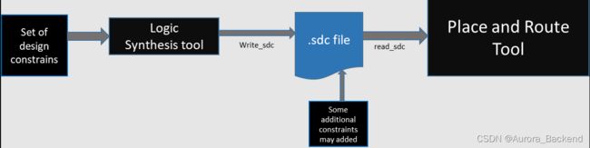
- Constraint file(Synopsys Design Constraints,SDC)
-
- 1. SDC Version
- 2. Units
- *System Interface
-
- 3. Set driving cells
- 4. Set load
- * Design Rule Constraints
-
- 5. Set maximum fanout
- 6. Set maximum transition:
- * Timing Constraints
-
- 7. Create clock
- 8. Create generated clock
- 9. Group path
- 10. Clock uncertainty
- 11. Clock latency
- 12. Input delay
- 13. Output delay
- * Timing Exceptions
-
- 14. Multicycle paths
- 15. False paths
- IO Interface Analysis: Constraints for IO pins on block level
- Input Interface
- Output Interface
design-related files
Remark: Team VLSI
Gate level netlist (design complier—synthesis)
综合后的门级网表:综合团队使用标准单元库和约束standard cell libraries and constraints对RTL 代码进行综合,并根据可用的标准单元将 RTL 代码转换为门级网表。此文件包含所有设计实例及其连接。
synthesis(综合和物理综合)
把(RTL)Register Transfer Level转换为Gate level netlist
综合的主流工具有两个,一个是Synopsys家的DC(Design Complier),另外一个是Cadence家的Genus。两个工具都可以使用物理综合的综合策略。综合后会生成gate level的netlist,然后就可以开始做设计导入工作了。
综合就是把Verilog、VHDL转换成网表的过程。综合按照是否考虑物理布局信息可分为逻辑综合和物理综合。逻辑综合通常用来做工艺较老的项目,或者较新工艺的面积和时序的评估。
综合需要设定约束条件,就是你希望综合出来的电路在面积,时序等目标参数上达到的标准。逻辑综合需要基于特定的综合库(工艺库),不同的库中,门电路基本标准单元(standard cell)的面积,时序参数是不一样的。所以,选用的综合库不一样,综合出来的电路在时序,面积上是有差异的。约束条件是人为加上去的,比如创建时钟,时钟频率等;工艺库是特定厂商提供。
物理综合需要读取floorplan的信息,综合工具通过这些floorplan信息就知道了设计大小、port和macro的摆放位置,基于此去做物理综合,其时序会更加贴近实际的情况,得到的网表质量也更高一点。物理综合得到的还是和前端RTL综合后的gate level netlist一样的.v文件,然后后续步骤就和按照正常flow从import design开始。

Synthesis flow

- Load library主要包括标准单元库以及IP核(SRAM等)文件
- Load design就是RTL代码,然后再加上时序约束
sdc,设计规则约束design rules constrains - 综合后分析是否达到性能指标,若满足,则写出database(可以放到Prime Time进行PR前的timing check,若可以则再进行PR)
Synthesis=Translation + Gate Mapping + Logic Optimization(转换+门级映射+逻辑优化)
Translation
Translates Verilog or VHDL descriptions into a generic technology (GTECH)netlist.which is an intermediate format中间格式 that can map to different manufactory’s library(TSMC,UMC…)
- 这一步与不同的foundary库无关,台积电(TSMC), 台湾,三星(Sansung), 韩国,格芯(Global Foundries), 美国,联电(UMC), 台湾,中芯国际(SMIC), 上海。
- Fabless 指的只从事芯片设计与销售,不从事生产的公司,这样的企业被成为“无厂化企业”,手机厂商中的华为、苹果和小米,还有高通和联发科,都属于 Fabless。
- IDM 就是指既能够自行设计、也能够自行生产的芯片厂商,世界上有这种能力的不多,我们熟知的只有三星和英特尔。
- Foundry 是能够自行完成芯片制造,但是没有设计能力的厂商,就是我们所熟知的代工厂。此时想到了农夫山泉的那句话:“我们不生产水,我们只是大自然的搬运工”。我们常说的台积电就是最为典型的 Foundry,
Gate Mapping
Mapping the GTECH netlist to the gate-level standard cells in target library( foundary library),like registers, AND,OR…
将工艺库中基本信息拿出来进行映射
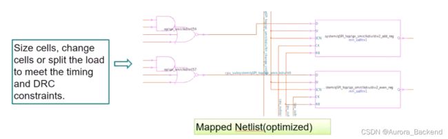
Logic Optimization
- Optimize the mapped gate-level standard cells to meet the timing,DRC constraints.(优化映射的门级标准单元,以满足时序要求)
- Timing constraints:Setup and hold,max/min delay.
- DRC constraints:max-transition,max-capacitance,max-fanout,max-leakage_power,
max-area.
调整单元大小、更改单元或拆分负载,以满足时序和DRC约束
Constraint file(Synopsys Design Constraints,SDC)
SDC is a short form of “Synopsys Design Constraint”. SDC is a common format for constraining the design which is supported by almost all Synthesis, PnR and other tools.Generally, timing, power and area constraints of design are provided through the SDC file and this file has extension .sdc.
SDC 文件的语法是基于 TCL 格式的,SDC 文件的所有命令都遵循 TCL 语法
In sdc file #is used to comment a line and ” is used to break the line. SDC file can be generated by the synthesis tool and the same can be used in for PnR.
在 sdc 文件中,一些重要的约束如下
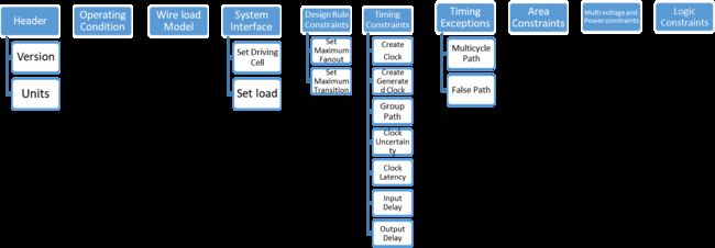
本文描述了SDC文件中的15个最重要的约束。对于复杂的设计,还有更多约束。
1. SDC Version
此语句指定 SDC 文件的版本。它可以是2.1、2.0、1.9或更老版本。
Version 2.1 has introduced in December 2017,Example:
set sdc_version 2.1
2. Units
- Units of various quantities(不同数量单位) like time, resistance, capacitance, voltage, current, and power can be specified using
set_unit command. - Multiples units can be set using a single set_unit command.Example:
set_units -time ns -resistance Kohm -capacitance pF -voltage V -current mA
m是10的负3次方量级,u是10的负6次方量级,n是10的负9次方量级,p是10的负12次方量级。kohm为千欧姆
SDC commands could be further categories as follow:
- Operating Conditions
- Wire Load Models
- System Interface
Let’s discuss some important System Interface constraints in this section.
*System Interface
3. Set driving cells
specifies the drive characteristics of input or inout ports that are driven by the cells in the technology library. These commands associate a library pin with input ports so that delay calculation can be accurately modelled.
指定由技术库中的单元驱动的输入或输出端口的驱动特性drive characteristics of input or inout ports that are driven by the cells。这些命令将库引脚与输入端口相关联associate a library pin with input ports,以便可以精确地计算延迟来建模These commands associate a library pin with input ports so that delay calculation can be accurately modelled.。
- Syntax:
set_driving_load [-lib_cell lib_cell_name] [-library lib_name] [-rise]
[-fall] [-min] [-max] [-pin pin_name] [-from_pin from_pin_name] [-dont_scale]
[-no_design_rule] [-input_transition_rise rtrans] [-input_transition_fall ftrans] [-multiply_by_facrtor] [-clock clock_name]
[-clock_fall] port_list
- Example:

set_driving_cell -lib_cell IV {I1}
set_driving_cell -lib_cell AND2 -pin Z -from_pin B {I2}
4. Set load
This command sets the load attributes(负载属性) on the specified ports and the nets in the current design.The unit of load value will be the unit of capacitance specified in the unit defined in this file.
- Syntax
set_load value objects [-subtract_pin_load] [-min] [-max] [[-pin_load] [-wire_load]]
- Example:
set_load -pin_load 0.001 [get_ports {port[10]}]
* Design Rule Constraints
In this part basically maximum fanout, maximum and minimum capacitance, and maximum transition time are set
5. Set maximum fanout
Maximum fanout load is set to a specific input port and/or design
- Syntax:
set_max_fanout fanout_value object_list
- Example:
set_max_fanout 5 [get_ports {port[10]}]
6. Set maximum transition:
Maximum transition time is set by this command which is a design rule and set to clock port or design is set to a specific input port and/or design.
- Syntax:
set_max_transition transition_value [-data_path] [-clock_path] object_list
- Example:
set_max_transition 2.5 [get_ports IN]
* Timing Constraints
In this part basically, we set clocks definition, clock group, clock latency, clock uncertainty, clock transition, input delay, output delay, timing derates etc.
7. Create clock
- Syntax:
create_clock [-name clock_name] [clock_sources] [-period value] [-waveform edge_list] [-add] [-comment]
The create_clock command creates a clock object in the current design. This command defines the specified source_objects as a clock source
- Example:

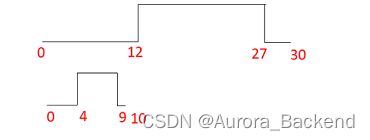
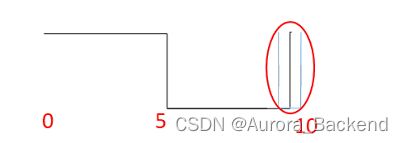
create_clock “u13/z” -name “CLK” -period 30 -waveform {12.0 27.0}

create_clock -name “PH12” -period 10 -waveform {0.0 5.0}
8. Create generated clock
- Syntax:
create_generated_clock [-name clock_name] [-add] source_objects -source master_pin
[-master_clock clock] [-divide_by divide_factor | -multiply_by multiply_factor ]
[-duty_cycle percent] [-invert] [-preinvert] [-edges edge_list] [-edge_shift edge_shift_list] [-combinational]
The create_generated_clock command creates a generated clock object. A pin or port could be specified for the generated clock object. Generated clock follows the master clock, so whenever the master clock changes generated clock will change automatically. A generated clock can be created as a frequency-divided clock, a frequency multiplied clock, an edge divided clock or an inverted clock.(分频时钟、倍频时钟、边沿分频时钟或反相时钟)
- Example:
create_generated_clock -multiplied_by 3 -source CLK [get_pins div3/Q]
The above example will generate a clock which is derived from the original clock named CLK. (原始时钟)
The generated clock will have a frequency 3 times of the original clock and time period will be one-third of the original (15ns –> 5ns).
9. Group path
 group_path [-weight weight_value] [-critical_range range_value] -default | -name group_name
 [-from from_list | -rise_from rise_from_list | -fall_from fall_from_list]
 [-through trough_list | -rise_through rise_through_list -fall_through fall_through_list]
 [-to to_list | -rise_to rise_to_list | -fall_to fall_to_list] [-comment comment_string] [-priority priority_level]
Groups are a set of paths or endpoints for the cost function calculations. The group enables us to specify a set of paths to optimize even though there may be a larger violation in other groups. When endpoints have been specified all paths leading to those end paths are grouped. (指定端点后,通向这些结束路径的所有路径都被分组。)
The create_clock command automatically creates a group for the new clock with a weight of 1.0 and named the same as the clock name.
自动为权重为1.0的新时钟创建一个组,并命名为与时钟名相同的名称。
- Example:
group_path -name “group1” -weight 2.0 -to {CLK1A CLK1B}group_path -name GROUP1 -from [get_ports ABC/in3] -to [get-ports FF1/D]
10. Clock uncertainty
- Syntax:
set_clock_uncertainity [object_list | -from from_clock | -rise_from rise_from_clock
| -fall_from fall_from_clock -to to_clock | -rise_to rise_to_clock | -fall_to fall_to_clock]
[rise] [-fall] [-setup] [-hold] uncertainty
After defining the clock, to take care of variance in the clock network clock uncertainty added. Clock uncertainty adds some margin of error into the system to account for variance in the clock network caused by non-ideality of clock network and clock source itself.Above specified command can specify either inter-clock uncertainty or simple uncertainty. It sets uncertainty to the worst skew expected to the endpoints or between the clock domains.
定义时钟后,要考虑到时钟的变化,在时钟网络中增加了时钟的不确定性。时钟不确定性给系统增加了一定的误差裕量,以弥补由于时钟网络和时钟源本身的不理想性而引起的时钟网络变化。以上指定的命令可以指定时钟间的不确定性或简单的不确定性。它将不确定性设置为预期到endpoint或时钟域之间的最坏偏差。
- Example:
关于clock_uncertainty的定义,一般由clock的jitter和slew来组成。对于-setup来说表示clock向前的偏移量,对于-hold来说表示clock向后的偏移量。
set_clock_uncertainty -setup 0.5 [get_clocks clk1]
set_clock_uncertainty -hold 0.2 [get_clocks clk1]
- 时钟的上升和下降时间
rise and fall time of the clock也可以添加不确定性Clock uncertainty,如下所示
set_clock_uncertainty -max_rise 0.12 [get_clocks clk1]
set_clock_uncertainty -max_fall 0.12 [get_clocks clk1]
set_clock_uncertainty -min_rise 0.12 [get_clocks clk1]
set_clock_uncertainty -min_fall 0.12 [get_clocks clk1]
在项目开始时,工艺厂会提供一个sign off guide,里面规定了setup、hold、transition的要求。在PR时的uncertainty、margin要比PT严格,如PT时的uncertainty为50ps,则PR的uncertainty为70ps。PT是Timing signoff工具,它必须严格按照foundary建议的signoff标准或者要求来做signoff,即setup 和hold的clock uncertainty都是定死的,这个是无法随意更改的。PT是验收工具,而PR是实现过程。所以只能通过调整PR阶段的clock uncertainty来让工具在PR阶段看到更大的timing violation,这样工具才会加大力度来优化这样的path。
PT和PR中的timing不一致,PR看到的结果过于乐观没有任何意义,因为验收工具是PT。只要PT中的timing不满足时序要求,就必须重新做或者做Timing ECO,所以尽量让PR比PT稍微严格个50ps左右是比较理想的。
11. Clock latency
- Syntax:
set_clock_latency [-rise] [-fall] [-min] [-max] [-source] [-early] [-late] [-dynamic jitter] [-clock clock_list] delay object_list
Clock latency specifies the amount of delay for a clock signal reaching to the clock pin of a sequential element from the clock source pin.
时钟延迟指定时钟信号从时钟源管脚到达时序元件的时钟管脚的延迟量。
There are two types of clock latency one is network latency (default) and the other is source latency (by using the -source option)
时序分析基本概念是Latency, 时钟传播延迟。主要指从Clock源到时序组件Clock输入端的延迟时间。它可以分为两个部分:时钟源插入延迟(source latency)和时钟网络延迟(network latency)。
关于clock_latency的定义,分为两部分:source latency和network latency。其中source latency 表示从clock source 到clock definition的path。network latency表示从clock definition到FF flip-flop的clock的clock pin的path。其中在CTS之后,network latency由set_propagated_clock来代替。
-
Timing path:
- valid start_point:input port和FF的clock input。
- valid end_point:output port和FF的data input。
-
一个valid的data_path是:
- 从input port到FF的data input。(in2reg)
- 从input port到output port。(feedthrough)
- 从FF的clock input到FF的data input。(reg2reg)
- 从FF的clock input到output port。(reg2out)
STA中所有的Timing path都由endpoint的clock来定义,如若没有,则为default path group。STA中的analysis和report都以clock为单位。
Clock network latency is the time taken by the clock signal to propagate(传播所花费时间) from the clock definition point to the clock pin of a register.
Whereas source latency is the time taken by a clock signal to propagate from actual-ideal waveform origin point(时钟源) to the clock definition point in the design. Source delay is also called an insertion delay.
- Example:
set_clock_latency 2.35 [get_pins ABC/XYZ/CP]
12. Input delay
set_input_delay delay_value [-reference_pin pin_port_name] [-clock clock_name] [-level_sensitive] [-network_latency_included] [-source-latency_included] [-rise] [-fall] [-min] [-max] [-add_delay] port_pin_list
Input delay defines the time requirements of an input port with respect to clock edge. Input ports are assumed to have zero input delay if it is not specified. The delay value to be specified is the delay between the start point and the object on which set_input_delay is being set relative to the clock edge.
输入延迟定义了输入端口相对于时钟沿的时间要求,如果未指定输入端口,则假定其输入延迟为零。
- Example:
set_input_delay -max 1.35 -clock clk1 {ain bin}
13. Output delay
- Syntax:
set_output_delay delay_value [-reference_pin pin_port_name] [-clock clock_name] [ -clock_fall] [-level_sensitive] [-network_latency_included] [-source-latency_included] [-rise] [-fall] [-min] [-max] [-add_delay] [-group_path group_name] port_pin_list
set_output_delay command sets output delay requirements on an output port with respect to the clock edge. Output ports are assumed to have zero output delay if it is not specified.
- Example:
set_output_delay 1.7 -clock [get_clocks CLK1] [all_outputs]
Above command will set output delay 1.7 unit to all output ports with respect to the positive edge (default edge) of the CLK1.
set_output_delay -max 1.4 -clock {CLK} [get_ports {Y}]

set_output_delay -min 1.0 -clock {CLK} [get_ports {Y}]
In above command -max value refers to the longest path and -min value refers to the shortest path. If no -max or -min value is specified, maximum and mimum output delays are assumed to be equal.
* Timing Exceptions
In this part, some of the important constraints like false paths, multicycle paths, maximum delay and minimum delay are defined.
虚假路径、多周期路径、最大延迟和最小延迟
14. Multicycle paths
- Syntax:
set_multicycle_path path_multiplier [-rise | -fall] [-setup | -hold] [-start | -end] [-from from_list | -rise_from rise_from_list | -fall_from fall_from_list] [-through through_list] [-rise_through rise_through_list] [-fall_through fall-through_list] [-to to_list | -rise_to rise_to_list | -fall_to fall_to_list] [-reset_path]
A multicycle path is an exception of the default single-cycle timing requirement path. In a multicycle path, signal requires more than one single clock cycle to propagate from the start point to the endpoint of the path.
在多周期路径中,信号需要一个以上的时钟周期才能从路径的起点传播到路径的终点
This command specifies the number of cycles the data path must have for setup or hold check. The following command will set a constraint of two cycles path from source point A to endpoint B.
- Example:
set_multicycle_path 2 -from A -to B
set_multicycle_path 3 -from C
We can add a -through point between source and endpoint and also we can set multicycle path to all paths my mentioning only source or only endpoint.
15. False paths
*Syntax:
set_false_path [-rise] [-fall] [-setup] [-hold] [-from from_list | -rise_from rise_from_list | -fall_from fall_from_list]
[-through through_list] [-rise_through rise_through_list] [-fall_through fall-through_list]
[-to to_list | -rise_to rise_to_list | -fall_to fall_to_list] [-reset_path]
A false path is a path that can not propagate a signal. For example, a path that is never activated by any combination of inputs is a false path. False paths should be disabled for timing analysis. The SDC command set_false_path is used to define the false paths. False paths will be excluded for timing analysis. (错误路径将被排除在时序分析之外。)
*Example:
set_false_path -from U1/G -to U1/D

set_false_path -from {ff12} -to {ff34}
IO Interface Analysis: Constraints for IO pins on block level
We all know that all the input and output pins of a block must be constrained in order to enable the PnR tool to optimize those interface paths. How to constrain an input or output pin will be discussed in this article. We will also discuss what are the actual meanings of these constraints and how these constraints affect the timing analysis.

在上图中,显示了两条时序路径timing paths,one is from CIN to FF1 and other is from FF2 to COUT. The path from CIN to FF1 is called input to register (In2Reg),whereas the path from FF2 to COUT is called register to output (Reg2Out) path. Any timing paths which are related to an input and output pins is called Interface timing path(时序接口路径).
Input Interface
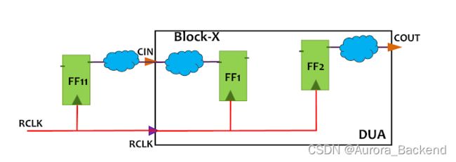
If we consider a block-level PnR implementation, the input to register path might be a part of the register to register path as shown in the above figure. Register FF11 is outside of the block but a part of the path from CIN to FF1 is inside the block. So in order to meet the timing of register to register path FF11 to FF1, we can divide this path into two parts.
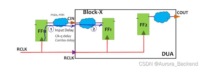
First part is the delay between the clock pin of FF11 to the input pin of block CIN, the second part is the delay from CIN pin to the D pin of FF1 as shown in the above figure. the first part is called input delay of the CIN pin. Since this path is out of the block so there is no timing information if this path can not be calculated by the tool. So we need to provide the delay of this part of the path as an input delay of pin CIN in SDC file.
Based on this input delay value PnR tool will estimate the timing margin from CIN to D pin of FF1 and optimize the path. On the block level, we need to close the timing from CIN to FF1 only that is Input to register path.
- Example:
- let’s say the clock period is 1ns.
- And for setup analysis, the data required time for
the path FF11 to FF1is 850ps. - Suppose the maximum delay of the path from
the clock pin of FF11 to CINis 550ps.(假设)
- Then on block-level, for setup analysis, we have to close the remaining path(剩余路径,即路径2) that is
from CIN to FF1at 850 – 550 = 300ps.
Input delay path has also two parts, one is clock to q dealy of FF11 and other is a combinational delay from q to CIN. This path will have max and min delay, which will be used separately in the setup and hold analysis. (最大和最小延迟分别用于setup和hold分析)。So when we apply input delay we apply two delays, max input delay and min input delay.
The command for applying this delayInput delay path in the SDC file is as follow.
- Setting Input Delay:
create_clock -name RLCK -period 1 [get_ports RCLK]

set_input_delay -max 0.55 -clock RCLK [get_ports CIN]

set_input_delay -min 0.45 -clock RCLK [get_ports CIN]
The above set of SDC commands will set the maximum input delay of 550 ps and minimum input delay 450 ps to CIN input pin. We can understand this in a more simple way that data will be launched from the CIN pin after the input delay. So more input delay means lesser time available to reach the data to capture flop FF1. A similar logic is applicable for hold analysis too.
Output Interface
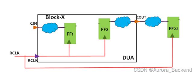
In block level, the register to output path from FF2 to COUT is a part of the complete path from FF2 to FF22 as shown in the above figure. Flip flop FF22 and the path from COUT to the FF22 is outside the block and this path can be supposed here a virtual path(虚拟路径).
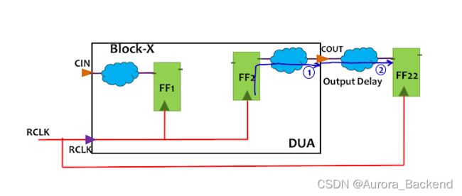
The path from FF2 to FF22 might be thought as two parts as shown in the above figure. part-1 is from FF2 to COUT which is inside the block and part-2 from COUT to FF22 which is outside the block and virtual here. Delay of part-2 path is called the output delay of the COUT pin. This delay is the combinational delay before the register FF22 and outside the block. This part will have a maximum and minimum delay which we need to specify while specifying the output delay for pin COUT.
- Example:
- let’s say the clock period is 1ns.
- And for setup analysis, the data required time for the path FF2 to FF22 is 800ps.
- Suppose the max delay of
the path-2 from COUT to FF22is 250ps.
- Then on block-level, for setup analysis, we have to close the remaining path from FF2 to COUT at 800 – 250 = 550ps.
In SDC file we specify maximum and minimum output delay, which is used separately for setup and hold analysis. The output delay is the delay from the output pin to the next register.
- Setting Output Delay:
create_clock -name RLCK -period 1 [get_ports RCLK]

set_output_delay -max 0.25 -clock RCLK [get_ports COUT]

set_output_delay -min 0.20 -clock RCLK [get_ports COUT]
The above set of SDC commands will set the maximum output delay of 250 ps and minimum input delay 200 ps to COUT output pin. We can imagine this like there is a virtual flop(虚拟的触发器) outside the block and the delay from COUT pin to that virtual flop is output delay of COUT pin. Here output delay has explained with reference to setup analysis but a similar concept is applicable for the hold analysis too.