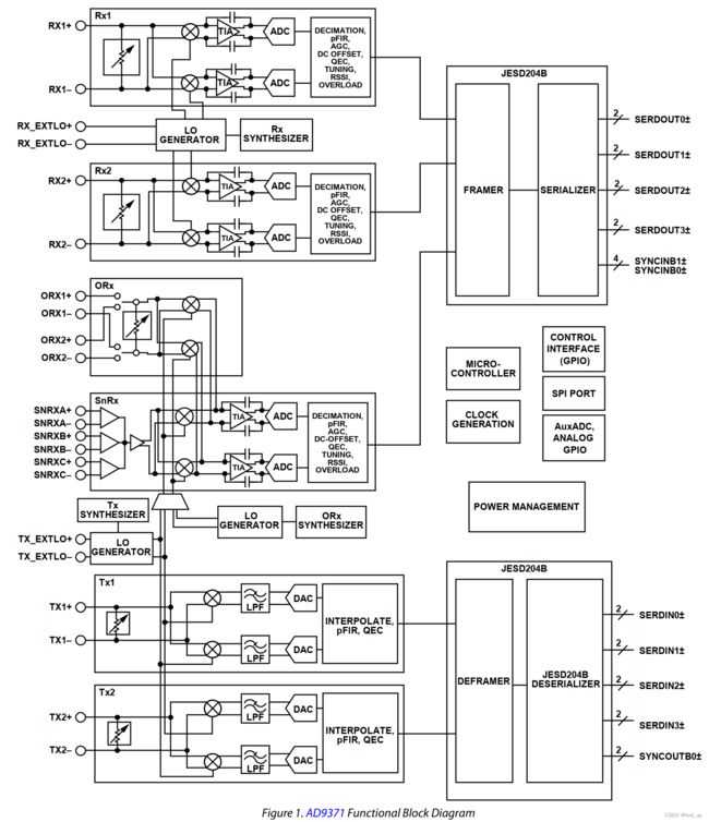
AD9371 官方例程裸机SW概述(一)
AD9371 系列快速入口
AD9371+ZCU102 移植到 ZCU106 : AD9371 官方例程构建及单音信号收发
ad9371_tx_jesd -->util_ad9371_xcvr接口映射: AD9371 官方例程之 tx_jesd 与 xcvr接口映射
AD9371 官方例程 时钟间的关系与生成 : AD9371 官方例程HDL详解之JESD204B TX侧时钟生成(一)
AD9371 官方例程 时钟间的关系与生成 : AD9371 官方例程HDL详解之JESD204B TX侧时钟生成 (二)
采样率和各个时钟之间的关系 : AD9371 官方例程HDL详解之JESD204B TX侧时钟生成 (三)
参考:
AD9371/AD9375 No-OS Setup
文章目录
- 前言
- 一、myk_ad9528init
- 二、myk.c
前言
SDK或者vitis 裸机程序需要配置 AD9528、AD9371、FPGA相关IP等,根据自己项目需求,可以通过 MATLAB Profile Generator 和 Transceiver Evaluation Software 生成所需的 myk.c, myk.h and myk_ad9528init.c 文件来替换
一、myk_ad9528init
AD9528 初始化文件

SPI 设置,通过SPI配置AD9528参数
1, //chip select Index ,AD9371 是 2,用于SPI 片选 spi_csn,ZYNQ只使用了 SPI0来配置9528和9371
static spiSettings_t clockSpiSettings = {
	1, //chip select Index
	0, //Write bit polarity
	1, //16bit instruction word
	1, //MSB first
	0, //Clock phase
	0, //Clock polarity
	0,//uint8_t enSpiStreaming;
	1,//uint8_t autoIncAddrUp;
	1 //uint8_t fourWireMode;
};
PLL1 相关配置
30720000,AD9258 PLL1 配置,refA 的频率
122880000,vcxo 频率,ADRV9371 板载的 122.88M
ad9528pll1Settings_t clockPll1Settings = {
	30720000,
	1,
	3,
	0,
	1,
	0,
	122880000,
	2,
	4
};
PLL2 相关配置
3,PLL2的M1,可选 3,4,5
PLL2的N2,应该为 10 ,这样 122.88M x 3 x 10 = 3.6864G ,满足PLL2的VCO工作频率 3.450 GHz 到 4.025 GHz
但没关系 ,主函数中的函数 AD9528_initDeviceDataStruct(clockAD9528_device,vcxo_Frequency,refA_Frequency,outFrequency[1])
会重新计算 PLL1 、 PLL2 和 SYSREF 的各个参数,得到 pll2Settings->n2Divider = 10
ad9528pll2Settings_t clockPll2Settings = {
	3,
	30
};
53237,00 1111 1111 0101,0 使能对应的OUT输出,53237 即 使能 OUT 1、3(SYSREF)、12(SYSREF)、13
{0,0,0,2,0,0,0,0,0,0,0,0,2,0}, 9528 OUT输出信号源 选择 outSource[3] = SYSREF;outSource[12] = SYSREF;
0,选择PLL2 经过 分频器 CHANNEL_DIV 产生信号
2,选择SYSREF generation 电路产生的 SYSREF 信号输出
最后一行是AD9528产生的 14路 输出信号频率,对于 ADRV9371 来说,使用了 OUT 1、3(SYSREF)、12(SYSREF)、13
outFrequency_Hz[1] 一定要设置成想得到的频率,以在 AD9528_initDeviceDataStruct 中使用,来计算各种参数
ad9528outputSettings_t clockOutputSettings = {
	53237,
	{0,0,0,2,0,0,0,0,0,0,0,0,2,0},
	{0,0,0,0,0,0,0,0,0,0,0,0,0,0},
	{0,0,0,0,0,0,0,0,0,0,0,0,0,0},
	{0,0,0,0,0,0,0,0,0,0,0,0,0,0},
	{10,10,10,10,10,10,10,10,10,10,10,10,10,10},
	{122880000, 122880000, 122880000, 122880000, 122880000, 122880000, 122880000, 122880000, 122880000, 122880000, 122880000, 122880000, 122880000, 122880000}
};
0,SPI,SYSREF requested 通过SPI请求 SYSREF , 1 通过 引脚
2,SYSREF 生成模式 ,2 内部产生,即 Mode 3 Internal
0,sysrefPatternMode_t,SYSREF 生成模式, N-shot = 0, CONTINUOUS = 1, PRBS = 2, STOP = 3
0,sysrefNshotMode_t ,SYSREF 输出脉冲数, ONE_PULSE = 0, TWO_PULSES = 2, FOUR_PULSES = 3
512, 16-bit K 分频 ,0 到 65535, 有一个固定 2分频,即最终分频 2 x k,如输入信号122.88M,SYSREF = 122.88M/(2 x 512)= 0.12 MHz ,得到SYSREF 频率为 120000, OUT 3 和 12 输出 0.12M 的 SYSREF 信号
ad9528sysrefSettings_t clockSysrefSettings = {
	0,
	2,
	0,
	0,
	0,
	0,
	512
};
myk_ad9528init文件 VCXO、REFA、outFrequency_Hz[1] 一定要设置对, PLL1、 PLL2、 SYSREF、Output 参数可以通过函数AD9528_initDeviceDataStruct 得到
二、myk.c
AD9371 初始化
AD9371内 TX 滤波器具体系数
static int16_t txFirCoefs[]
txFir 滤波器具体配置
6,滤波器增益
32, 使用多少抽头系数
static mykonosFir_t txFir = {
	6,              /* Filter gain in dB*/
	32,             /* Number of coefficients in the FIR filter*/
	&txFirCoefs[0]  /* A pointer to an array of filter coefficients*/
};
rx、obsrx、sniffer 同上

AD9371 RX 信号组帧配置,obsRxFramer 类似
2T2R,4个转换器,多帧有32个帧,解扰,使用外部 SYSREF 信号,0x03, 使用最低两个lane传输数据,
0 ,bitRepeat mode,RX 和 RX_OS(嗅探) 各自使用一个组帧器,采样率可以不一样,使用 Bit repeat 模式做到
0 ,/* Selects SYNCb input source,0 使用SYNCINB0(连到RX) , 1 使用SYNCINB1(连到OBSRX)
static mykonosJesd204bFramerConfig_t rxFramer = {
	0,              /* JESD204B Configuration Bank ID -extension to Device ID (Valid 0..15)*/
	0,              /* JESD204B Configuration Device ID - link identification number. (Valid 0..255)*/
	0,              /* JESD204B Configuration starting Lane ID.  If more than one lane used, each lane will increment from the Lane0 ID. (Valid 0..31)*/
	4,              /* number of ADCs (0, 2, or 4) - 2 ADCs per receive chain*/
	32,             /* number of frames in a multiframe (default=32), F*K must be a multiple of 4. (F=2*M/numberOfLanes)*/
	1,              /* scrambling off if framerScramble= 0, if framerScramble>0 scramble is enabled.*/
	1,              /* 0=use internal SYSREF, 1= use external SYSREF*/
	0x03,           /* serializerLanesEnabled - bit per lane, [0] = Lane0 enabled, [1] = Lane1 enabled*/
	0xE4,           /* serializerLaneCrossbar*/
	22,             /* serializerAmplitude - default 22 (valid (0-31)*/
	4,              /* preEmphasis - < default 4 (valid 0 - 7)*/
	0,              /* invertLanePolarity - default 0 ([0] will invert lane [0], bit1 will invert lane1)*/
	0,              /* lmfcOffset - LMFC_Offset offset value for deterministic latency setting*/
	0,              /* Flag for determining if SYSREF on relink should be set. Where, if > 0 = set, 0 = not set*/
	0,              /* Flag for determining if auto channel select for the xbar should be set. Where, if > 0 = set, '0' = not set*/
	0,              /* Selects SYNCb input source. Where, 0 = use RXSYNCB for this framer, 1 = use OBSRX_SYNCB for this framer*/
	0,              /* Flag for determining if CMOS mode for RX Sync signal is used. Where, if > 0 = CMOS, '0' = LVDS*/
	0,              /* Selects framer bit repeat or oversampling mode for lane rate matching. Where, 0 = bitRepeat mode (changes effective lanerate), 1 = overSample (maintains same lane rate between ObsRx framer and Rx framer and oversamples the ADC samples)*/
	0               /* Flag for determining if API will calculate the appropriate settings for framer lane outputs to physical lanes. Where, if '0' = API will set automatic lane crossbar, '1' = set to manual mode and the value in serializerLaneCrossbar will be used*/
};
AD9371 TX 信号解帧配置
2T2R,4个转换器,多帧有32个帧,加扰,使用外部 SYSREF 信号,0x0F, 使用全部 4 个lane传输数据,
0, /* LMFC_Offset offset,0…31,通过 LMFC 偏移调整确定性延迟
static mykonosJesd204bDeframerConfig_t deframer = {
	0,              /* bankId extension to Device ID (Valid 0..15)*/
	0,              /* deviceId  link identification number. (Valid 0..255)*/
	0,              /* lane0Id Lane0 ID. (Valid 0..31)*/
	4,              /* M  number of DACss (0, 2, or 4) - 2 DACs per transmit chain */
	32,             /* K  #frames in a multiframe (default=32), F*K=multiple of 4. (F=2*M/numberOfLanes)*/
	1,              /* scramble  scrambling off if scramble= 0.*/
	1,              /* External SYSREF select. 0 = use internal SYSREF, 1 = external SYSREF*/
	0x0F,           /* Deserializer lane select bit field. Where, [0] = Lane0 enabled, [1] = Lane1 enabled, etc */
	0xE4,           /* Lane crossbar to map physical lanes to deframer lane inputs [1:0] = Deframer Input 0 Lane section, [3:2] = Deframer Input 1 lane select, etc */
	1,              /* Equalizer setting. Applied to all deserializer lanes. Range is 0..4*/
	0,              /* PN inversion per each lane.  bit[0] = 1 Invert PN of Lane 0, bit[1] = Invert PN of Lane 1, etc).*/
	0,              /* LMFC_Offset offset value to adjust deterministic latency. Range is 0..31*/
	0,              /* Flag for determining if SYSREF on relink should be set. Where, if > 0 = set, '0' = not set*/
	0,              /* Flag for determining if auto channel select for the xbar should be set. Where, if > 0 = set, '0' = not set*/
	0,              /* Flag for determining if CMOS mode for TX Sync signal is used. Where, if > 0 = CMOS, '0' = LVDS*/
	0               /* Flag for determining if API will calculate the appropriate settings for deframer lane in to physical lanes. Where, if '0' = API will set automatic lane crossbar, '1' = set to manual mode and the value in deserializerLaneCrossbar will be used*/
};
RX 增益初始配置,orxGainControl 和 snifferGainControl 类似
MGC ,手动增益控制 ,AGC 自动增益控制
RSSI ,Rx1 RSSI 和 Rx2 RSSI
static mykonosRxGainControl_t rxGainControl = {
	MGC,            /* Current Rx gain control mode setting*/
	255,            /* Rx1 Gain Index, can be used in different ways for manual and AGC gain control*/
	255,            /* Rx2 Gain Index, can be used in different ways for manual and AGC gain control*/
	255,            /* Max gain index for the currently loaded Rx1 Gain table*/
	195,            /* Min gain index for the currently loaded Rx1 Gain table*/
	255,            /* Max gain index for the currently loaded Rx2 Gain table*/
	195,            /* Min gain index for the currently loaded Rx2 Gain table*/
	0,              /* Stores Rx1 RSSI value read back from the Mykonos*/
	0               /* Stores Rx2 RSSI value read back from the Mykonos*/
};
RX 自动增益 Peak threshold 模式参数配置 ,obsRxPeakAgc 类似
static mykonosPeakDetAgcCfg_t rxPeakAgc = {
	0x26,	/* apdHighThresh: */
	0x16,	/* apdLowThresh */
	0xB5,	/* hb2HighThresh */
	0x72,	/* hb2LowThresh */
	0x40,	/* hb2VeryLowThresh */
	0x06,	/* apdHighThreshExceededCnt */
	0x04,	/* apdLowThreshExceededCnt */
	0x06,	/* hb2HighThreshExceededCnt */
	0x04,	/* hb2LowThreshExceededCnt */
	0x04,	/* hb2VeryLowThreshExceededCnt */
	0x4,	/* apdHighGainStepAttack */
	0x2,	/* apdLowGainStepRecovery */
	0x4,	/* hb2HighGainStepAttack */
	0x2,	/* hb2LowGainStepRecovery */
	0x4,	/* hb2VeryLowGainStepRecovery */
	0x1,	/* apdFastAttack */
	0x1,	/* hb2FastAttack */
	0x1,	/* hb2OverloadDetectEnable */
	0x1,	/* hb2OverloadDurationCnt */
	0x1	/* hb2OverloadThreshCnt */
};
RX 自动增益 Power Measurement 模式参数 , obsRxPwrAgc 类似
static mykonosPowerMeasAgcCfg_t rxPwrAgc = {
	0x01,	/* pmdUpperHighThresh */
	0x03,	/* pmdUpperLowThresh */
	0x0C,	/* pmdLowerHighThresh */
	0x04,	/* pmdLowerLowThresh */
	0x4,	/* pmdUpperHighGainStepAttack */
	0x2,	/* pmdUpperLowGainStepAttack */
	0x2,	/* pmdLowerHighGainStepRecovery */
	0x4,	/* pmdLowerLowGainStepRecovery */
	0x08,	/* pmdMeasDuration */
	0x02	/* pmdMeasConfig */
};
RX AGC 配置 ,obsRxAgcConfig 类似
1, /* agcObsRxSelect , 1 选择 Sniffer
1, /* agcPeakThresholdMode ,1,Peak Threshold
static mykonosAgcCfg_t rxAgcConfig = {
	255,	/* agcRx1MaxGainIndex */
	195,	/* agcRx1MinGainIndex */
	255,	/* agcRx2MaxGainIndex */
	195,	/* agcRx2MinGainIndex: */
	255,	/* agcObsRxMaxGainIndex */
	203,	/* agcObsRxMinGainIndex */
	1,		/* agcObsRxSelect */
	1,		/* agcPeakThresholdMode */
	1,		/* agcLowThsPreventGainIncrease */
	30720,	/* agcGainUpdateCounter */
	3,	/* agcSlowLoopSettlingDelay */
	4,	/* agcPeakWaitTime */
	0,	/* agcResetOnRxEnable */
	0,	/* agcEnableSyncPulseForGainCounter */
	&rxPeakAgc,
	&rxPwrAgc
};

根据 Profile 文件 ,配置 rx、orx、sniffer、tx 的 IQ采样率 、信号带宽 、抽取或者内插系数、滤波器系数等
static mykonosTxProfile_t txProfile = {
	/* Tx 20/100MHz, IQrate 122.88MSPS, Dec5 */
	DACDIV_2p5,     /* The divider used to generate the DAC clock*/
	&txFir,         /* Pointer to Tx FIR filter structure*/
	2,              /* The Tx digital FIR filter interpolation (1,2,4)*/
	2,              /* Tx Halfband1 filter interpolation (1,2)*/
	1,              /* Tx Halfband2 filter interpolation (1,2)*/
	1,              /* TxInputHbInterpolation (1,2)*/
	122880,         /* Tx IQ data rate in kHz*/
	20000000,       /* Primary Signal BW*/
	100000000,      /* The Tx RF passband bandwidth for the profile*/
	710539,         /* The DAC filter 3dB corner in kHz*/
	50000,          /* Tx BBF 3dB corner in kHz*/
	0               /* Enable DPD, only valid for AD9373*/
};
9371 参考时钟

122.88M ,AD9525 OUT 13输出到9371的 DEV_CLK(E7 E8) , DEV_CLK参考时钟频率 10 MHz 到 320 MHz.
9830400 ,PLL VCO 工作频率,在 6 GHz 到 12 GHz
2,VCO divider,1,1.5,2,3, hsclkRate= clkPllVcoFrequency / VCO divider
4,HS Divider,4 或 5,hsDigClk = hsclkRate/ hsDiv
static mykonosDigClocks_t mykonosClocks = {
	122880,         /* CLKPLL and device reference clock frequency in kHz*/
	9830400,        /* CLKPLL VCO frequency in kHz*/
	VCODIV_2,       /* CLKPLL VCO divider*/
	4               /* CLKPLL high speed clock divider*/
};
RX 配置,txSettings 类似,Tx Attenuation ,衰减步长 和 衰减 mdB
RX1_RX2,初始化 RX 1 和 2
0, / Internal LO = 0, 本振使用内部产生的
2.5G,Rx PLL 本振频率 ,2.5GHz
0 , / 0,复数,1 实数
static mykonosRxSettings_t  rxSettings = {
	&rxProfile,     /* Rx datapath profile, 3dB corner frequencies, and digital filter enables*/
	&rxFramer,      /* Rx JESD204b framer configuration structure*/
	&rxGainControl, /* Rx Gain control settings structure*/
	&rxAgcConfig,   /* Rx AGC control settings structure*/
	RX1_RX2,        /* The desired Rx Channels to enable during initialization*/
	0,              /* Internal LO = 0, external LO*2 = 1*/
	2500000000U,    /* Rx PLL LO Frequency (internal or external LO)*/
	0               /* Flag to choose if complex baseband or real IF data are selected for Rx and ObsRx paths. Where, if > 0 = real IF data, '0' = zero IF (IQ) data*/
};
OBS_RX 配置,
MYK_ORX1_ORX2 | MYK_SNRXA_B_C,初始化 ORX1、ORX2、SNRXA、B、C
OBSLO_TX_PLL, Obs Rx 本振,0 本振由 Tx 产生, 1 本振由Sniffer 产生
2.6G,SnRx PLL 本振频率 ,2.6GHz
OBS_RXOFF , ObsRx 通道关闭,后续主函数中配置使用OBS_RX1_SNIFFERLO
MYKONOS_setObsRxPathSource(&mykDevice,OBS_RX1_SNIFFERLO)
typedef enum{
    OBS_RXOFF           = 0,
    OBS_RX1_TXLO        = 1,
    OBS_RX2_TXLO        = 2,
    OBS_INTERNALCALS    = 3,
    OBS_SNIFFER         = 4,
    OBS_RX1_SNIFFERLO   = 5,
    OBS_RX2_SNIFFERLO   = 6,
    OBS_SNIFFER_A       = 0x14,
    OBS_SNIFFER_B       = 0x24,
    OBS_SNIFFER_C       = 0x34
}

static mykonosObsRxSettings_t obsRxSettings = {
	&orxProfile,    /* ORx datapath profile, 3dB corner frequencies, and digital filter enables*/
	&orxGainControl,/* ObsRx gain control settings structure*/
	&obsRxAgcConfig,/* ORx AGC control settings structure*/
	&snifferProfile,/* Sniffer datapath profile, 3dB corner frequencies, and digital filter enables*/
	&snifferGainControl,/* SnRx gain control settings structure*/
	&obsRxFramer,   /* ObsRx JESD204b framer configuration structure */
	(MYK_ORX1_ORX2 | MYK_SNRXA_B_C),/* obsRxChannel */
	OBSLO_TX_PLL,   /* (obsRxLoSource) The Obs Rx mixer can use the Tx Synth(TX_PLL) or Sniffer Synth (SNIFFER_PLL) */
	2600000000U,    /* SnRx PLL LO frequency in Hz */
	0,              /* Flag to choose if complex baseband or real IF data are selected for Rx and ObsRx paths. Where if > 0 = real IF data, '0' = complex data*/
	NULL,           /* Custom Loopback ADC profile to set the bandwidth of the ADC response */
	OBS_RXOFF       /* Default ObsRx channel to enter when radioOn called */
};
SPI 参数配置
2, AD9371 是 2,9528 是1,用于SPI 片选 spi_csn,ZYNQ只使用了 SPI0来配置9528和9371
static spiSettings_t mykSpiSettings = {
	2, /* chip select index - valid 1~8 */
	0, /* the level of the write bit of a SPI write instruction word, value is inverted for SPI read operation */
	1, /* 1 = 16-bit instruction word, 0 = 8-bit instruction word */
	1, /* 1 = MSBFirst, 0 = LSBFirst */
	0, /* clock phase, sets which clock edge the data updates (valid 0 or 1) */
	0, /* clock polarity 0 = clock starts low, 1 = clock starts high */
	0, /* Not implemented in ADIs platform layer. SW feature to improve SPI throughput */
	1, /* Not implemented in ADIs platform layer. For SPI Streaming, set address increment direction. 1= next addr = addr+1, 0:addr=addr-1 */
	1  /* 1: Use 4-wire SPI, 0: 3-wire SPI (SDIO pin is bidirectional). NOTE: ADI's FPGA platform always uses 4-wire mode */
};
DPD, CLGC, 和 VSWR 功能只有AD9375有,dpdConfig,clgcConfig,vswrConfig 不用管
后续 和 AD9371 交互并未通过GPIO ,armGpio,gpio3v3,gpio,mykonosAuxIo 不用管
温度传感器见 tempSensor、tempStatus
主函数 和 FPGA 中的相关 IP配置见下一节