新一代硬件安全:第二章-静态伪装的可重配性
Chapter 2 Reconfigurability for Static Camouflaging
2.1 Chapter Introduction
Intellectual property (IP) piracy in the modern integrated circuit (IC) supply chain has necessitated countermeasures like layout camouflaging to safeguard proprietary design IP. Although effective initially, the conventional CMOS-centric layout camouflaging primitives hardly challenge attackers having access to advanced reverse engineering tools. Equipped with these state-of-the-art tools, which include de-layering and de-packaging equipment, scanning electron microscopy, and Boolean satisfiability (SAT)-based attacks, attackers can unmask the functionality of a camouflaged chip in minutes [EGT15]. The substantial overheads associated with CMOS-based camouflaging essentially limit its pervasive use across the chip [Raj+13b]. Emerging technologies could be a promising solution to this problem and enable the protection of a considerably larger portion of the design IP.
Static camouflaging, in particular, is achieved by reconfigurable emerging technologies that exhibit multiple device functionalities in the pre-fabrication stages. As the name implies, static camouflaging requires a device that can realize several Boolean functions but is programmed to implement only one of them at a time. Once set, the functionality remains static but unknown to the attacker since all the possible functions are accomplished with the same device layout. This contrasts with dynamic camouflaging, which requires a device capable of morphing its functionality multiple times on-the-fly. Static camouflaging is the preferred protection technique for high-performance deterministic processing systems, whereas dynamic camouflaging caters more to approximate computational circuits.
In this chapter, we present the fundamental concepts and considerations for constructing a static camouflaging primitive with emerging devices. We then examine three such devices and study how they were used to devise such a primitive.We also demonstrate a case study of an emerging device-based static camouflaging scheme, detailing the steps involved in the process, from conception to circuit implementation, and finally to security analysis.
2 静态伪装的可重配性
2.1 章节简介
在现代集成电路(IC)供应链中,针对知识产权(IP)盗版,需要采取诸如布局伪装等措施来保护专有设计知识产权。传统的以CMOS为中心的布局伪装基元在最初很有效,但随后很难抵挡攻击者使用高级逆向工程工具的攻击。配备这些最先进的工具,包括去分层和去封装设备、扫描电镜和基于布尔可满足性(SAT)攻击工具,攻击者可以在几分钟内撕开芯片的伪装[EGT15]。与基于CMOS的伪装相关的大量开销基本上限制了其在芯片中的广泛使用[Raj+13b]。新兴技术有望解决此类问题,并保护相当大一部分的设计知识产权。
静态伪装尤其是通过可重配新兴技术实现的伪装,在预制造阶段,使得元器件呈现多种功能性。顾名思义,静态伪装需要一个可实现多个布尔功能、但可编程为同一时间只能实现一个功能的元器件。一旦采用,其功能性仍然是静态的,但攻击者并不知情,因为所有可能的功能都是由同一元器件布局完成的。这与动态伪装形成鲜明对比,后者需要一种能够在运行中多次改变其功能的元器件。静态伪装是高性能确定性处理系统的首选保护技术,而动态伪装更适合近似计算电路。
本章首先介绍了使用新兴元器件构建静态伪装基元的基本概念和注意事项,随后调研了三个这样的新兴元器件,研究了它们是如何被用来设计这样的基元的,之后还演示分析了一个基于新兴元器件的静态伪装方案,详细说明了该过程中涉及到的步骤,从概念到电路实现,最后到安全分析。
2.2 Concepts for Static Camouflaging UsingReconfigurable Devices
Designing a secure and robust static camouflaging primitive hinges on selecting an emerging device, which can achieve reconfigurability. Reconfigurability, in this context, refers to the ability of a particular device to be configured as multiple logic functions without changing the underlying structure of the device. In the case of static camouflaging, this reconfigurability is only required in the pre-fabrication stages of the supply chain. We explore post-fabrication reconfigurability on-the-fly for dynamic camouflaging in the subsequent chapter. The important considerations for choosing a reconfigurable emerging device for static camouflaging are as follows:
- Multi-functional devices can realize several logic functions using one topology, wherein a control signal is typically used to program the functionality. Since the internal details of this control signal are unknown to the attacker, the functionality remains hidden. In the case of static camouflaging, the control signal is programmed once during the fabrication or testing phase and remains static throughout the lifetime of the circuit. However, the control signal could be programmed to one of the multiple possible states, resulting in different logic gates.
- For instance, several emerging logic technologies possess the capability to directly implement Majority (MAJ) logic in a single device, a feat that requires multiple gates in CMOS logic. By utilizing one of its inputs as a tie-breaking control input, an odd-input (emerging device-based) MAJ gate can be tuned to function as AND or OR. If the emerging device has intrinsic inversion, controllable via an external terminal, then NAND and NOR can be achieved as well.
- Some emerging device technologies enable the construction of optically indistinguishable circuit elements and gates, wherein an attacker cannot differentiate between the elements via optical imaging or inspection. Such devices generally produce identical layouts for the different gates implemented.
- Inserting dummy contacts is a secure design practice, which allows the designer to make multi-functional devices/gates optically indistinguishable at the layout level. The dummy contacts cover up any physical discrepancies in the wiring connections for the different versions of the multi-functional device, thus making them uniform. However, advanced imaging techniques that can detect the charge flow through contacts can decipher dummy contacts from real ones.
- Optically indistinguishable circuit elements are often forged from ambipolar emerging devices that can change their threshold voltage and majority carriers, by manipulating the channel doping. Since the doping level is not easily decoded by an attacker, the functionality remains hidden.
2.2 基于可重配元器件进行静态伪装的概念
设计一个安全可靠的静态伪装基元,取决于如何选择新兴元器件,以实现可重配性。在本文中,可重配性是指特定元器件可被配置为多个逻辑功能而不改变其底层结构的能力。在静态伪装的情况下,仅在供应链的预制阶段需要这种可重配性。下一章将探讨动态伪装在后制造阶段的运行时可重配性。如何选择用于静态伪装的可重配新兴元器件,重要的注意事项如下所述:
- 多功能性元器件可以使用一个拓扑实现多个逻辑功能,其中控制信号通常用于对功能进行编程。由于攻击者不知道该控制信号的内部细节,因此该功能仍处于隐藏状态。在静态伪装的情况下,控制信号在制造或测试阶段仅被编程一次,并且在电路的整个生命周期内保持静态。然而,控制信号可以被编程为多个可能状态之一,从而产生不同的逻辑门。
- 例如,一些新兴的逻辑技术具有在单个元器件中直接实现多数(MAJ)逻辑的能力,这需要CMOS逻辑中的多个门。通过将其一个输入用作仲裁的控制输入,奇数输入(基于新兴元器件)MAJ门可以被调谐为用作 AND 或 OR。如果新兴元器件具有可通过外部端子控制的本征反转,那么也可以实现 NAND 和 NOR。
- 一些新兴的元器件技术能够构建光学上不可区分(optically indistinguishable)的电路元件和门,攻击者无法通过光学成像或检测来区分这些元器件。这种元器件通常是采用相同的布局实现不同的门。
- 插入虚拟触点(dummy contact)是一种安全的设计实践,它允许设计者在布局层面上,使多功能性的元器件或门在光学上不可区分。虚拟触点屏蔽了多功能性元器件不同版本的接线连接中的任何物理差异,使之达到统一。然而,先进的可以检测流经触点的电荷流的成像技术,可以将虚拟触点与真实触点区分开来。
- 光学上不可区分的电路元件通常由双极性(ambipolar)新兴元器件制造而成,这些元器件可以通过操纵沟道掺杂来改变其阈值电压和多数载流子。由于掺杂程度不易被攻击者破译,因此其功能性仍能隐藏。
2.3 Review of Selected Emerging Technologies and Prior Art
In this section, we briefly review prior static camouflaging schemes, constructed with various classes of emerging devices and phenomena. This survey is intended to provide the reader with insights into how emerging multi-functional devices can be exploited to tackle IP piracy.
2.3 对所选新兴技术与现有技术的回顾
本节简要回顾了现有的静态伪装方案,这些方案由各种新兴元器件和现象构成。本调研旨在让读者深入了解如何利用新兴的多功能性元器件来解决IP盗版问题。
2.3.1 All-Spin Logic
The all-spin logic (ASL), introduced by Behtash et al. [Beh+10], was leveraged to build a static camouflaging primitive in [AYF17]. The ASL device utilizes non-local spin signals from nanomagnetic switching, to drive logic. The proposed camouflaging scheme can implement multi-functional ASL structures capable of realizing either NAND/NOR/AND/OR or XOR/XNOR or INV/BUF gates.
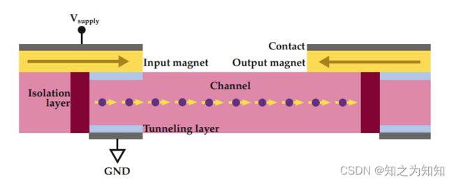
The basic ASL gate, shown in Fig. 2.1, consists of (1) two bistable magnetic free layers (input and output magnets), whose magnetization defines the binary state, (2) an isolation layer to separate different stages of the logic, (3) a non-magnetic channel to transport the spin signals from the input magnet to the output magnet, (4) a tunneling layer for the spins to tunnel from the input magnet into the channel, and (5) contacts to connect the supply and the ground. Here, the input and output ports of the magnets have low and high spin polarization factors, respectively. The channel is composed of a high spin-coherence length material like Cu.

The working of the basic ASL gate is as follows. A negative voltage on the input terminal will result in the injection of majority spins, parallel to the input magnet’s state, into the channel. This spin current switches the output magnet parallel to the input magnet, thus implementing the buffer (BUF) operation, whereas a positive voltage on the input terminal extracts majority spins from the channel, resulting in an opposite spin current that switches the output magnet anti-parallel with respect to the input magnet. This corresponds to the inversion (INV) operation. For further details on the construction and working of the ASL device, readers are referred to [Beh+10].
Majority logic is implemented in ASL by connecting several input terminals to one output terminal, wherein the output is dominated by the majority of the inputs. The authors in [AYF17] use a 3-input MAJ ASL structure with two primary inputs and one programmed tie-breaking key to realize complex Boolean gates. Here a key input of 0 implements the AND (positive supply voltage) and NAND (negative supply voltage) functions, whereas a key input of 1 results in OR (positive supply voltage) and NOR (negative supply voltage) gates. XOR and XNOR gates can be achieved in a 5-Terminal ASL structure through a sum of Full Adders operation, details of which can be found in [Aug+11].
Alasad et al. [AYF17] utilize this library of multi-functional ASL gates to demonstrate static camouflaging against brute force key search. However, their resilience against advanced SAT attacks is questionable, due to the small number of functions implemented with identical device layouts. Further, the relatively high energy overheads due to the ASL device impede the large-scale use of this scheme on real-world circuits.
2.3.1 全自旋逻辑
Behtash等人[Beh+10]引入的全自旋逻辑(ASL)被用于在[AYF17]中构建静态伪装基元。ASL器件利用来自纳磁体开关的非本地自旋信号来驱动逻辑,其所提出的伪装方案可以实现多功能ASL结构,该结构能实现 NAND / NOR / AND / OR 或 XOR / XNOR 或 INV / BUF门。
如图2.1所示,基本ASL门由(1)两个双稳态自由磁层(输入和输出磁体)组成,其磁化方向定义了二元状态;(2)隔离层,用于分离逻辑的不同阶段;(3)非磁性沟道,用于将自旋信号从输入磁体传输到输出磁体,(4)用于自旋从输入磁体隧穿到沟道中的隧穿层,以及(5)用于连接电源和地的触点。这里,磁体的输入和输出端口分别具有低和高自旋极化因子。该沟道由高自旋耦合长度材料如Cu组成。
基本ASL门的工作原理如下:输入端子上的负电压使得与输入磁体状态平行的大多数自旋注入沟道,该自旋电流使输出磁体平行于输入磁体,从而实现缓冲(BUF)操作,而输入端子上的正电压将从沟道中提取大部分自旋,从而产生相反的自旋电流,使得输出磁体反平行于输入磁体,这对应于反转(INV)操作。有关ASL器件的结构和工作原理的更多详细信息,请参阅[Beh+10]。
在ASL中,通过将多个输入端子连接到一个输出端子来实现多数逻辑,其中输出由多数输入控制。作者在[AYF17]中的使用了一个3-输入 MAJ ASL结构来实现复杂的布尔门,该结构具有两个主输入和一个可编程的仲裁信号,此处键入0将实现 AND(正电源电压)和 NAND(负电源电压)功能,而键入1则可得到 OR(正电源电压)和 NOR(负电源电压)门。XOR 和 XNOR 门可以在5-端ASL结构中通过全加法器运算实现,其详细信息可以在[88+11]中找到。
Alasad等人[AYF17]利用上述多功能ASL门的集合来演示针对暴力密钥搜索的静态伪装。然而,由于使用相同的器件布局实现的功能数量较少,其抵御高级SAT攻击的能力令人怀疑。此外,ASL器件造成的相对较高的能量开销,阻碍了该方案在实际电路中的大规模使用。
2.3.2 Silicon Nanowire Transistors
Silicon nanowire field effect transistors (SiNWFET) are viable devices for static camouflaging owing to their ambipolarity. As demonstrated by Bi et al. [Bi+14], the ability to switch the majority carrier type from n to p under normal bias conditions enables the reconfiguration of the device polarity to achieve multi-functionality. As illustrated in Fig. 2.2, they consider a vertically stacked SiNWFET structure with two gate-all around electrodes, the control gate and the polarity gate. The control gate is the conventional gate terminal, which switches the channel ON/OFF. The polarity gate, placed near the source/drain Schottky junctions, allows one to tune the device polarity.

Bi et al. propose a four SiNWFET layout for implementing NAND/NOR/XOR/XNOR functionalities, with different real and dummy contact configurations. This layout, detailed in [Bi+14], greatly reduces the area and power overheads as compared to similar camouflaging schemes in CMOS, which would require at least 12 transistors. However, the small number of functions implemented with the universal layout again hinders SAT resilience. This, in turn, would require a larger number of gates to be camouflaged, thus increasing overhead costs.
2.3.2 硅纳米线晶体管
硅纳米线场效应晶体管(SiNWFET)由于其双极性,是静态伪装的可行器件。如Bi等人在[Bi+14]中所示,在正常偏置条件下,将多数载流子类型从 n 切换到 p 的能力,可重新配置此器件的极性以实现多功能性。如图2.2所示,他们考虑了一种垂直堆叠的SiNWFET结构,该结构具有两个围绕电极的栅极,即控制栅极和极性栅极。控制栅极是常规的栅极端子,用于控制沟道的开/关。极性栅极放置在源极/汲极肖特基结附近,允许调谐器件极性。

Bi等人提出了一种四 SiNWFET 布局,用于实现 NAND / NOR / XOR / XNOR 功能,具有不同的实触点和虚触点配置。与CMOS中类似的需要至少12个晶体管的伪装方案相比,[Bi+14]中详述的这种布局极大减少了面积和功率开销。不过,因为通用布局中的功能实现较少,再次妨碍了其对SAT攻击的抗性,因此需要更多的门进行伪装,又因此增加了间接成本。
2.3.3 Two-Dimensional Devices
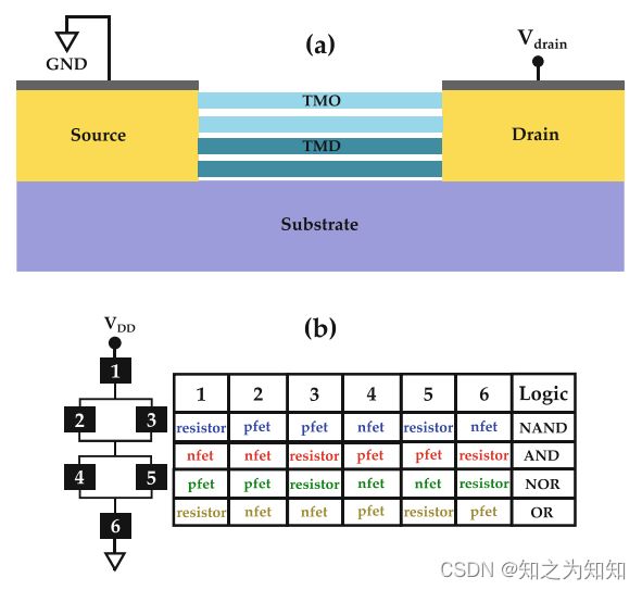
Wali et al. [Wal+21] proposed an advanced static camouflaging scheme by harnessing two-dimensional (2D) transition metal dichalcogenides (TMD) and transition metal oxides (TMO). The basic premise of their work hinges on the unique property of TMDs, wherein they can be molded into various circuit components, including nand p-type transistors, diodes, and resistors, using optically indistinguishable device structures. Plasma oxidation of the deposited TMD causes the oxidation of the top layers, resulting in substoichiometric TMOs that are optically transparent. This leaves behind a TMO/TMD heterostructure, which is partially transparent from the top, and resilient to optical inspection and analysis-based reverse engineering (RE). In fact, optical imaging-based techniques do not yield any information about the TMO thickness, plasma exposure time, or distinguishing color spectra in the TMO layers.
Their camouflaged resistor consists of a TMD/TMO heterostructure (Fig. 2.3a), which can implement various resistance values using the same device footprint and structure. The resistance can be adjusted by simply varying the plasma exposure time, which results in TMO layers of different thicknesses. However, the TMO being transparent is able to conceal this thickness and hence its resistance, from any attacker. The camouflaged diode is constructed by temporarily covering one side of the resistor heterostack by poly(methyl methacrylate), before introducing the oxygen plasma. This results in a diode junction, since the covered area remains intrinsic, while the exposed area is doped p-type owing to the substoichiometric TMO formation. Camouflaged transistors are achieved by leveraging the ambipolarity in the TMD/TMO heterostructure. As the plasma exposure time is increased, the heterostructure undergoes a change from n-type to p-type. This transformation does not leave any optical trace and both the n-type and p-type 2D-FETs are indistinguishable.

The camouflaged circuit elements are used in a black box configuration as shown in Fig. 2.3b, to realize various logic gates. Since the elements are identical, the gates constructed with them end up indistinguishable as well. The negligible overheads due to the intrinsic camouflaging property of these 2D heterostructures enable 100% camouflaging of all gates in the target circuit. This thwarts any brute force attack, and even advance SAT attacks are mitigated due to the increased attack time complexity. Further, automatic test pattern generation (ATPG) attacks, which rely on the targeted activation of specific gates and the subsequent propagation of their local outputs to the primary outputs, are rendered futile against this 2D devicebased camouflaging scheme. Note however that advanced RE setups employing a combination of Raman spectroscopy, atomic force microscopy, and scanning electron microscopy may be able to discern differences in the TMO layers, which could simplify the search space for RE.
2.3.3 二维器件
Wali等人在[Wal+21]中提出了一种先进的静态伪装方案,该方案用到二维(2D)过渡金属硫属化合物(TMD)和过渡金属氧化物(TMO),其工作的基本前提取决于TMD的独特性质,其中TMD可以模压制成各种电路组件,包括N和P型晶体管、二极管和电阻,均采用在光学上不可区分的器件结构。覆盖的TMD等离子体氧化使得顶层氧化,从而产生光学上透明的亚化学计量TMO,这将得到一个 TMO / TMD 异质结构,它的顶部部分透明,并且对基于光学探测和分析的逆向工程(RE)具有抗性。事实上,基于光学成像的技术不能获得诸如TMO厚度、等离子体曝光时间或TMO层中的区分色谱之类的信息。
伪装电阻由 TMD / TMO 异质结构组成(图2.3a),其器件占用空间和组成结构相同,但能实现不同的电阻值。电阻值的可调节是通过简单地改变等离子体暴露时间,生成不同厚度的TMO层来达到的。因为透明的TMO能够隐藏这种厚度,因此可以抵抗任何攻击。伪装二极管是通过在引入氧等离子体之前用聚甲基丙烯酸甲酯临时覆盖电阻异质结的一侧制成的。此种方式生成的二极管结,其覆盖区域保持原状,而暴露区域由于亚化学计量 TMO 的形成而掺杂p型。伪装晶体管是通过利用 TMD / TMO 异质结构中的双极性制成的。随着等离子体暴露时间的增加,异质结构经历从n型到p型的变化。这种变化不会留下任何光迹,并且n型和p型二维场效应晶体管都是不可区分的。
如图2.3b所示,伪装电路元件用于黑盒配置,以实现不同的逻辑门。由于元件是相同的,因此用它们构建的门最终也无法区分。由于这些2D异质结构固有的伪装特性,可以忽略不计的开销使得目标电路中的所有门都能够100%伪装。这可阻止任何暴力攻击,甚至由于攻击的时间复杂度的增加,高级SAT攻击情况也会得到缓解。此外,自动测试模式生成(ATPG)攻击依赖于特定门的目标激励以及从本地输出到原始输出的后续传播,对于这种基于二维器件的伪装方案来说,这种攻击没有效果。不过,请注意,配置了拉曼光谱、原子力显微镜和扫描电镜组合的高级逆向工程或许能够识别TMO层中的差异,简化其破解过程中的搜索空间。
2.4 Case Study: Static Camouflaging Using Giant Spin Hall Effect Devices
In [Pat+18b], Patnaik et al. proposed for the first time, a static camouflaging primitive that is capable of implementing all 16 possible Boolean functionalities 2.4 Case Study: Static Camouflaging Using Giant Spin Hall Effect Devices 41 for two inputs. With such a large solution space for the attacker to cover, even a modest 30–40% of circuit camouflaging renders SAT-based attacks computationally unfeasible. In this case study, we explore the different aspects and details of this primitive, to grasp the various steps involved in the design, implementation, and testing of a static camouflaging scheme.
The giant spin Hall effect (GSHE) switch, which is at the heart of the proposed primitive, is constructed by combining a heavy-metal spin Hall layer, such as tantalum, tungsten, platinum, or palladium, with a magnetic tunnel junction (MTJ) arrangement (Fig. 2.4). Above the heavy-metal layer are two nanomagnets for write and read modes (W-NM and R-NM, red). The W-NM is separated from the output terminal via an insulating oxide layer (green). On top of the R-NM sit two fixed ferromagnetic layers (dark green) with anti-parallel magnetization directions.

The switch relies on the spin Hall effect [Hir99] for generating and amplifying the spin current input, and the magnetic dipolar coupling phenomenon [Kan+15] to magnetically couple R-NM and W-NM, while keeping them electrically isolated. A charge current through the bottom heavy-metal layer (along xˆ) induces a spin current in the transverse direction (along yˆ), which is used to switch the magnetization state of the W-NM. The dipolar coupling field then causes the RNM to switch its orientation. That is because in the presence of magnetic dipolar coupling, the minimum energy state is the one in which the W-NM and the R-NM are anti-parallel to each other [DSB12]. The final magnetization state of the R-NM is read off using a differential MTJ setup. The logic (1 or 0) is encoded in the direction of the electrical output current (+I or −I). The current direction depends on the relative orientations of the fixed magnets in the MTJ stack with respect to the final magnetization of the R-NM. The parallel path offers a lower resistance for a charge current passing either from the MTJ contact to the output terminal or vice versa (i.e., from the output terminal to the MTJ contact). Hence, depending on the polarity of the read-out voltage applied to the low-resistance path (i.e., either V+ or V−), the output current either flows inward or outward, representing the logic encoding of the GSHE switch operation.
This basic GSHE device can readily implement a BUF or INV gate (buffer or inverter operations). To realize more complex multi-input logic gates, a tie-breaking control signal X with a fixed amplitude and polarity is applied in addition to the primary input signals at the input terminal. Note the input of the GSHE switch (or, more generally, any spin–orbit torque-driven magnetic switch) is additive in nature. The polarities of the control signal and the MTJ voltage polarities are used to permute between different Boolean operations (Fig. 2.5). See also Fig. 2.9 for all 16 possible Boolean gates.

The GSHE switch is a noisy polymorphic device, whose probability for output correctness depends on the input spin current’s amplitude and duration, i.e., the outputs generated by the previous logic stages. However, for static camouflaging the spin pulse amplitude and duration are set for deterministic switching.
2.4 案例研究: 使用巨型自旋霍尔效应器件进行静态伪装
在[Pat+18b]中,Patnaik等人首次提出了一种静态伪装基元,该基元能够实现2个输入的所有16种可能的布尔函数。由于攻击者需要遍历如此之大的解空间,即使是适度的30-40%的电路伪装也会使基于SAT的攻击在计算上变得不可行。本节探究了这个基元的各个方面和细节,以掌握静态伪装方案的设计、实现和测试所涉及的各个步骤。
巨型自旋霍尔效应(GSHE)开关是此基元的核心,它是通过将重金属自旋霍尔层(如钽、钨、铂或钯)与磁隧道结(MTJ)排列组合而成的,参见(图2.4)。重金属层上方是两个用于写入和读取模式的纳米磁体(W-NM 和 R-NM,红色)。W-NM通过绝缘氧化物层(绿色)与输出端子分离。在R-NM的顶部有两个固定的铁磁层(深绿色),磁化方向是反平行的。

此开关依赖于自旋霍尔效应[Hir99]来产生和放大自旋电流输入,并依赖磁偶极耦合现象[Kan+15]使 R-NM 和 W-NM 磁耦合,同时保持它们的电隔离。通过底部重金属层的电荷电流(沿 x ^ \hat{x} x^ 方向)在横向方向(沿 y ^ \hat{y} y^ 方向)感应出自旋电流,用于切换W-NM的磁化状态,然后偶极耦合场使 R-NM 改变其方向。这是因为在存在磁偶极耦合的情况下,最小能量状态是 W-NM 和 R-NM 彼此反平行的状态[DSB12]。R-NM 的最终磁化状态是用差分 MTJ 设置读取。逻辑(1 或 0)按照输出电流(+I 或 −I)的方向进行编码。电流方向取决于 MTJ 堆叠中固定磁体相对于 R-NM 的最终磁化的相对方向。并联通路为从 MTJ 触点传递到输出端子或相反(即,从输出端子传递到 MTJ 触点)的充电电流提供了较低的电阻。因此,根据施加到低电阻路径的读出电压的极性(即,V+ 或 V-),输出电流向内或向外的流动,表示 GSHE 开关操作的逻辑编码。
这种基本的 GSHE 器件可以很容易地实现 BUF 或 INV 门(缓冲器或反相器操作)。为了实现更复杂的多输入逻辑门,除了输入端子处的主输入信号之外,还施加具有固定幅度和极性的仲裁控制信号 X X X。注意,GSHE 开关(或更一般地,任何自旋轨道转矩驱动的磁性开关)的输入本质上是加性的。控制信号的极性和 MTJ 电压极性用于在不同布尔运算之间进行置换(图2.5)。所有16个可能的布尔门见图2.9。

GSHE 开关是一种有噪声的多态器件,其输出正确性的概率取决于输入自旋电流的幅值和持续时间,即前一逻辑级产生的输出。然而,对于静态伪装,自旋脉冲振幅和持续时间被设置为确定性变化。
2.4.1 Characterization and Comparison of the GSHE Switch
To quantify the overheads due to GSHE-based static camouflaging, it is important to evaluate the area, power, and delay metrics of a single device first. Patnaik et al. construct the layout of their GSHE switch (Fig. 2.6) based on the design rules for beyond-CMOS devices [NY13], in units of maximum misalignment length λ. The area of the GSHE switch is accordingly estimated to be 0.0016μm2.
The material parameters for the GSHE switch considered are given in Table 2.1. A spin current (IS) of at least 20μA is required for deterministic computing, whereas sub-critical currents are sufficient for probabilistic computing [Ran+17].
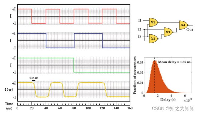
The performance of the switch is determined by nanomagnetic dynamics, simulated using the stochastic Landau–Lifshitz–Gilbert–Slonczewski equation [dAq+06]. Delay distributions for the nanomagnet considered are illustrated in Fig. 2.7. The mean propagation delay for deterministic computing is obtained as 1.55 ns, for IS = 20μA. This delay is then used to construct a behavioral Verilog model to obtain the transient responses shown in Fig. 2.8.


The power dissipation for the read-out phase is derived according to the equivalent circuit shown in Fig. 2.6 (inset). Using the following equations and the parameters listed in Table 2.1, the power dissipation of the GSHE switch for deterministic computing, including leakage, is derived as 0.2125μW.
Table 2.2 presents a comparison of GSHE switch against other emerging devicebased static camouflaging implementations. The higher delay of the GSHE switch is not prohibitive when used in conjunction with delay-aware logic synthesis and gate placement. As for security in terms of obfuscation, the number of possible functions is the relevant metric. Here, the GSHE switch significantly outperforms other devices.
The GSHE switch is leveraged for a versatile and effective security primitive— all 16 possible Boolean functions can be cloaked within a single device (Fig. 2.9). In other words, employing this primitive instead of regular gates can hinder RE attacks of the chip’s design IP, without the need for the designer to alter the underlying netlist. For example, to realize NAND/NOR using this primitive, three charge currents are fed into the bottom layer of the GSHE switch at once (Figs. 2.5 and 2.9): two currents represent the logic signals A and B, and the third current (X) acts as the “tie-breaking” control input. For some functions, the logic signals have to be provided as MTJ voltages, not as charge currents. To transduce voltage into charge currents (as well change their polarities), magnetoelectric (ME) transducers are used [Man+19, Ira+17]. These transducers, placed in the interconnects, are capable of charge current conversion (i.e., +I to −I) and voltage to charge current conversion (i.e., high/low voltages to ±I) and vice versa, with relatively low overheads.
Note that three wires must be used for the GSHE input terminals (Fig. 2.6). This is to render the primitive indistinguishable for imaging-based RE by malicious end-users, irrespective of the actual functionality. Several functionalities leave some of those wires unassigned (Fig. 2.9), which can be implemented as non-conductive dummy interconnects [Pat+17, CCW18], especially if only static camouflaging is considered.

To hinder fab-based adversaries, Patnaik et al. outline two promising options for secure implementation, either (1) leverage split manufacturing [McC11] or (2) provision for a tamper-proof memory. For option (1), the wires for the control inputs and the ferromagnet terminals are to remain protected from the untrusted FEOL fab. Hence, these wires have to be routed at least partially through the BEOL, which must be manufactured by a separate, trusted fab. For option (2), the tamper-proof memory holds a secret key that defines (using some additional circuitry) the correct assignment of control inputs and voltages for all devices. The key must be loaded (by the IP holder) into the memory only after fabrication.
For option (1), fab-based adversaries may employ proximity attacks to recover the withheld BEOL routing from various physical-design hints present in the FEOL [RSK13, Wan+16b]. However, the correct connection rate (which quantifies the BEOL recovery) tends to decrease for larger obfuscation scales. Further, for practically relevant camouflaging scales, the attack by Wang et al. [Wan+16b] incurs excessive runtime. For example, for 30% camouflaging of the benchmark b21, when split at M6, the attack cannot resolve within 48 h, resulting in a timeout. Overall, while some BEOL wires can be correctly inferred, proximity attacks are limited, especially when split at lower layers [Wan+16b, Pat+18f, MSD16, Sen+17, Pat+18e].
Both options (1) and (2) represent a notable advancement over prior work related to camouflaging, where the IP holder must trust the fab because of the circuit-level 2.4 Case Study: Static Camouflaging Using Giant Spin Hall Effect Devices 47 protection mechanism. In the remainder of this chapter, the focus will be on the threats imposed by malicious end-users.
2.4.1 GSHE 开关的表征与比较
为了量化基于 GSHE 的静态伪装造成的开销,首先评估单个器件的面积、功率和延迟指标是很重要的。Patnaik等人根据超 CMOS 器件的设计规则[NY13],以最大偏差长度 λ 为单位,绘制了他们的 GSHE 开关的布局(图2.6)。因此, GSHE 开关的面积估计为0.0016μm2。

表2.1给出了 GSHE 开关的材料参数考虑。确定性计算需要至少 20μA 的自旋电流(IS),而次临界电流足以进行概率计算[Ran+17]。

开关的性能由纳米磁动力学决定,并用随机 Landau–Lifshitz–Gilbert–Slonczewski 方程[dAq+06]进行模拟。纳米磁体的延迟分布的考虑如图2.7所示。当 I s = 20 μ A Is=20μA Is=20μA 时,确定性计算的平均传播延迟为1.55 ns。然后使用该延迟来构建行为 Verilog 模型,以获得图2.8所示的瞬态响应。

根据图2.6(插图)所示的等效电路,可推导出读出相位的功耗。使用以下方程和表2.1中列出的参数,可得出用于确定性计算(包括泄漏)的 GSHE 开关的功耗为0.2125μW。
表2.2 给出了 GSHE 开关与其他新兴的基于器件的静态伪装实现的比较。当与延迟感知逻辑合成和栅极放置结合使用时, GSHE 开关的较高延迟影响不大。至于混淆方面的安全性,可能混入的函数数量与相关的度量指标。在这里,GSHE 开关的性能明显优于其他器件。

GSHE 开关是一个通用且有效的安全基元——所有16个可能的布尔函数都可以隐藏在一个器件中(图2.9)。换句话说,使用该基元代替常规门,无需设计人员更改底层网表,即可以阻止芯片设计知识产权被逆向工程攻击。例如,为了使用该基元实现 NAND / NOR,三个电荷电流被同时馈送到 GSHE 开关的底层(图2.5和2.9):两个电流表示逻辑信号 A 和 B,第三个电流(X)充当仲裁控制输入。对于某些功能,逻辑信号必须作为 MTJ 电压而不是充电电流提供。为了将电压转换为充电电流(以及改变其极性),可使用磁电(ME)传感器[Man+19,Ira+17],放置在互连中的这些传感器能够进行充电电流转换(即,+I 到 -I)和电压到充电电流的转换(即高/低电压到±I),反之亦然,且开销相对较低。

请注意, GSHE 输入端子必须使用三根导线(图2.6),这是为了使来自恶意终端用户的、基于图像的逆向工程攻击无法区分此基元,不论其实际功能如何。一些功能保留了一些未分配的导线(图2.9),可实现为非导电虚拟互连[Pat+17,CCW18],特别是在仅考虑静态伪装的情况下。
为了阻止利用晶圆代工厂攻击的对手,Patnaik等人概述了安全实施的两个有前景的选项:(1)利用分割制造[Mc11]或(2)提供防篡改存储器。对于选项(1),控制输入和铁磁体端子的导线应由受信任的FEOL制造厂制造,必须至少部分通过BEOL布线,BEOL 也必须由一个独立的可信制造厂制造。对于选项(2),防篡改存储器内放置一个密钥,该密钥定义(有附加电路的)所有器件的控制输入和电压的正确赋值。密钥必须仅在这些器件制造后(由IP持有者)加载到存储器中。
对于选项(1),利用晶圆代工厂攻击的对手可以使用邻近攻击,从 FEOL 中存在的各种物理设计提示恢复被保留的 BEOL 路由[RSK13,Wan+16b]。不过,对于更大的混淆规模,正确的连接速率(可量化 BEOL 恢复速度)趋于下降。此外,对于实际相关的伪装尺度,Wang等人描述的攻击[Wan+16b]会导致过长的运行时间。例如,对于基准 b21 的 30% 伪装,当使用 M6 级分割时,攻击无法在 48 小时内解决,从而超时。总体而言,虽然可以正确推断出一些 BEOL 线,但接邻近攻击是有限的,尤其是在较低层分割时[Wan+16b,Pat+18f,MSD16,Sen+17,Pat+180e]。
选项(1)和(2)都代表了先前与伪装相关的工作的显著进步,先前IP持有者基于电路级别的保护机制都必须信任代工厂。本章接下来的部分,重点将放在恶意终端用户带来的威胁上。
2.4.2 Security Analysis
This section elaborates on the security of the GSHE static camouflaging primitive against various end-user attacks. Most notably, a comprehensive study for analytical SAT attacks is presented, which benchmarks the GSHE static camouflaging against prior art.
2.4.2 安全分析
本节详细介绍了 GSHE 静态伪装基元对各种终端用户攻击的安全性。特别是基于 GSHE 静态伪装与现有技术的对比,对可分析的 SAT 攻击进行了全面的研究。
2.4.2.1 Threat Model
The malicious end-user is interested in resolving the underlying IP implemented by the obfuscated chip. It is assumed that the attacker possesses the know-how and has access to equipment for imaging-based RE. However, the attacker does not have access to advanced capabilities for invasive read-out attacks, to resolve the voltage and current assignments for individual GSHE gates at runtime.
The attacker procures multiple copies of the chip from open market. They use one for RE, which includes de-packaging, de-layering, imaging of individual layers, stitching of these images, and final netlist extraction [Qua+16b]. The second one is employed as an oracle to obtain input–output (I/O) patterns. These patterns are then utilized for SAT-based attacks.
2.4.2.1 威胁模型
恶意终端用户想获得经过混淆的芯片的底层IP设计。假设攻击者拥有基于成像的逆向工程的专有技术和设备,但其仍无法在运行时获得单个 GSHE 门的电压和电流数据,因其不具备侵入式读取数据的高级攻击功能。
攻击者可从公开市场获取芯片的多个拷贝,其中一个用于逆向工程,包括去封装、去分层、单层成像、图像拼接和最终网表提取[Qua+16b],其余芯片可用来获得标准的输入输出(I/O)模式以用于基于 SAT 的攻击。
2.4.2.2 Reverse Engineering Attack Scenarios
Layout identification and read-out attacks: Since the physical layout of the GSHE static camouflaging primitive is uniform, it remains indistinguishable for optical imaging-based RE. It was also shown that dummy interconnects can become difficult to resolve during RE, as long as suitable materials such as Mg and MgO are used [Hwa+12, CCW18]. A more sophisticated attacker might, however, leverage electron microscopy for identification and read-out attacks. For example, Courbon et al. [CSW16] used scanning electron microscopy, in passive voltage contrast mode, to read out memories in secure chips. However, such attacks would prove significantly more difficult on the GSHE primitive owing to the minuscule dimensions of the GSHE switch, which diminishes spatial resolution for EM-based analysis [CSW16].
Magnetic- and Temperature-driven attacks: Ghosh et al. [Gho16] explore attacks on spintronic memory devices using external magnetic fields and malicious temperature curves. As for the GSHE switch, note that it is tailored for robust magnetic coupling (between the W and R nanomagnets) [Ran+17], and this coupling would naturally be disturbed by any external magnetic fields.Hence, an attacker leveraging a magnetic probe may induce stuck-at-faults. However, such malicious incursions are hardly controllable due to multiple factors. First, the extremely small size of the GSHE switch would require very large magnetic fields for the probe. Second, the attacker must know in advance the state of the nanomagnets, the orientation of the fixed magnets, and also the voltage polarities for the MTJ setup. Temperature-driven attacks will impact the retention time of the GSHE switch. The resulting disturbances, however, are stochastic due to the inherent thermal noise in the nanomagnets; fault attacks are accordingly challenging as well. As a result, subsequent sensitization attacks to resolve the obfuscated IP, as proposed in [Raj+13a], will be practically unfeasible.
2.4.2.2 逆向工程攻击场景
-
布局识别和读出攻击:由于 GSHE 静态伪装基元的物理布局是统一的,因此对于基于光学成像的逆向工程而言,它仍然无法区分。只要使用合适的材料(如Mg 和 MgO),逆向工程也无法解决虚拟互连的问题[Hwa+12,CCW18]。不过更老练的攻击者可能会利用电子显微镜进行识别和实施读出攻击,例如,Courbon等人在[CSW16]中提出,可在被动电压对比模式下,使用扫描电镜读取安全芯片中的存储器的内容。但因为 GSHE 开关的尺寸较小,会降低基于 EM 分析的空间分辨率,加大针对 GSHE 基元攻击的难度[CSW16]。
-
磁场和温度驱动的攻击:Ghosh等人在[Gho16]中探索了使用外部磁场和恶意温度曲线,对自旋电子存储器器件的攻击。至于 GSHE 开关,请注意它是为(W 和 R 纳米磁体之间的)鲁棒磁耦合[Ran+17]量身定制的,这种耦合天然会受到任何外部磁场的干扰,因此攻击者利用磁探针可能会出现卡顿故障。而且,由于多种因素,这种恶意入侵很难控制。首先, GSHE 开关的尺寸非常小,因此探头需要非常大的磁场。其次,攻击者必须事先知道纳米磁体的状态、固定磁体的方向以及 MTJ 设置的电压极性。温度驱动的攻击将影响 GSHE 开关的持续时间。然而,由于纳米磁体中固有的热噪声,产生的扰动是随机的,因此相应的故障攻击也具有挑战性。基于上述原因,后续[Raj+13a]中提出的解决混淆IP的敏化攻击实际上也是不可行的。
- Experimental setup: The GSHE static camouflaging primitive is modeled as outlined in [Yu+17]. More specifically, the logical inputs a and b are fed in parallel into all 16 possible Boolean gates, and the outputs of those gates are connected to a 16-to-1 MUX with four select/key bits. As for other prior art with less possible functionalities, a smaller MUX with less key bits may suffice. For a fair evaluation, the same set of gates are protected, i.e., gates are randomly selected once for each benchmark, memorized, and then the same selection is reapplied across all techniques. All the static camouflaging techniques are evaluated against powerful state-of-the-art SAT attacks [SRM15, Sub17], with time-out set to 48 h. The experiments are conducted on various benchmarks suites like ISCAS-85, MCNC, ITC-99, EPFL suite [Ama15], and the industrial IBM superblue suite [Vis+11].
- Insights on SAT-based attacks: Table 2.3 highlights the runtimes incurred by the seminal attack of Subramanyan et al. [SRM15, Sub17]. While there are further metrics such as the number of clauses, attack iterations, or number of remaining feasible assignments [Yu+17], runtime is a straightforward yet essential indicator—either an attack succeeds within the allocated time or not. It is observed that for the same number of gates protected, the more functions a primitive can cloak, the more resilient it becomes in practice. More importantly, the runtimes required for decamouflaging, if possible at all, tend to scale exponentially with the percentage of gates being camouflaged. The GSHE static camouflaging primitive induces by far the highest computational effort across all benchmarks. When over 30% of the circuit is camouflaged using the GSHE primitive, none of the benchmarks could be resolved within 48 h. Further analysis on full-chip protection using the GSHE primitive confirms this superior resilience.
- Delay optimization: Having investigated and benchmarked the SAT-resilience of GSHE-based static camouflaging, the final step in designing the primitive is to reconcile the considerable delay of the GSHE switch with the need to camouflage large parts of the target circuit. This can be done by implementing a delay-aware placement strategy, as outlined next. Large-scale circuits typically exhibit biased distributions of delay paths, with most paths having short delays but few paths having dominant critical delays (Fig. 2.10). If the CMOS gates in the non-critical paths are replaced with GSHE-based camouflaged gates, then the excessive delay overheads can be curtailed. On an average, 5–15% of all gates can be camouflaged this way. Conducting SAT attacks [SRM15, Sub17] on those protected designs yields no results within 240 h。

2.4.2.3 针对基于SAT的攻击的大尺度IP保护措施研究
-
实验设置: GSHE 静态伪装基元建模如[Yu+17]所述。更具体地说,逻辑输入 a 和 b 被并行馈送到一个有16种可能性的布尔门中,并且这些门的输出被连接到具有四个选择/键位的16-1 MUX上。对于现有的其他具有较少可能功能的技术,较少密钥位的较小MUX就足够了。为了评估的公平性,相同的一组门也受到保护,即每种技术基准随机选择一次门,记录,然后在所有技术中重新应用相同的选择。所有静态伪装技术都针对最先进的暴力SAT攻击[SRM15,Sub17]进行了评估,超时时间设置为48小时。实验在各种技术基准套件上进行,如ISCAS-85、MCNC、ITC-99、EPFL套件[Ama15]和工业级 IBM superblue套件[Vis+11]。
-
对基于SAT的攻击的认识:表2.3 着重指出了Subramanyan等人的开创性攻击触发的运行时间[SRM15,Sub17]变化。虽然还有更多的指标,如clause数量、攻击迭代次数或剩余可行取值数量[Yu+17],但运行时是一个简单但重要的指标,无论攻击是否在指定的时间内成功。据观察,对于相同数量的受保护的门,基元可以隐藏的功能越多,它在实践中就变得越有抗性。更重要的是,如果可行的话,解开伪装所需的运行时间往往会随着被伪装的门的百分比呈指数级增长。GSHE 静态伪装基元是迄今为止所有基准测试中计算量最高的。当超过30%的电路使用 GSHE 基元进行伪装时,48小时内无法完成任何基准测试。对使用 GSHE 基元进行全芯片保护的进一步分析证实了这种卓越的抗性。

-
延迟优化:在研究并测试了基于 GSHE 的静态伪装的SAT抗性之后,设计基元的最后一步是协调 由 GSHE 伪装的目标电路的规模所带来的延迟。这可以通过实施延迟感知放置策略来实现,如下所述。大规模电路通常呈现延迟路径的偏置分布,大多数路径具有短延迟,但很少有路径具有主要关键延迟(图2.10)。如果非关键路径中的 CMOS 门被基于 GSHE 伪装的门替换,则可以消减过多的延迟开销。平均而言,所有门中有5-15%可以通过这种方式进行伪装。在240小时内,对这些受保护的设计进行SAT攻击[SRM15,Sub17]不会产生任何结果。

2.5 Closing Remarks
In this chapter, we investigated how static camouflaging primitives are constructed with reconfigurable emerging devices. With advances in physics and materials engineering, new devices with even better camouflaging properties are expected in the near future. This chapter equips prospective security researchers with the necessary know-how to tap into the potential of these devices and formulate novel static camouflaging techniques. With the insights gained from this chapter, the readers can devise new primitives from scratch, from conception and selection of the appropriate emerging technology, to implementing the camouflaged cells and performing security analysis.
2.5 结束语
本章研究了如何使用可重配的新兴元器件构建静态伪装基元。随着物理学和材料工程的进步,预计在不久的将来会出现具有更好伪装特性的新器件。本章为未来的安全研究人员提供必要的知识储备,以挖掘这些器件的潜力,并形成新的静态伪装技术。通过本章获得的知识,读者可以从头开始设计新的基元,从构思和选择合适的新兴技术,到实现伪装单元及执行安全分析。
References
[Ama15] L. Amarù, Majority-Inverter Graph (MIG) Benchmark Suite (2015). http://lsi.epfl.ch/MIG
[Aug+11] C. Augustine et al., Low-power functionality enhanced computation architectureusing spin-based devices, in 2011 IEEE/ACM International Symposium on NanoscaleArchitectures (IEEE, Piscataway, 2011), pp. 129–136
[AYF17] Q. Alasad, J. Yuan, D. Fan, Leveraging all-spin logic to improve hardware security, inProceedings of the on Great Lakes Symposium on VLSI 2017 (2017), pp. 491–494
[Beh+10] B. Behin-Aein et al., Proposal for an all-spin logic device with built-in memory. Nat.Nanotechnol. 5(4), 266–270 (2010)
[Bi+14] Y. Bi et al., Leveraging emerging technology for hardware security-case study onSilicon Nanowire FETs and Graphene SymFETs, in 2014 IEEE 23rd Asian TestSymposium (IEEE, Piscataway, 2014), pp. 342–347 References 51
[Bi+16] Y. Bi et al., Emerging technology-based design of primitives for hardware security.J. Emerg. Tech. Comput. Syst. 13(1), 3:1–3:19 (2016). ISSN: 1550-4832. https://doi.org/10.1145/2816818
[CCW18] S. Chen, J. Chen, L. Wang, A chip-level anti-reverse engineering technique, in J.Emerg. Tech. Comput. Syst. 14(2), 29:1–29:20 (2018). ISSN: 1550-4832. https://doi.org/10.1145/3173462
[CSW16] F. Courbon, S. Skorobogatov, C. Woods, Direct charge measurement in floatinggate transistors of flash EEPROM using scanning electron microscopy, in Proc. Int.Symp. Test. Failure Analys. (2016), pp. 1–9. https://pdfs.semanticscholar.org/992a/20c0a8bb71642fc44fa65f053b3524113b99.pdf
[dAq+06] M. d’Aquino et al., Midpoint numerical technique for stochastic Landau-Lifshitz-Gilbert-dynamics. J. Appl. Phys. 99(8), 08B905 (2006)
[DSB12] S. Datta, S. Salahuddin, B. Behin-Aein, Non-volatile spin switch for Boolean andnon-Boolean logic. Appl. Phys. Lett. 101(25), 252411 (2012)
[EGT15] M. El Massad, S. Garg, M.V. Tripunitara, Integrated circuit (IC) decamouflaging:reverse engineering camouflaged ICs within minutes, in NDSS (2015), pp. 1–14
[Gho16] S. Ghosh, Spintronics and security: Prospects, vulnerabilities, attack models, andpreventions. Proceedings of the IEEE 104(10), 1864–1893 (2016)
[Hir99] J.E. Hirsch, Spin Hall effect. Phys. Rev. Lett. 83(9), 1834 (1999)
[Hwa+12] S.-W. Hwang et al., A physically transient form of silicon electronics. Science337(6102), 1640–1644 (2012). ISSN: 0036-8075. https://doi.org/10.1126/science.1226325. eprint: http://science.sciencemag.org/content/337/6102/1640.full.pdf
[HX15] Q. Hao, G. Xiao, Giant spin Hall effect and switching induced by spin-transfer torquein a W/Co40Fe40B20/MgO structure with perpendicular magnetic anisotropy. Phys.Rev. Appl. 3(3), 034009 (2015)
[HZ16] K. Huang, R. Zhao, Magnetic domain-wall racetrack memory-based nonvolatile logicfor low-power computing and fast run-time-reconfiguration. Trans. VLSI Syst. 24(9),2861–2872 (2016)
[Ira+17] R. Mousavi Iraei et al., Electrical-spin transduction for CMOS-spintronic interfaceand long-range interconnects. IEEE J. Explor. Solid-State Comput. Dev. Circ. 3, 47–55 (2017). ISSN: 2329-9231. https://doi.org/10.1109/JXCDC.2017.2706671
[Kan+15] N. Kani et al., A model study of an error-free magnetization reversal through dipolarcoupling in a two-magnet system. IEEE Trans. Magnet. 52(2), 1–12 (2015)
[Mae+11] H. Maehara et al., Tunnel magnetoresistance above 170% and resistance–area productof 1omga(μm)2 attained by in situ annealing of ultra-thin MgO tunnel barrier. Appl. Phys.Exp. 4(3), 033002 (2011)
[Man+19] S. Manipatruni et al., Scalable energy-efficient magnetoelectric spin–orbit logic.Nature 565(7737), 35–42 (2019)
[McC11] C. McCants, Trusted Integrated Chips (TIC). Tech. rep. Intelligence AdvancedResearch Projects Activity (IARPA), 2011
[MSD16] J. Magaña, D. Shi, A. Davoodi, Are proximity attacks a threat to the security ofsplit manufacturing of integrated circuits?, in Proc. Int. Conf. Comp.-Aided Des.Austin, Texas (2016), pp. 90:1–90:7. ISBN: 978-1-4503-4466-1. https://doi.org/10.1145/2966986.2967006
[Nir+16] I.R. Nirmala et al., A novel threshold voltage defined switch for circuit camouflaging,in Proc. Europe Test. Symp. (2016), pp. 1–2. https://doi.org/10.1109/ETS.2016.7519286
[NY13] D.E. Nikonov, I.A. Young, Overview of beyond-CMOS devices and a uniformmethodology for their benchmarking. Proc. IEEE 101(12), 2498–2533 (2013)
[Par+17] F. Parveen et al., Hybrid polymorphic logic gate with 5-terminal magnetic domainwall motion device, in Proc. Comp. Soc. Symp. VLSI (2017), pp. 152–157. https://doi.org/10.1109/ISVLSI.2017.3552 2 Reconfigurability for Static Camouflaging
[Pat+17] S. Patnaik et al., Obfuscating the Interconnects: Low-Cost and Resilient Full-ChipLayout Camouflaging, in Proc. Int. Conf. Comp.-Aided Des. (2017), pp. 41–48.https://doi.org/10.1109/ICCAD.2017.8203758
[Pat+18b] S. Patnaik et al., Advancing hardware security using polymorphic and stochastic spin-Hall effect devices, in 2018 Design, Automation & Test in Europe Conference &Exhibition (DATE) (IEEE, Piscataway, 2018), pp. 97–102
[Pat+18e] S. Patnaik et al., Concerted wire lifting: enabling secure and cost-effective splitmanufacturing, in Proc. Asia South Pac. Des. Autom. Conf. (2018), pp. 251–258.https://doi.org/10.1109/ASPDAC.2018.8297314
[Pat+18f] S. Patnaik et al., Raise your game for split manufacturing: restoring the truefunctionality through BEOL, in Proc. Des. Autom. Conf. (2018), pp. 140:1–140:6.https://doi.org/10.1145/3195970.3196100
[Qua+16b] S.E. Quadir et al., A survey on chip to system reverse engineering. J. Emerg. Tech.Comput. Syst. 13(1), 6:1–6:34 (2016). ISSN: 1550-4832. https://doi.org/10.1145/2755563
[Raj+13a] J. Rajendran et al., Security analysis of integrated circuit camouflaging, in Proc.Comp. Comm. Sec. Berlin, Germany (2013), pp. 709–720. ISBN: 978-1-4503-2477-9.https://doi.org/10.1145/2508859.2516656
[Raj+13b] J. Rajendran et al., Security analysis of integrated circuit camouflaging, in Proceed-ings of the 2013 ACM SIGSAC Conference on Computer & Communications Security(2013), pp. 709–720
[Ran+17] N. Rangarajan et al., Energy-efficient computing with probabilistic magnetic bits–performance modeling and comparison against probabilistic CMOS logic. IEEETrans. Magnetics 53(11), 1–10 (2017)
[RSK13] J. Rajendran, O. Sinanoglu, R. Karri, Is split manufacturing secure?, in Proc. Des.Autom. Test Europe (2013), pp. 1259–1264. https://doi.org/10.7873/DATE.2013.261
[Sen+17] A. Sengupta et al., Rethinking split manufacturing: an information-theoretic approachwith secure layout techniques, in Proc. Int. Conf. Comp.-Aided Des. (2017), pp.329–336. https://doi.org/10.1109/ICCAD.2017.8203796. Revised version available athttps://arxiv.org/abs/1710.02026
[SRM15] P. Subramanyan, S. Ray, S. Malik, Evaluating the security of logic encryptionalgorithms, in Proc. Int. Symp. Hardw.-Orient. Sec. Trust (2015), pp. 137–143. https://doi.org/10.1109/HST.2015.7140252
[Sub17] P. Subramanyan. Evaluating the Security of Logic Encryption Algorithms (2017).https://bitbucket.org/spramod/host15-logic-encryption
[Vis+11] N. Viswanathan et al., The ISPD-2011 routability-driven placement contest andbenchmark suite, in Proc. Int. Symp. Phys. Des. (2011), pp. 141–146
[Wal+21] A. Wali et al., Satisfiability attack-resistant camouflaged two-dimensional heterostruc-ture devices. ACS Nano 15(2), 3453–3467 (2021)
[Wan+16b] Y. Wang et al., The cat and mouse in split manufacturing, in Proc. Des. Autom. Conf.Austin, Texas (2016), pp. 165:1–165:6. ISBN: 978-1-4503-4236-0. https://doi.org/10.1145/2897937.2898104
[Win+16] T. Winograd et al., Hybrid STT-CMOS designs for reverse-engineering prevention, inProc. Des. Autom. Conf. (2016), pp. 88–93
[Yu+17] C. Yu et al., Incremental SAT-based reverse engineering of camouflaged logic circuits.Trans. Comput. Aided Des. Integr. Circ. Syst. 36(10), 1647–1659 (2017). ISSN: 0278-0070. https://doi.org/10.1109/TCAD.2017.2652220
[Zha+15] Y. Zhang et al., Giant spin Hall effect (GSHE) logic design for low power application,in Proc. Des. Autom. Test Europe (2015), pp. 1000–1005
[Zha16] J. Zhang, A practical logic obfuscation technique for hardware security. Trans. VLSISyst. 24(3), 1193–1197 (2016). ISSN: 1063-8210. https://doi.org/10.1109/TVLSI.2015.2437996