常见时钟约束(源同步)
数据路径:数据在整个传输起点和传输终点所经过的路径。
时钟路径:时钟从源端到达源端寄存器和目的寄存器的路径。通常由时钟源到源寄存器和时钟源到目的寄存器两条路径组成。
FPGA和外部芯片的同步通信接口,根据时钟来源可以分为系统同步接口和源同步接口。
FPGA与外部芯片之间的通信时钟都由外部同一时钟源(系统时钟)产生时,称为系统同步接口。(外部时钟分别给外部芯片和FPGA)
FPGA与外部芯片之间的通信时钟都是由源寄存器所在一侧(输出端产生),称为源同步接口。(从FPGA给到外部芯片、外部芯片给到FPGA)就是输入到FPGA的数据引脚,有对应的同步时钟信号也连接到FPGA引脚,并且在FPGA器件的内部也使用这个同步时钟信号去锁存该输入的数据信号。
时序分析的四种模型:
- reg——reg
- reg——pin
- pin——reg
- pin——pin
全局时钟网络是走的网 络节点,时钟到达每个寄存器的偏斜(skew)比较小,而自分频时钟走的是数据线,到达每个寄存器的延时不一样,跟布线就有关系。
Osc(振荡器)
Input_delay:发射延(lunch)到达数据开始的位置。
LrMax(lunch rise)越大,影响的是建立时间。
LrMin(lunch rise)越小,影响的是保持时间。
Output_delay:采样延(latch)到数据开始的位置。
约束顺序:
## Timing Assertions Section
# Primary clocks
# Virtual clocks
# Generated clocks
# Clock Groups
# Bus Skew constraints
# Input and output delay constraints
## Timing Exceptions Section
# False Paths
# Max Delay / Min Delay
# Multicycle Paths
# Case Analysis
# Disable Timing
## Physical Constraints Section
# located anywhere in the file, preferably before or after the timing constraints
# or stored in a separate constraint file
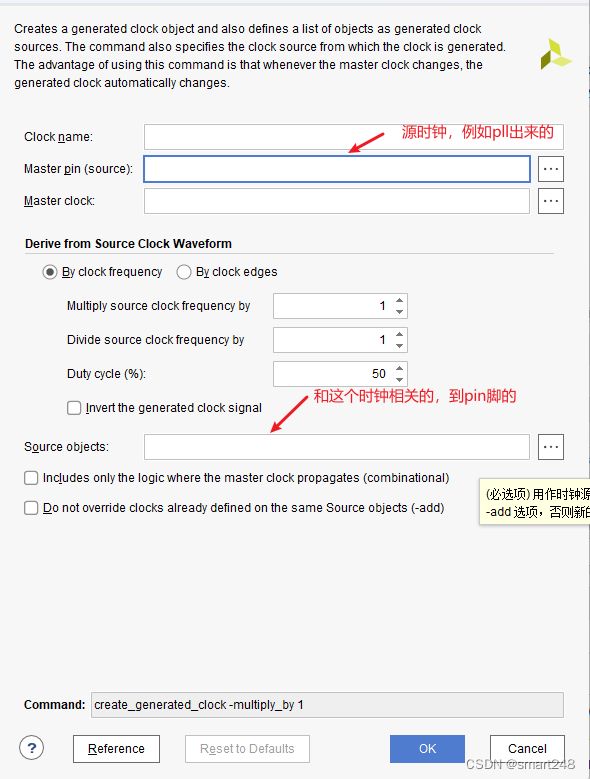
三类约束:
•Clocks
° Primary clocks
° Generated clocks
° Forwarded clocks
° External feedback delays
• Input and output ports
°
Input delays
° Output delays
° Combinatorial delays
• Clock domain crossings
° Physically exclusive clock groups
° Logically exclusive clock groups with no interaction
Logically exclusive clock groups with interaction
° Asynchronous clock domain crossings
• Constraints Summary
常见时序约束
- input_delay(以千兆网rx为例)
- 约束输入时钟,input_delay。

- 约束输入数据,通过indelay_control。

(* IODELAY_GROUP =
IDELAYCTRL IDELAYCTRL_inst (
.RDY(RDY), // 1-bit output: Ready output
.REFCLK(REFCLK), // 1-bit input: Reference clock input
.RST(RST) // 1-bit input: Active high reset input
);
IDELAYE2 #(
.CINVCTRL_SEL("FALSE"), // Enable dynamic clock inversion (FALSE, TRUE)
.DELAY_SRC("IDATAIN"), // Delay input (IDATAIN, DATAIN)
.HIGH_PERFORMANCE_MODE("FALSE"), // Reduced jitter ("TRUE"), Reduced power ("FALSE")
.IDELAY_TYPE("FIXED"), // FIXED, VARIABLE, VAR_LOAD, VAR_LOAD_PIPE
.IDELAY_VALUE(0), // Input delay tap setting (0-31)
.PIPE_SEL("FALSE"), // Select pipelined mode, FALSE, TRUE
.REFCLK_FREQUENCY(200.0), // IDELAYCTRL clock input frequency in MHz (190.0-210.0, 290.0-310.0).
.SIGNAL_PATTERN("DATA") // DATA, CLOCK input signal
)
IDELAYE2_inst (
.CNTVALUEOUT(CNTVALUEOUT), // 5-bit output: Counter value output
.DATAOUT(DATAOUT), // 1-bit output: Delayed data output
.C(C), // 1-bit input: Clock input
.CE(CE), // 1-bit input: Active high enable increment/decrement input
.CINVCTRL(CINVCTRL), // 1-bit input: Dynamic clock inversion input
.CNTVALUEIN(CNTVALUEIN), // 5-bit input: Counter value input
.DATAIN(DATAIN), // 1-bit input: Internal delay data input
.IDATAIN(IDATAIN), // 1-bit input: Data input from the I/O
.INC(INC), // 1-bit input: Increment / Decrement tap delay input
.LD(LD), // 1-bit input: Load IDELAY_VALUE input
.LDPIPEEN(LDPIPEEN), // 1-bit input: Enable PIPELINE register to load data input
.REGRST(REGRST) // 1-bit input: Active-high reset tap-delay input
);
如果refclk为200兆,那么每增加1,延迟为1/(32*2*200) us
注:一般专用芯片这个数据之间的skew很小,几乎是数据周期的 1/40 左右,比如 8ns 周期,data skew=8/40=0.2ns。
2.Output_delay

对于跨时钟域的信号一般不处理,因为我们已经使用了fifo去做跨时钟处理了,所以一般set false path。
Set multicycle path一些多周期的信号可以拉长它们的建立或者保持时间。

3.生成时钟