WinCE5.0 SMDK2410 BSP在GEC2410开发板上的移植(19)-Nand Flash驱动(FMD)及其简析(2)
接下来我们来看看对应的流接口驱动函数:
1.FMD_Init
FMD_Init进行了NAND控制器的初始化,复位Nand Flash(使用CMD_RESET命令),读FlashID看是否成功.具体参数命令见如下代码:
附上复位的时序图: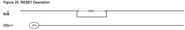
代码及注释如下:
PVOID FMD_Init(LPCTSTR lpActiveReg, PPCI_REG_INFO pRegIn, PPCI_REG_INFO pRegOut) { // Caller should have specified NAND controller address. // BOOL bLastMode = SetKMode(TRUE); if (pRegIn && pRegIn->MemBase.Num && pRegIn->MemBase.Reg[0]) s2410NAND = (S3C2410X_NAND_REG *)(pRegIn->MemBase.Reg[0]); else s2410NAND = (S3C2410X_NAND_REG *)NAND_BASE; // Set up initial flash controller configuration. // s2410NAND->NFCONF = (1 << 15) | /* Enable/Disable */ (1 << 14) | /* Page Size : 512Bytes */ (1 << 13) | /* 4 Step Address */ (1 << 12) | /* Initialize ECC */ (1 << 11) | /* nFCE control nFCE = HIGH */ (TACLS << 8) | /* CLE & ALE = HCLK * (TACLS + 1) */ (TWRPH0 << 4) | /* TWRPH0 = HCLK * (TWRPH0 + 1) */ (TWRPH1 << 0); /* TWRPH1 = HCLK * (TWRPH1 + 1) */ NF_nFCE_L(); // Select the flash chip. NF_CMD(CMD_RESET); // Send reset command. NF_WAITRB(); // Wait for flash to complete command. // Get manufacturer and device codes. if (ReadFlashID() != 0xEC76) { SetKMode (bLastMode); return(NULL); } NF_nFCE_H(); // Deselect the flash chip. SetKMode (bLastMode); return((PVOID)s2410NAND); }
2.FMD_EraseBlock
FMD_EraseBlock用来擦除单个Block块.使用CMD_ERASE,CMD_ERASE2命令,命令流程如下图:
时序图请参考datasheet.
代码及注释如下:
其中在原来SMDK2410BSP的fmd.cpp文件中,没有NF_CMD(CMD_STATUS);这句话,这将导致擦除操作无法成功.在CE6.0的DEVICEEMULATOR BSP中的fmd.cpp中已经有该命令,驱动可以直接使用.
BOOL FMD_EraseBlock(BLOCK_ID blockID) { BYTE Status; ULONG blockPage = (blockID * NAND_PAGE_CNT); // Convert block address to page address. BOOL bLastMode = SetKMode(TRUE); NF_nFCE_L(); // Select the flash chip. NF_CMD(CMD_ERASE); // Send block erase command. NF_ADDR(blockPage & 0xff); /* The mark of bad block is in 0 page */ NF_ADDR((blockPage >> 8) & 0xff); /* For block number A[24:17] */ NF_ADDR((blockPage >> 16) & 0xff); /* For block number A[25] */ NF_CMD(CMD_ERASE2); // Send block erase confirm command. NF_WAITRB(); // Wait for flash to complete command. NF_CMD(CMD_STATUS); //without this cmd, erase is not OK Status = NF_RDDATA(); // Read command status. //RETAILMSG(1,(TEXT("FMD: FMD_EraseBlock Status=0x%x/r/n"),Status)); NF_nFCE_H(); // Deselect the flash chip. SetKMode (bLastMode); return((Status & 1) ? FALSE : TRUE); }
3.FMD_ReadSector
FMD_ReadSector用来读取单个sector数据.CMD_READ命令用来读取sector512字节数据,CMD_READ2用来读取sector保留区数据(16字节)
READ流程图如下(READ2类型,Write 00h变为50h即可):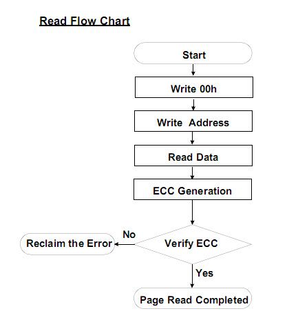
首先发送复位命令(CMD_RESET),然后根据pSectorBuff,pSectorInfoBuff是否有效来进行READ和READ2读取sector数据或sector保留区info数据.
如果读取sector数据,READ命令及sector地址发出后调用RdPage512Unalign或RdPage512(根据pSectorBuff是否字节对齐)来读调NAND数据.RdPage512Unalign和RdPage512用汇编来实现.
如果读取sector保留区数据,READ2命令及sector地址发出后,调用RdPageInfo来读保留区info数据,RdPageInfo同样由汇编来实现.
最后从NAND控制器读取相应的数据
整个读取过程在while循环下,根据要读取sector的个数dwNumSectors来读取指定数目sector的数据.
代码及注释如下:
BOOL FMD_ReadSector(SECTOR_ADDR startSectorAddr, LPBYTE pSectorBuff, PSectorInfo pSectorInfoBuff, DWORD dwNumSectors) { ULONG SectorAddr = (ULONG)startSectorAddr; BOOL bLastMode = SetKMode(TRUE); NF_RSTECC(); // Initialize ECC. NF_nFCE_L(); // Select the flash chip. NF_CMD(CMD_RESET); // Send reset command. while (dwNumSectors--) { ULONG blockPage = (((SectorAddr / NAND_PAGE_CNT) * NAND_PAGE_CNT) | (SectorAddr % NAND_PAGE_CNT)); NF_WAITRB(); // Wait for flash to complete command. if (pSectorBuff) { NF_CMD(CMD_READ); // Send read command. NF_ADDR(0); // Column = 0. NF_ADDR(blockPage & 0xff); // Page address. NF_ADDR((blockPage >> 8) & 0xff); NF_ADDR((blockPage >> 16) & 0xff); NF_WAITRB(); // Wait for command to complete. // Handle unaligned buffer pointer if( ((DWORD) pSectorBuff) & 0x3) { RdPage512Unalign (pSectorBuff); } else { RdPage512(pSectorBuff); // Read page/sector data. } NF_RDDATA(); // Read/clear status. NF_RDDATA(); // } if (pSectorInfoBuff) { NF_CMD(CMD_READ2); // Send read confirm command. NF_ADDR(0); // Column = 0. NF_ADDR(blockPage & 0xff); // Page address. NF_ADDR((blockPage >> 8) & 0xff); NF_ADDR((blockPage >> 16) & 0xff); NF_WAITRB(); // Wait for command to complete. RdPageInfo((PBYTE)pSectorInfoBuff); // Read page/sector information. NF_RDDATA(); // Read/clear status. NF_RDDATA(); // pSectorInfoBuff++; } ++SectorAddr; pSectorBuff += NAND_PAGE_SIZE; } NF_nFCE_H(); // Deselect the flash chip. SetKMode (bLastMode); return(TRUE); }
4.FMD_WriteSector
FMD_WriteSector用来写数据到指定sector.使用CMD_READ,CMD_WRITE或CMD_READ2,CMD_WRITE来写数据区(512字节)或info区(16字节保留区),Write流程图如下: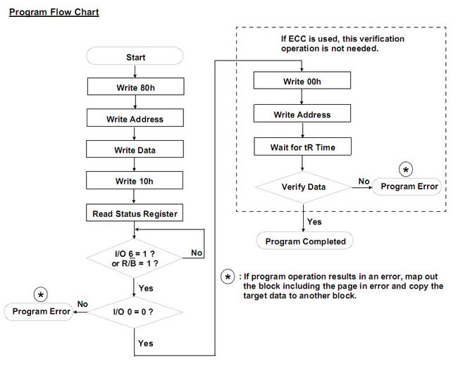
同Read操作一样,Write操作也区分是写sector数据还是sectorinfo数据.
写sectorinfo数据时,使用命令CMD_READ2,CMD_WRITE,然后调用WrPageInfo进行写sectorinfo数据.
写sector数据时,使用命令CMD_READ2,,CMD_WRITE,然后根据缓冲区是否对齐调用相应的WrPage512或WrPage512Unalign进行写sector数据,最后移动读数据指针(通过写FF给sectorinfo数据区),最后调用CMD_WRITE2和WrPageInfo完成写操作.同样进行while循环写指定sectors数目的数据.
WrPageInfo,WrPage512,WrPage512Unalign同样是用汇编实现的.
代码及注释如下:
BOOL FMD_WriteSector(SECTOR_ADDR startSectorAddr, LPBYTE pSectorBuff, PSectorInfo pSectorInfoBuff, DWORD dwNumSectors) { BYTE Status; ULONG SectorAddr = (ULONG)startSectorAddr; BOOL bLastMode = SetKMode(TRUE); if (!pSectorBuff && !pSectorInfoBuff) return(FALSE); NF_RSTECC(); // Initialize ECC. NF_nFCE_L(); // Select the flash chip. while (dwNumSectors--) { ULONG blockPage = (((SectorAddr / NAND_PAGE_CNT) * NAND_PAGE_CNT) | (SectorAddr % NAND_PAGE_CNT)); if (!pSectorBuff) { // If we are asked just to write the SectorInfo, we will do that separately NF_CMD(CMD_READ2); // Send read command. NF_CMD(CMD_WRITE); // Send write command. NF_ADDR(0); // Column = 0. NF_ADDR(blockPage & 0xff); // Page address. NF_ADDR((blockPage >> 8) & 0xff); NF_ADDR((blockPage >> 16) & 0xff); WrPageInfo((PBYTE)pSectorInfoBuff); pSectorInfoBuff++; } else { NF_CMD(CMD_READ); // Send read command. NF_CMD(CMD_WRITE); // Send write command. NF_ADDR(0); // Column = 0. NF_ADDR(blockPage & 0xff); // Page address. NF_ADDR((blockPage >> 8) & 0xff); NF_ADDR((blockPage >> 16) & 0xff); // Special case to handle un-aligned buffer pointer. if( ((DWORD) pSectorBuff) & 0x3) { WrPage512Unalign (pSectorBuff); } else { WrPage512(pSectorBuff); // Write page/sector data. } // Write the SectorInfo data to the media. // if(pSectorInfoBuff) { WrPageInfo((PBYTE)pSectorInfoBuff); pSectorInfoBuff++; } else // Make sure we advance the Flash's write pointer (even though we aren't writing the SectorInfo data) { BYTE TempInfo[] = {0xFF, 0xFF, 0xFF, 0xFF, 0xFF, 0xFF, 0xFF, 0xFF}; WrPageInfo(TempInfo); } pSectorBuff += NAND_PAGE_SIZE; } NF_CMD(CMD_WRITE2); // Send write confirm command. NF_WAITRB(); // Wait for command to complete. NF_CMD(CMD_STATUS); Status = NF_RDDATA(); if (Status & 1) { SetKMode (bLastMode); return(FALSE); } ++SectorAddr; } NF_nFCE_H(); // Deselect the flash chip. SetKMode (bLastMode); return(TRUE); }
5.其他流接口函数
对应于流接口驱动的其他几个函数,如FMD_PowerUp,FMD_PowerDown,FMD_OEMIoControl,FMD_Deinit均未实现.
6.最后来看看汇编实现的几个函数
RdPage512,RdPage512Unalign,WrPage512,WrPage512Unalign,WrPageInfo
这里就不多介绍了,主要的还是load,set的操作,可以参考ARM指令集
汇编代码如下:
; ; Copyright (c) Microsoft Corporation. All rights reserved. ; ; ; Use of this source code is subject to the terms of the Microsoft end-user ; license agreement (EULA) under which you licensed this SOFTWARE PRODUCT. ; If you did not accept the terms of the EULA, you are not authorized to use ; this source code. For a copy of the EULA, please see the LICENSE.RTF on your ; install media. ; ; ; NAND(SmartCard) Related Routines ; INCLUDE kxarm.h TEXTAREA MACRO LDR4STR1 $src, $tmp1, $tmp2 ldrb $tmp1, [$src] ldrb $tmp2, [$src] orr $tmp1, $tmp1, $tmp2, lsl #8 ldrb $tmp2, [$src] orr $tmp1, $tmp1, $tmp2, lsl #16 ldrb $tmp2, [$src] orr $tmp1, $tmp1, $tmp2, lsl #24 MEND MACRO STR4LDR1 $tgt, $src strb $src, [$tgt] mov $src, $src, lsr #8 strb $src, [$tgt] mov $src, $src, lsr #8 strb $src, [$tgt] mov $src, $src, lsr #8 strb $src, [$tgt] MEND ; Read one sector. Buffer (r0) must be aligned. ; LEAF_ENTRY RdPage512 stmfd sp!,{r1 - r11} ldr r1, =0xb0e0000c ;NFDATA mov r2, #0x200 1 LDR4STR1 r1, r4, r3 LDR4STR1 r1, r5, r3 LDR4STR1 r1, r6, r3 LDR4STR1 r1, r7, r3 LDR4STR1 r1, r8, r3 LDR4STR1 r1, r9, r3 LDR4STR1 r1, r10, r3 LDR4STR1 r1, r11, r3 stmia r0!, {r4 - r11} subs r2, r2, #32 bne %B1 ldmfd sp!, {r1 - r11} IF Interworking :LOR: Thumbing bx lr ELSE mov pc, lr ; return ENDIF ; Read one sector. Handles case where buffer (r0) is unaligned. ; LEAF_ENTRY RdPage512Unalign stmfd sp!,{r1 - r12} ldr r1, =0xb0e0000c ;NFDATA mov r2, #480 ; Calculate number of unaligned bytes to read (r12 = 4 - (r0 & 3)) and r12, r0, #3 rsb r12, r12, #4 mov r3, r12 rd_unalign1 ; Read unaligned bytes ldrb r4, [r1] strb r4, [r0] add r0, r0, #1 subs r3, r3, #1 bne rd_unalign1 rd_main ; Read 480 bytes (32 x 15) LDR4STR1 r1, r4, r3 LDR4STR1 r1, r5, r3 LDR4STR1 r1, r6, r3 LDR4STR1 r1, r7, r3 LDR4STR1 r1, r8, r3 LDR4STR1 r1, r9, r3 LDR4STR1 r1, r10, r3 LDR4STR1 r1, r11, r3 stmia r0!, {r4 - r11} subs r2, r2, #32 bne rd_main ; Read 28 bytes LDR4STR1 r1, r4, r3 LDR4STR1 r1, r5, r3 LDR4STR1 r1, r6, r3 LDR4STR1 r1, r7, r3 LDR4STR1 r1, r8, r3 LDR4STR1 r1, r9, r3 LDR4STR1 r1, r10, r3 stmia r0!, {r4 - r10} ; Read trailing unaligned bytes rsbs r12, r12, #4 beq rd_exit rd_unalign2 ldrb r4, [r1] strb r4, [r0] add r0, r0, #1 subs r12, r12, #1 bne rd_unalign2 rd_exit ldmfd sp!, {r1 - r12} IF Interworking :LOR: Thumbing bx lr ELSE mov pc, lr ; return ENDIF ; Write one sector. Buffer (r0) must be aligned. ; LEAF_ENTRY WrPage512 stmfd sp!,{r1 - r11} ldr r1, =0xb0e0000c ;NFDATA mov r2, #0x200 1 ldmia r0!, {r4 - r11} STR4LDR1 r1, r4 STR4LDR1 r1, r5 STR4LDR1 r1, r6 STR4LDR1 r1, r7 STR4LDR1 r1, r8 STR4LDR1 r1, r9 STR4LDR1 r1, r10 STR4LDR1 r1, r11 subs r2, r2, #32 bne %B1 ldmfd sp!, {r1 - r11} IF Interworking :LOR: Thumbing bx lr ELSE mov pc, lr ; return ENDIF ; Writes one sector. Handles case where buffer (r0) is unaligned. ; LEAF_ENTRY WrPage512Unalign stmfd sp!,{r1 - r11} ldr r1, =0xb0e0000c ;NFDATA mov r2, #480 ; Calculate number of unaligned bytes to read (r12 = 4 - (r0 & 3)) and r12, r0, #3 rsb r12, r12, #4 mov r3, r12 wr_unalign1 ; Write unaligned bytes ldrb r4, [r0] strb r4, [r1] add r0, r0, #1 subs r3, r3, #1 bne wr_unalign1 wr_main ; Write 480 bytes (32 x 15) ldmia r0!, {r4 - r11} STR4LDR1 r1, r4 STR4LDR1 r1, r5 STR4LDR1 r1, r6 STR4LDR1 r1, r7 STR4LDR1 r1, r8 STR4LDR1 r1, r9 STR4LDR1 r1, r10 STR4LDR1 r1, r11 subs r2, r2, #32 bne wr_main ; Write 28 bytes ldmia r0!, {r4 - r10} STR4LDR1 r1, r4 STR4LDR1 r1, r5 STR4LDR1 r1, r6 STR4LDR1 r1, r7 STR4LDR1 r1, r8 STR4LDR1 r1, r9 STR4LDR1 r1, r10 ; Write trailing unaligned bytes rsbs r12, r12, #4 beq wr_exit wr_unalign2 ldrb r4, [r0] strb r4, [r1] add r0, r0, #1 subs r12, r12, #1 bne wr_unalign2 wr_exit ldmfd sp!, {r1 - r11} IF Interworking :LOR: Thumbing bx lr ELSE mov pc, lr ; return ENDIF ; Read page/sector information. This includes logical sector number ; and block status flags (RO, OEM-defined, etc.). ; LEAF_ENTRY RdPageInfo stmfd sp!, {r1 - r4} ldr r1, =0xb0e0000c ; NFDATA. LDR4STR1 r1, r3, r2 LDR4STR1 r1, r4, r2 stmia r0!, {r3 - r4} ldmfd sp!, {r1 - r4} IF Interworking :LOR: Thumbing bx lr ELSE mov pc, lr ; return ENDIF ; Store page/sector information. This includes logical sector number ; and block status flags (RO, OEM-defined, etc.). ; LEAF_ENTRY WrPageInfo stmfd sp!, {r1 - r3} ldr r1, =0xb0e0000c ; NFDATA. ldmia r0!, {r2 - r3} STR4LDR1 r1, r2 STR4LDR1 r1, r3 ldmfd sp!, {r1 - r3} IF Interworking :LOR: Thumbing bx lr ELSE mov pc, lr ; return ENDIF END