- FPGA(现场可编程门阵列)是什么?
Yashar Qian
#嵌入式fpga开发计算机体系结构嵌入式硬件
FPGA(现场可编程门阵列)是什么?FPGA(现场可编程门阵列,Field-ProgrammableGateArray)是一种可通过编程配置硬件电路的半导体芯片,其核心特点是硬件逻辑可重构,既能像软件一样灵活修改,又能像专用芯片(ASIC)一样高效运行。以下是通俗易懂的解析:⚙️术语拆解Field-Programmable(现场可编程):芯片出厂后,用户可通过硬件描述语言(如Verilog/VHD
- 异构计算解决方案(兼容不同硬件架构)
ARM2NCWU
硬件架构
异构计算解决方案通过整合不同类型处理器(如CPU、GPU、NPU、FPGA等),实现硬件资源的高效协同与兼容,满足多样化计算需求。其核心技术与实践方案如下:一、硬件架构设计异构处理器组合主从协作模式:采用通用CPU(如ARMCortex-M3)作为主处理器,搭配专用协处理器(如MSP430微控制器)处理特定任务(如射频通信),通过串口/USB/以太网实现通信。众核架构:集成CPU、GPU、N
- FPGA与Verilog实现的Cordic算法测试项目
weixin_42668301
本文还有配套的精品资源,点击获取简介:Cordic算法是一种在FPGA和Verilog硬件描述语言中实现高效的数值计算技术,它简化了硬件资源需求,特别适合资源有限的嵌入式系统。通过模块化设计,Cordic算法可以拆分为多个子模块来实现,包括旋转步骤、误差校正和控制逻辑等。该算法通过迭代过程逼近目标值,无需乘法器,从而减少了硬件资源消耗并提高了效率。在实现时需要考虑位宽、迭代次数和误差处理等因素,以
- 实时解码技术:基于FPGA芯片的即时错误诊断与修正系统,实现计算过程中的动态纠错
百态老人
fpga开发
以下基于资料构建的基于FPGA的实时动态纠错系统技术框架,涵盖原理、实现路径与典型应用:一、FPGA芯片的核心特性支撑实时动态纠错FPGA(现场可编程门阵列)的硬件可重构性和并行架构是动态纠错系统的物理基础:可编程逻辑单元(CLB)与分布式计算:FPGA内部由可配置逻辑块(CLB)和查找表(LUT)构成,支持并行执行多个逻辑运算,为实时错误检测提供硬件级并发能力。计算过程分散在空间分布的基本单元中
- 零起步的 FPGA 学习圣经:Project F 开源项目深度解读
OpenFPGA
fpga开发学习
在FPGA学习过程中,你是否也曾遇到过这些问题:教材晦涩难懂,电路图和代码脱节?找不到既系统又实战的开源学习资料?工具链配置复杂,不知从何下手?如果你点头了,那么今天推荐的开源项目ProjectF,可能就是你期待已久的答案。什么是ProjectF?ProjectF是一个完全开源的、面向学习者的FPGA教程项目,由英国开发者WillGreen维护,旨在帮助开发者从零开始学习数字逻辑和硬件设计。项目口
- 基于FPGA的数字图像处理【1.5】
BinaryStarXin
FPGA图像处理fpga开发FPGA与图像处理FPGA技术优势硬件工程dsp开发射频工程驱动开发
第2章FPGA与图像处理随着图像分辨率的大幅度提升和图像处理算法复杂度的提升,传统的串行处理器已经越来越不能满足图像处理的实时性需求。多核结构处理、GPU处理及FPGA很快在实时性图像处理领域得到了迅速的发展。本章将重点介绍基于FPGA的实时性图像处理。FPGA通过为每个功能建立单独的硬件来实现整个应用程序所需要的逻辑功能,这使其很适合图像处理,尤其是采用流水线来处理视频流,可以在同一个时刻进行多
- 【教程4>第7章>第23节】基于FPGA的RS(204,188)译码verilog实现7——欧几里得迭代算法模块
fpga和matlab
#第7章·通信—信道编译码fpga开发RS译码欧几里得迭代教程4
目录1.软件版本2.RS译码器逆元欧几里得算法模块原理分析3.RS译码器逆元欧几里得算法模块的verilog实现3.1RS译码器逆元欧几里得算法模块verilog程序3.2程序解析欢迎订阅FPGA/MATLAB/Simulink系列教程《★教程1:matlab入门100例》《★教程2:fpga入门100例》《★教程3:simulink入门60例》
- FPGA的星辰大海
forgeda
fpga开发硬件架构SEUEmulationEDA硬件辅助验证商业航天
编者按时下风头正盛的DeepSeek,正值喜好宏大叙事的米国大统领二次上岗就业,OpenAI、软银、甲骨文等宣布投资高达5000亿美元“星际之门”之际,对比尤为强烈。某种程度上,,是低成本创新理念的直接落地。包括来自开源社区的诸多赞誉是,并非体现技术有多“超越”,而是让更多的人可以直接体验,把通往AGI的门票,从奢侈品变成了日用品。四十年前的上世纪八十年代初,美国发起的星球大战,高昂的重金投入比拼
- 基于高云GW5AT-15 FPGA的SLVS-EC桥MIPI设计方案分享
_Hello_Panda_
杂文随笔fpga开发SLVS-ECGW5ATMIPID-PHY
作者:Hello,Panda一、设计需求设计一个4LanesSLVS-EC桥接到2组4lanesMIPIDPHY接口的电路模块:(1)CMOS芯片:IMX537-AAMJ-C,输出4lanesSLVS-EC4.752GbpsLane速率;(2)FPGA:高云GW5AT-LV15MG132C1/I0;(3)输出:MIPID-PHY4lanes2.5Gbps一组+MIPID-PHY2.0Gbps一组,
- 基于ARM+FPGA+ADC的储能协调控制器/EMS,支持全国产,支持实时系统
深圳信迈主板定制专家
电力新能源人工智能网络fpga开发arm开发
协调控制器是一款灵活可定制逻辑的多功能控制装置,可根据实际应用环境需求定制对应的控制逻辑,应用范围广泛,既可作为新能源站(光伏、风电、储能)的协调控制器,也可作为微网控制器或者综合控制器。产品特点1、支持图形化逻辑组态工具实现装置接口信号、处理逻辑、输出控制及事故告警的现场可视化组态、程序升级,可根据现场需求灵活定制功能;2、具备多路信号采集、多路控制输出;3、具有多种通讯接口,具备强大快速的通信
- 7a系列mrcc xilinx_Xilinx 7 Series FPGA!型号列表
Xilinx7SeriesFPGA型号列表SupportedDevice(1),(2)CoreVersionSignalingEnvironmentVirtex-5XC5VFX70T-FF1136-2C/I(3)(regionalclock)v43.3VonlyVirtex-5XC5VLX50-FF1153-2C/I(3)(regionalclock)v43.3VonlyVirtex-5XC5VL
- XC7K160T-1FBG484I、XC7A100T-2CSG324I FPGA可编程门阵列 PDF规格书
Summer-明佳达电子
电子元器件fpga开发嵌入式硬件
1、XC7K160T-1FBG484I说明:Kintex®-7FPGA有-3、-2、-1、-1L和-2L速度等级,其中-3具有最高的性能。-2L器件被筛选为较低的最大静态功率,并且可以在较低的核心电压下运行,以获得比-2器件更低的动态功率。-2L工业(I)温度器件仅在VCCINT=0.95V下工作。-2L扩展(E)温度器件可以在VCCINT=0.9V或1.0V下工作。在VCCINT=1.0V下运行
- 调试HDMI音频能8通道播放声音
hxHardway
Android/Linux功能实现文档音视频linux
一、使用场景我们是通过rk主控的hdmi接口播放音视频给到ite68051芯片解析出8声道数据,分别通过4路i2s的数据脚给给到fpga去解析调试步骤:1.根据相关手册配置hdmi输出,hdmi声卡注册,如下:hdmi0_sound:hdmi0-sound{ status="disabled"; compatible="rockchip,hdmi"; rockchip,mclk-
- ModelSim在FPGA设计中的功能仿真与时序仿真
chao189844
fpga开发
在FPGA(现场可编程门阵列)设计的复杂流程中,仿真环节扮演着至关重要的角色。它不仅能够帮助设计师在物理实现之前发现并修正设计错误,还能通过模拟实际工作环境来评估设计的性能和稳定性。ModelSim作为业界领先的HDL(硬件描述语言)仿真工具,以其强大的功能、灵活的配置和直观的界面赢得了广泛的应用。本文将深入探讨ModelSim在FPGA设计中如何进行功能仿真和时序仿真,并介绍其在实际应用中的优势
- VIVADO导出仿真数据到MATLAB中进行分析
FPGA与信号处理
FPGA学习记录VIVADOSIMULATION导出仿真数据TXTMATLAB
VIVADO导出仿真数据到MATLAB中进行分析目录前言一、导出仿真数据需要编写的RTL代码二、MATLAB读入txt文件中的数据三、需要注意的点总结前言在使用XilinxVivado进行FPGA开发时,如何将RTL仿真生成的数据导出,进行进一步分析与可视化,是很多开发者常遇到的问题。Vivado自带仿真工具不支持直接导出仿真数据,但是我们可以通过编写一段简单的RTL代码即可将需要的仿真数据保存到
- VxWorks在Zynq平台上的移植详细流程
缪超争Lighthearted
VxWorks在Zynq平台上的移植详细流程【下载地址】VxWorks在Zynq平台上的移植详细流程本资源文档全面解析了将WindRiver的嵌入式操作系统VxWorks移植至XilinxZynq系列SoC平台的过程。Zynq平台以其独特的FPGA与ARMCortex-A处理单元结合的设计,广泛应用于工业控制、航空航天、通信设备等多个领域。本文档深入浅出,旨在帮助开发者理解和掌握如何在这一平台上成
- TeleScan PE
fei_sun
计算机网络单片机stm32嵌入式硬件
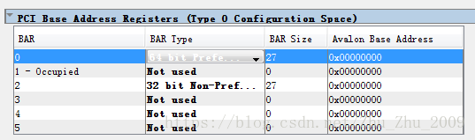
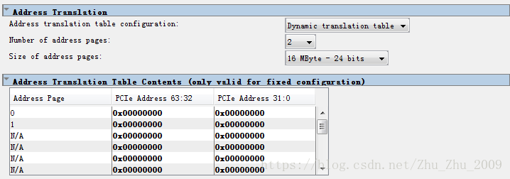
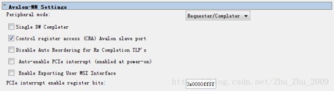
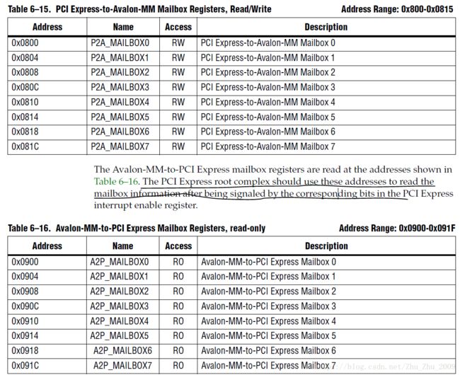
目录物理层深度剖析通道结构信号完整性关键技术链路训练(LinkTraining)协议层核心技术TLP(事务层包)结构虚拟通道管理原子操作(PCIe5.0+)硬件实现关键FPGA实现方案信号完整性设计规范总结:PCIe技术本质TeleScanPE是一个免费的PCIExpress/NVMe配置空间读/写实用程序,允许用户扫描、解码、显示和写入PCIExpress/NVMe配置空间寄存器。windows
- SPI代码详解FPGA-verilog部分(FPGA+STM32)(一)
MinJohnson
STM32FPGA/Verilogstm32fpgaspi
声明:本篇文章面向在已对SPI的四种时序有所了解的人我们采用SPI3模式以及将FPGA作从机,STM32作主机的方式讲解,在STM32控制部分采用的是半双工模式,但其实半双工与全双工区别不大,稍加修改即可本文章属于SPI的升级版,将原本的片选线CS_N再多加一根,变成spi_cs_cmd和spi_cs_data,当spi_cs_cmd拉低的时候表示传送的是命令(命令只由单片机发送),当cs_dat
- 混沌保密音频传输系统设计与评估
神经网络15044
算法大数据单片机音视频macos策略模式算法开发语言网络
混沌保密音频传输系统设计与评估摘要:本文设计并实现了一套基于混沌动力学的实时音频信号保密传输系统。系统核心采用改进型Rössler混沌系统产生密钥流,通过异或运算对音频信号进行加密/解密。详细阐述了系统架构、混沌电路实现、FPGA/微控制器平台部署方案,并制定了全面的评估指标体系(包括音频失真度、误码率、加密/解密时间、密钥空间、敏感性分析、统计特性等)。测试结果表明,该系统在保持音频质量的同时,
- FPGA基础 -- Verilog 锁存器简介
sz66cm
FPGA基础fpga开发
由浅入深地讲解Verilog中的锁存器(Latch)**,包括:什么是锁存器(定义与作用)锁存器的分类(透明锁存器vs边沿触发器)Verilog中锁存器的建模方式锁存器与触发器的区别锁存器的时序特性与设计陷阱实际应用与避免锁存器的最佳实践综合工具识别锁存器的方式与调试技巧一、什么是锁存器(Latch)?锁存器是一种电平敏感的时序逻辑单元,用于在特定控制信号(如enable或clk为高电平)时锁存输
- FPGA基础 -- Verilog 竞争/竞态(Race Condition)
一、什么是“竞争/竞态(RaceCondition)”?概念说明典型后果信号竞争(GlitchRace)由两条或多条逻辑路径传播延迟不同导致。同一时刻从不同路径到达的电平先后顺序不可预知,产生毛刺或错误翻转。硬件级:产生额外脉冲,触发错误状态或计数。事件竞争/仿真竞态(SchedulingRace)仿真器在同一个时刻deltacycle内对同一变量存在多个驱动且调度顺序不确定(典型如=阻塞赋值)。
- FPGA芯片企业需要做哪些认证?
FPGA芯片厂商,为了符合行业和客户的要求,保证产品的质量,需要在公司层面和产品层面完成一些标准的三方认证。具体需要做哪些,我做了一下整理:一:公司级认证(体系认证)不绑定具体产品:认证结果适用于企业在该体系下开发或制造的所有芯片长期有效性:认证通常有固定周期(如3年),期间无需每款芯片重复认证聚焦流程规范性:确保企业具备持续输出符合行业标准产品的能力1.1:核心质量认证(QMS)ISO9001(
- XCVU47P-2FSVH2892E Xilinx Virtex UltraScale+ FPGA AMD
XINVRY-FPGA
fpga开发fpga人工智能嵌入式硬件c++c语言阿里云
XCVU47P-2FSVH2892E是一款为超高带宽、超大逻辑、低延迟应用而生的旗舰级FPGA。它不仅为AI与网络加速提供了理想平台,也在5G与未来通信基础设施中发挥着核心作用。凭借其灵活架构、卓越性能和丰富生态。1.超大规模逻辑资源搭载约285万逻辑单元与16万多个可编程逻辑模块(ALM),适合构建超复杂的硬件算法,如AI推理引擎、大规模状态机与并行数据流处理器。2.万级DSP运算单元9,000
- FPGA基础 -- Verilog 的值变转储文件(VCD:Value Change Dump)
sz66cm
FPGA基础fpga开发
Verilog的“值变转储文件(VCD:ValueChangeDump)”,这是一项在仿真调试中至关重要的技术,可以帮助你“看见”RTL中每个信号随时间的变化过程。一、什么是Verilog的值变转储文件(VCD)VCD文件是一种标准格式的文本文件,全称为ValueChangeDump,用于记录Verilog仿真过程中信号的取值变化。它的作用类似于逻辑分析仪的抓取波形,但作用于RTL层,用于:波形观
- FPGA基础 -- Verilog 的属性(Attributes)
sz66cm
FPGA基础fpga开发
Verilog的属性(Attributes)的系统化培训内容,适用于希望深入理解属性如何在综合、仿真和工具指示中使用的专业工程师。内容将涵盖:属性的定义、语法、使用场景、典型示例、工具兼容性与注意事项。一、什么是Verilog的属性(Attribute)Verilog的属性是附加在语句或对象上的元信息(Metadata),不会改变功能行为,但用于指导综合器、仿真器或其他EDA工具的行为,例如:优化
- 在 DE2-115 开发板上使用 Chisel 编写流水灯程序
奈一410
fpga开发
在DE2-115开发板上使用Chisel编写流水灯程序步骤1:打开QuartusII软件步骤2:编写Verilog代码步骤3:配置项目步骤4:分配引脚步骤5:编译项目步骤6:下载比特流到FPGA步骤7:测试流水灯注意事项在DE2-115开发板上使用Verilog编写流水灯程序,可以遵循以下步骤:步骤1:打开QuartusII软件启动QuartusII软件并创建一个新项目,选择适合DE2-115开发
- FPGA基础 -- Verilog 共享任务(task)和函数(function)
sz66cm
FPGA基础fpga开发
Verilog中共享任务(task)和函数(function)的详细专业培训,适合具有一定RTL编程经验的工程师深入掌握。一、任务(task)与函数(function)的基本区别特性taskfunction调用方式可以在过程块中调用可以在表达式中调用返回值无返回值,通过output/inout传递必须有返回值执行周期可以包含时间延迟#、事件@不能有任何延迟并发可与fork...join结合实现并发
- 宽带中频10.4G采集卡
宽带中频10.4G采集卡同时支持交流耦合与双极性宽带信号输入的高精度高速数据采集卡,它提供12位双通道5.2GS/s或单通道10.4GA/D通道,全功率模拟带宽(-3dB)8GHz。板载FPGA具备实时信号处理能力,可以进行大数据量的实时信号处理,这些特性使其成为超宽带信号采集、雷达、复杂电磁环境及无线频谱应用领域进行信号采集和分析的理想工具。提供快速的PCIExpress3.0x8数据传输接口,
- PCIe宽带中频采集回放平台3GS/s 采集14bit 2通道 12.6GS/s回放 16bit 2通道
FPGA_ADDA
fpga开发信号处理信息与通信嵌入式硬件
PCIe宽带中频采集回放平台3GS/s采集14bit2通道12.6GS/s回放16bit2通道,是一款具备交流耦合和双极性宽带信号输入的高速数据采集卡,它具有2通道,14bit,3GS/s采集和2通道,16bit,12.6GS/s回放特性。板载FPGA具备实时信号处理能力,可实现数字下变频DDC、数字滤波、快速傅立叶变换等信号处理算法。提供快速的PCIExpress3.0x8数据传输接口,以及灵活
- 中频收发卡-采集回放
FPGA_ADDA
fpga开发FPGA加速卡KU115高速采集卡
中频收发卡是一款集成高速AD和DA转换器超高带宽PCIe总线高速采集回放板卡。它具有14bit分辨率、3GS/sAD采样率和12.6GS/sDA更新率,基于XilinxKU060FPGA系列。高速AD/DA转换器适用于雷达或通信中的高频和中频信号采集与数据回放,板载开放FPGA工程为用户开发与部署定制FPGA处理IP带来便利。提供快速的PCIExpress3.0x8数据传输接口,附带的通用IO接口
- 强大的销售团队背后 竟然是大数据分析的身影
蓝儿唯美
数据分析
Mark Roberge是HubSpot的首席财务官,在招聘销售职位时使用了大量数据分析。但是科技并没有挤走直觉。
大家都知道数理学家实际上已经渗透到了各行各业。这些热衷数据的人们通过处理数据理解商业流程的各个方面,以重组弱点,增强优势。
Mark Roberge是美国HubSpot公司的首席财务官,HubSpot公司在构架集客营销现象方面出过一份力——因此他也是一位数理学家。他使用数据分析
- Haproxy+Keepalived高可用双机单活
bylijinnan
负载均衡keepalivedhaproxy高可用
我们的应用MyApp不支持集群,但要求双机单活(两台机器:master和slave):
1.正常情况下,只有master启动MyApp并提供服务
2.当master发生故障时,slave自动启动本机的MyApp,同时虚拟IP漂移至slave,保持对外提供服务的IP和端口不变
F5据说也能满足上面的需求,但F5的通常用法都是双机双活,单活的话还没研究过
服务器资源
10.7
- eclipse编辑器中文乱码问题解决
0624chenhong
eclipse乱码
使用Eclipse编辑文件经常出现中文乱码或者文件中有中文不能保存的问题,Eclipse提供了灵活的设置文件编码格式的选项,我们可以通过设置编码 格式解决乱码问题。在Eclipse可以从几个层面设置编码格式:Workspace、Project、Content Type、File
本文以Eclipse 3.3(英文)为例加以说明:
1. 设置Workspace的编码格式:
Windows-&g
- 基础篇--resources资源
不懂事的小屁孩
android
最近一直在做java开发,偶尔敲点android代码,突然发现有些基础给忘记了,今天用半天时间温顾一下resources的资源。
String.xml 字符串资源 涉及国际化问题
http://www.2cto.com/kf/201302/190394.html
string-array
- 接上篇补上window平台自动上传证书文件的批处理问卷
酷的飞上天空
window
@echo off
: host=服务器证书域名或ip,需要和部署时服务器的域名或ip一致 ou=公司名称, o=公司名称
set host=localhost
set ou=localhost
set o=localhost
set password=123456
set validity=3650
set salias=s
- 企业物联网大潮涌动:如何做好准备?
蓝儿唯美
企业
物联网的可能性也许是无限的。要找出架构师可以做好准备的领域然后利用日益连接的世界。
尽管物联网(IoT)还很新,企业架构师现在也应该为一个连接更加紧密的未来做好计划,而不是跟上闸门被打开后的集成挑战。“问题不在于物联网正在进入哪些领域,而是哪些地方物联网没有在企业推进,” Gartner研究总监Mike Walker说。
Gartner预测到2020年物联网设备安装量将达260亿,这些设备在全
- spring学习——数据库(mybatis持久化框架配置)
a-john
mybatis
Spring提供了一组数据访问框架,集成了多种数据访问技术。无论是JDBC,iBATIS(mybatis)还是Hibernate,Spring都能够帮助消除持久化代码中单调枯燥的数据访问逻辑。可以依赖Spring来处理底层的数据访问。
mybatis是一种Spring持久化框架,要使用mybatis,就要做好相应的配置:
1,配置数据源。有很多数据源可以选择,如:DBCP,JDBC,aliba
- Java静态代理、动态代理实例
aijuans
Java静态代理
采用Java代理模式,代理类通过调用委托类对象的方法,来提供特定的服务。委托类需要实现一个业务接口,代理类返回委托类的实例接口对象。
按照代理类的创建时期,可以分为:静态代理和动态代理。
所谓静态代理: 指程序员创建好代理类,编译时直接生成代理类的字节码文件。
所谓动态代理: 在程序运行时,通过反射机制动态生成代理类。
一、静态代理类实例:
1、Serivce.ja
- Struts1与Struts2的12点区别
asia007
Struts1与Struts2
1) 在Action实现类方面的对比:Struts 1要求Action类继承一个抽象基类;Struts 1的一个具体问题是使用抽象类编程而不是接口。Struts 2 Action类可以实现一个Action接口,也可以实现其他接口,使可选和定制的服务成为可能。Struts 2提供一个ActionSupport基类去实现常用的接口。即使Action接口不是必须实现的,只有一个包含execute方法的P
- 初学者要多看看帮助文档 不要用js来写Jquery的代码
百合不是茶
jqueryjs
解析json数据的时候需要将解析的数据写到文本框中, 出现了用js来写Jquery代码的问题;
1, JQuery的赋值 有问题
代码如下: data.username 表示的是: 网易
$("#use
- 经理怎么和员工搞好关系和信任
bijian1013
团队项目管理管理
产品经理应该有坚实的专业基础,这里的基础包括产品方向和产品策略的把握,包括设计,也包括对技术的理解和见识,对运营和市场的敏感,以及良好的沟通和协作能力。换言之,既然是产品经理,整个产品的方方面面都应该能摸得出门道。这也不懂那也不懂,如何让人信服?如何让自己懂?就是不断学习,不仅仅从书本中,更从平时和各种角色的沟通
- 如何为rich:tree不同类型节点设置右键菜单
sunjing
contextMenutreeRichfaces
组合使用target和targetSelector就可以啦,如下: <rich:tree id="ruleTree" value="#{treeAction.ruleTree}" var="node" nodeType="#{node.type}"
selectionChangeListener=&qu
- 【Redis二】Redis2.8.17搭建主从复制环境
bit1129
redis
开始使用Redis2.8.17
Redis第一篇在Redis2.4.5上搭建主从复制环境,对它的主从复制的工作机制,真正的惊呆了。不知道Redis2.8.17的主从复制机制是怎样的,Redis到了2.4.5这个版本,主从复制还做成那样,Impossible is nothing! 本篇把主从复制环境再搭一遍看看效果,这次在Unbuntu上用官方支持的版本。 Ubuntu上安装Red
- JSONObject转换JSON--将Date转换为指定格式
白糖_
JSONObject
项目中,经常会用JSONObject插件将JavaBean或List<JavaBean>转换为JSON格式的字符串,而JavaBean的属性有时候会有java.util.Date这个类型的时间对象,这时JSONObject默认会将Date属性转换成这样的格式:
{"nanos":0,"time":-27076233600000,
- JavaScript语言精粹读书笔记
braveCS
JavaScript
【经典用法】:
//①定义新方法
Function .prototype.method=function(name, func){
this.prototype[name]=func;
return this;
}
//②给Object增加一个create方法,这个方法创建一个使用原对
- 编程之美-找符合条件的整数 用字符串来表示大整数避免溢出
bylijinnan
编程之美
import java.util.LinkedList;
public class FindInteger {
/**
* 编程之美 找符合条件的整数 用字符串来表示大整数避免溢出
* 题目:任意给定一个正整数N,求一个最小的正整数M(M>1),使得N*M的十进制表示形式里只含有1和0
*
* 假设当前正在搜索由0,1组成的K位十进制数
- 读书笔记
chengxuyuancsdn
读书笔记
1、Struts访问资源
2、把静态参数传递给一个动作
3、<result>type属性
4、s:iterator、s:if c:forEach
5、StringBuilder和StringBuffer
6、spring配置拦截器
1、访问资源
(1)通过ServletActionContext对象和实现ServletContextAware,ServletReque
- [通讯与电力]光网城市建设的一些问题
comsci
问题
信号防护的问题,前面已经说过了,这里要说光网交换机与市电保障的关系
我们过去用的ADSL线路,因为是电话线,在小区和街道电力中断的情况下,只要在家里用笔记本电脑+蓄电池,连接ADSL,同样可以上网........
- oracle 空间RESUMABLE
daizj
oracle空间不足RESUMABLE错误挂起
空间RESUMABLE操作 转
Oracle从9i开始引入这个功能,当出现空间不足等相关的错误时,Oracle可以不是马上返回错误信息,并回滚当前的操作,而是将操作挂起,直到挂起时间超过RESUMABLE TIMEOUT,或者空间不足的错误被解决。
这一篇简单介绍空间RESUMABLE的例子。
第一次碰到这个特性是在一次安装9i数据库的过程中,在利用D
- 重构第一次写的线程池
dieslrae
线程池 python
最近没有什么学习欲望,修改之前的线程池的计划一直搁置,这几天比较闲,还是做了一次重构,由之前的2个类拆分为现在的4个类.
1、首先是工作线程类:TaskThread,此类为一个工作线程,用于完成一个工作任务,提供等待(wait),继续(proceed),绑定任务(bindTask)等方法
#!/usr/bin/env python
# -*- coding:utf8 -*-
- C语言学习六指针
dcj3sjt126com
c
初识指针,简单示例程序:
/*
指针就是地址,地址就是指针
地址就是内存单元的编号
指针变量是存放地址的变量
指针和指针变量是两个不同的概念
但是要注意: 通常我们叙述时会把指针变量简称为指针,实际它们含义并不一样
*/
# include <stdio.h>
int main(void)
{
int * p; // p是变量的名字, int *
- yii2 beforeSave afterSave beforeDelete
dcj3sjt126com
delete
public function afterSave($insert, $changedAttributes)
{
parent::afterSave($insert, $changedAttributes);
if($insert) {
//这里是新增数据
} else {
//这里是更新数据
}
}
- timertask
shuizhaosi888
timertask
java.util.Timer timer = new java.util.Timer(true);
// true 说明这个timer以daemon方式运行(优先级低,
// 程序结束timer也自动结束),注意,javax.swing
// 包中也有一个Timer类,如果import中用到swing包,
// 要注意名字的冲突。
TimerTask task = new
- Spring Security(13)——session管理
234390216
sessionSpring Security攻击保护超时
session管理
目录
1.1 检测session超时
1.2 concurrency-control
1.3 session 固定攻击保护
- 公司项目NODEJS实践0.3[ mongo / session ...]
逐行分析JS源代码
mongodbsessionnodejs
http://www.upopen.cn
一、前言
书接上回,我们搭建了WEB服务端路由、模板等功能,完成了register 通过ajax与后端的通信,今天主要完成数据与mongodb的存取,实现注册 / 登录 /
- pojo.vo.po.domain区别
LiaoJuncai
javaVOPOJOjavabeandomain
POJO = "Plain Old Java Object",是MartinFowler等发明的一个术语,用来表示普通的Java对象,不是JavaBean, EntityBean 或者 SessionBean。POJO不但当任何特殊的角色,也不实现任何特殊的Java框架的接口如,EJB, JDBC等等。
即POJO是一个简单的普通的Java对象,它包含业务逻辑
- Windows Error Code
OhMyCC
windows
0 操作成功完成.
1 功能错误.
2 系统找不到指定的文件.
3 系统找不到指定的路径.
4 系统无法打开文件.
5 拒绝访问.
6 句柄无效.
7 存储控制块被损坏.
8 存储空间不足, 无法处理此命令.
9 存储控制块地址无效.
10 环境错误.
11 试图加载格式错误的程序.
12 访问码无效.
13 数据无效.
14 存储器不足, 无法完成此操作.
15 系
- 在storm集群环境下发布Topology
roadrunners
集群stormtopologyspoutbolt
storm的topology设计和开发就略过了。本章主要来说说如何在storm的集群环境中,通过storm的管理命令来发布和管理集群中的topology。
1、打包
打包插件是使用maven提供的maven-shade-plugin,详细见maven-shade-plugin。
<plugin>
<groupId>org.apache.maven.
- 为什么不允许代码里出现“魔数”
tomcat_oracle
java
在一个新项目中,我最先做的事情之一,就是建立使用诸如Checkstyle和Findbugs之类工具的准则。目的是制定一些代码规范,以及避免通过静态代码分析就能够检测到的bug。 迟早会有人给出案例说这样太离谱了。其中的一个案例是Checkstyle的魔数检查。它会对任何没有定义常量就使用的数字字面量给出警告,除了-1、0、1和2。 很多开发者在这个检查方面都有问题,这可以从结果
- zoj 3511 Cake Robbery(线段树)
阿尔萨斯
线段树
题目链接:zoj 3511 Cake Robbery
题目大意:就是有一个N边形的蛋糕,切M刀,从中挑选一块边数最多的,保证没有两条边重叠。
解题思路:有多少个顶点即为有多少条边,所以直接按照切刀切掉点的个数排序,然后用线段树维护剩下的还有哪些点。
#include <cstdio>
#include <cstring>
#include <vector&