用NMOS搭建自动双向电平转换电路
以下内容摘自“AN97055”
2.3 Devices with different logic levels connected via the bi-directional level shifter.
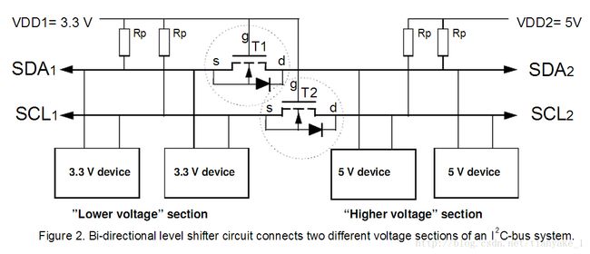
The bi-directional level shifter is used to interconnect two sections of an I2C-bus system, each section with adifferent supply voltage and different logic levels. In the bus system of Figure 2 the left section has pull-up resistors and devices connected to a 3.3 Volt supply voltage, the right section has pull-up resistors and devicesconnected to a 5 Volt supply voltage. The devices of each section have I/O’s with supply voltage related logicinput levels and an open drain output configuration.

The level shifter for each bus line is identical and consists of one discrete N-channel enhancement MOS-FET, T1 for the serial data line SDA and T2 for the serial clock line SCL. The gates (g) has to be connected to thelowest supply voltage VDD1 , the sources (s) to the bus lines of the “Lower voltage” section, and the drains (d)to the bus lines of the “Higher voltage” section. Many MOS-FET’s have the substrate internally alreadyconnected with its source, otherwise it should be done externally. The diode between the drain (d) andsubstrate is inside the MOS-FET present as n-p junction of drain and substrate.
2.3.1 Description of the level shift operation.
For the level shift operation three states has to be considered:
• State 1.
No device is pulling down the bus line and the bus line of the “Lower voltage” section is pulled upby its pull-up resistors Rp to 3.3 V. The gate and the source of the MOS-FET are both at 3.3 V, so its VGS is below the threshold voltage and the MOS-FET is not conducting. This allows that the bus line at the“Higher voltage” section is pulled up by its pull-up resistor Rp to 5V. So the bus lines of both sections areHIGH, but at a different voltage level.
•State 2.
A 3.3 V device pulls down the bus line to a LOW level. The source of the MOS-FET becomesalso LOW, while the gate stay at 3.3 V. The VGS rises above the threshold and the MOS-FET becomesconducting. Now the bus line of the “Higher voltage” section is also pulled down to a LOW level by the 3.3V device via the conducting MOS-FET. So the bus lines of both sections become LOW at the samevoltage level.
• State 3.
A 5 V device pulls down the bus line to a LOW level. Via the drain-substrate diode of the MOS-FET the “Lower voltage” section is in first instance pulled down until VGS passes the threshold and theMOS-FET becomes conducting. Now the bus line of the “Lower voltage” section is further pulled down toa LOW level by the 5 V device via the conducting MOS-FET. So the bus lines of both sections becomeLOW at the same voltage level.
The three states show that the logic levels are transferred in both directions of the bus system, independent ofthe driving section. State 2 and state 3 perform the “wired AND” function between the bus lines of both sections as required by the I2C-bus specification.
Other supply voltages than 3.3V for VDD1 and 5V for VDD2 can be applied, e.g. 2V for VDD1 and 10V forVDD2 is feasible. In normal operation VDD2 must be equal to or higher than VDD1.
The MOS-FET’s allow that VDD2 is lower than VDD1 during switching power on/off, of course the bus systemis not operational during that time.
The maximum VDD2 is not critical as long as the drain of the MOS-FET can withstand this voltage. At a higher VDD2 a slower falling edge for both bus sections has to be taken in account, both in state 2 and state 3,because it takes more discharge time of the bus line.
The lowest possible supply voltage VDD1 depends on the threshold voltage VGS(th) of the MOS-FET’s. With athreshold voltage of about 1 Volt below the lowest VDD1, the level shifter circuit will operate properly. If forexample the lowest VDD1 is 3 Volt, a threshold voltage VGS(th) of maximum 2 Volt is allowed.
2.3.5 Extended circuit for isolation of the powered-down“higher voltage”section.
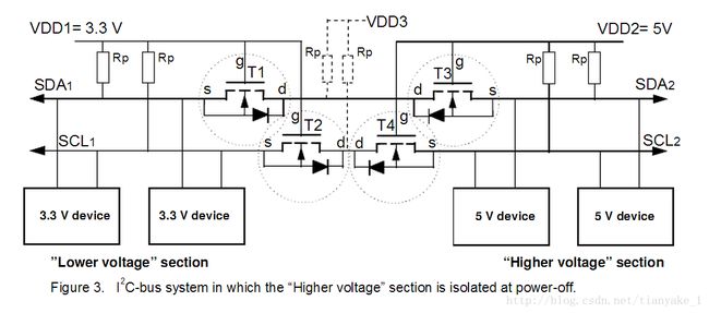
If it is necessary to isolate also the “Higher voltage” section when it is powered off, then the level shifter circuitcan be extended as shown in figure 3.

If VDD2 is switched-off then T3 and T4 becomes not conducting and the “Higher voltage” section is isolatedfrom the other part of the bus system. The pull-up resistors Rp to VDD3 are not necessary for the properoperation and may have a high resistance value, they can be added to prevent the MOS-FET drains becomefloating at a HIGH level. VDD3 is preferably connected to the highest supply voltage. If VDD3 has a lowervalue, then care must be taken that the logic HIGH levels of the bus lines are not decreased too much.The “Lower voltage” section is isolated if VDD1 is switched off, in the same way as in Figure 2 and described in2.3.4, but now independent of the value of VDD2.
Because this level shifter circuit is symmetrical, the “Lower voltage” section and “Higher voltage” section can bechosen arbitrary at the left or right side in figure 3. Even more sections with a higher, a lower or a same supplyvoltage value can be added by connecting these sections via additional MOS-FET’s to the common drainterminals (d) in the same way as the other sections in Figure 3. Every section is isolated from the rest of thebus system when its supply voltage is switched off, while level shifting between all other sections remainoperational.
3. CHARACTERISTICS OF THE MOS-FET’S.
The requirements for the most important characteristics of the MOS-FET’s, used as bi-directional level shifter in an I2C-bus system with max. 6V and min. 2.7V levels, are listed below. The values are intended as an indicationand may be adapted for other supply voltages, other logic levels and/or other applications.

Values of pull-up resistors and series resistors are not given here, they depend on the worst case values of thesupply voltages and logic levels, length and load of the bus lines, and the requirements for rise and fall times.These resistors have to be calculated for each bus system separately. A good approach for the calculation is tokeep the RC values for the different sections about the same, it gives the best timing tolerances for set-up andhold times.
MOS-FET’s in table 1 are suitable to be used as level shifter. See Philips Data Handbook SC07 for their fullspecification. BSN10 or BSN20 are low cost devices and have good properties for 3V/5V level shifting, isolationand protection.
