DRAM的结构原理剖析
文字参考:
https://www.cnblogs.com/yilang/p/11103061.html
https://www.techbang.com/posts/18381-from-the-channel-to-address-computer-main-memory-structures-to-understand
http://lackingrhoticity.blogspot.com/2015/05/how-physical-addresses-map-to-rows-and-banks.html
视频学习详情参见:
https://www.bilibili.com/video/BV19b411i784?p=49
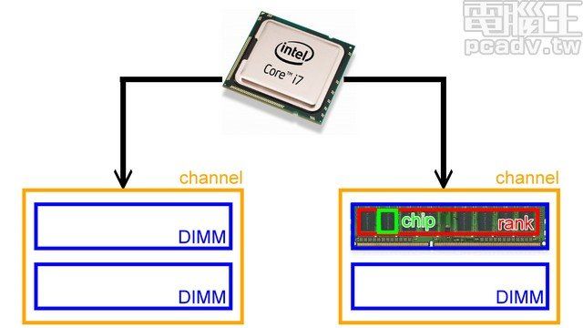
一、DRAM的存储结构
channel>DIMM>rank>chip>bank>Memory Array>row/column
1、channel 和 DIMM,DIMM和RANK
SIMM----->DIMM
2、rank 和 chip

现在市场上的DIMM条一般都有2个RANK。rank 指的是连接到同 一个CS(Chip Select)的chip,内存控制器能对同 一 rank 的 chip 进行读写操作。
Rank
CPU与内存之间的接口位宽是64bit,也就意味着CPU在一个时钟周期内会向内存发送或从内存读取64bit的数据。可是,单个内存颗粒的位宽仅有4bit、8bit或16bit,个别也有32bit的。因此,必须把多个颗粒并联起来,组成一个位宽为64bit的数据集合,才可以和CPU互连。生产商把64bit集合称为一个物理BANK(Physical BANK),简写为P-BANK。为了和逻辑BANK相区分,也经常把P-BANK称为RANK或Physical RANK,把L-BANK则简称为BANK。如果每个内存颗粒的位宽是8bit,应该由8个颗粒并联起来,组成一个RANK(64bit);同理,如果颗粒的位宽是16bit,应该由4个颗粒组成一个RANK。由此可知:Rank其实就是一组内存颗粒位宽的集合,也可以叫Chips,在PCB上,往往把一面上的内存颗粒组成一个Rank,另一面是另外一个Rank(假若有的话),这样也可以将Rank理解内存条的Side(面)。具体说,当颗粒位宽×颗粒 数=64bits时,这个模组就是有一个RANK。为了保证和CPU的沟通,一个模组至少要有一个RANK。但是,为了保证有一定的内存容量,目前,DDR2内存,经常是采用一个模组两个RANK的架构。“模组构成”中的“R”“RANK”的意思。“2R”是说组成模组的RANK数(Number of ranks of memory installed)是2个。有“1R”和“2R”两种;“模组构成”中的“×8”是颗粒的位宽(bit width),有×4、×8和×16三种.
Chip(Memory)
存储芯片,又叫内存颗粒。真正提供存储的器件。
3、chip 和 bank
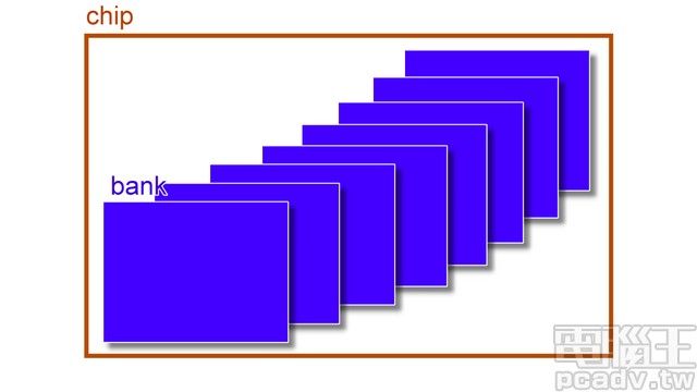
chip 往下拆分為 bank,如图所示,一个chip有8个bank。
4、bank 和 memory array
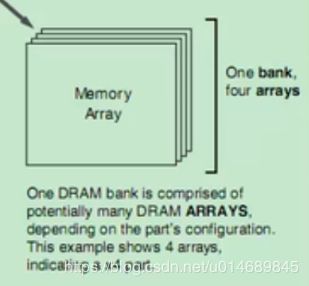
一个Bank包含多个memory arrays,比如4个、8个或者16个,这个memory arrays的数量也代表个一个chip的数据位宽。我们日常接触到的三星的8Gb 的DDR4颗粒的数据位宽就是8bit,说明这个颗粒(chip)的一个bank有8个arrays。
5、memory array和row/column

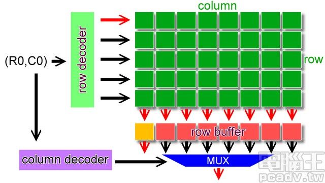
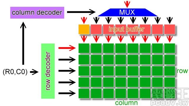
memory array往下拆就是 1 個個的儲存單元,橫向 1 排稱之為 row,直向 1 排稱之為 column,每排 column 的下方都有個 row buffer,用以暫存讀出來的 row 排資料。
一般來說橫向選擇排數的線路稱為 row(row enable、row select、word line),直向負責傳遞訊號的線路為column(bitline),每組 bank 的下方還會有個 row buffer(sense amplifier),負責將獨出的 row 資料暫存,等待 column 位址送到後輸出正確的位元,以及判斷儲存的逻辑值是 0 還是 1。
二、内存的读写
内存控制器和DIMM之间的线路连接如下:
一个bank的读操作如下:
一个bank的写操作如下:
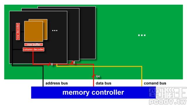
读操作时,首先内存控制器會將 1 組地址由位址線傳到内存上,控制線跟著傳送控制訊號;如果是多 rank 的安裝情形,CS 也會送出對應的訊號選擇目標 rank。接著由於每個 rank 由許多 chip 組成,1 個 chip 僅負責部分的資料讀取,chip 接收到位址訊號後,將位址丟入內部的 row/column 解碼器找出相對應的 bank 位址(每家每款產品的內部 bank 組合有可能不同,因此對應也會有所不同),接著開啟 row 線,同 1 排 row 的內部資料就會流到 row buffer 內部,row buffer 判斷訊號為 0 或是 1 之後就輸出資料。
写操作时,除了地址数据外,还会传送欲写入的数据至晶片內部的 input buffer,同樣的也是依照 row/column 解碼器找出對應位置之后再写入。

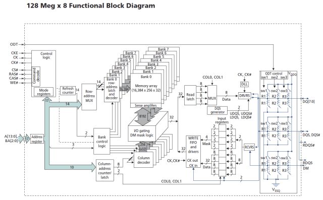
一个DRAM 晶片的内部功能图如下所示:
三、How physical addresses map to rows and banks in DRAM
参考:http://lackingrhoticity.blogspot.com/2015/05/how-physical-addresses-map-to-rows-and-banks.html
Now I'll discuss how these CPUs' memory controllers map physical addresses to locations in DRAM -- specifically, to row, bank and column numbers in DRAM modules. Let's call this the DRAM address mapping. I'll use one test machine as a case study.
Motivation: the rowhammer bug
I am interested in the DRAM address mapping because it is relevant to the "rowhammer" bug.
Rowhammer is a problem with some DRAM modules whereby certain pessimal memory access patterns can cause memory corruption. In these DRAMs, repeatedly activating a row of memory (termed "row hammering") can produce electrical disturbances that produce bit flips in vulnerable cells in adjacent rows of memory.
These repeated row activations can be caused by repeatedly accessing a pair of DRAM locations that are in different rows of the same bank of DRAM. Knowing the DRAM address mapping is useful because it tells us which pairs of addresses satisfy this "same bank, different row" (SBDR) property.
Guessing and checking an address mapping
For my case study, I have a test machine containing DRAM that is vulnerable to the rowhammer problem. Running rowhammer_test on this machine demonstrates bit flips.
I'd like to know what the DRAM address mapping is for this machine, but apparently it isn't publicly documented: This machine has a Sandy Bridge CPU, but Intel don't document the address mapping used by these CPUs' memory controllers.
rowhammer_test does not actually need to identify SBDR address pairs.rowhammer_test just repeatedly tries hammering randomly chosen address pairs. Typically 1/8 or 1/16 of these pairs will be SBDR pairs, because our machine has 8 banks per DIMM (and 16 banks in total). So, while we don't need to know the DRAM address mapping to cause bit flips on this machine, knowing it would help us be more targeted in our testing.
Though the address mapping isn't documented, I found that I can make an educated guess at what the mapping is, based on the DRAM's geometry, and then verify the guess based on the physical addresses that rowhammer_test reports. rowhammer_test can report the physical addresses where bit flips occur ("victims") and the pairs of physical addresses that produce those bit flips ("aggressors"). Since these pairs must be SBDR pairs, we can check a hypothesised address mapping against this empirical data.
Memory geometry
The first step in hypothesising an address mapping for a machine is to check how many DIMMs the machine has and how these DIMMs are organised internally.
I can query information about the DIMMs using the decode-dimms tool on Linux. (In Ubuntu, decode-dimms is in the i2c-tools package.) This tool decodes the DIMMs' SPD (Serial Presence Detect) metadata.
My test machine has 2 * 4GB SO-DIMMs, giving 8GB of memory in total.
decode-dimms reports the following information for both of the DIMMs:
Size                                            4096 MB
Banks x Rows x Columns x Bits                   8 x 15 x 10 x 64
Ranks                                           2
This means that, for each DIMM:
- Each of the DIMM's banks contains 2^15 rows (32768 rows).
- Each row contains 2^10 * 64 bits = 2^16 bits = 2^13 bytes = 8 kbytes.
Each DIMM has 2 ranks and 8 banks. Cross checking the capacity of the DIMM gives us the reported size, as expected:
8 kbytes per row * 32768 rows * 2 ranks * 8 banks = 4096 MB = 4 GB
The DRAM address mapping
On my test machine, it appears that the bits of physical addresses are used as follows:
- Bits 0-5: These are the lower 6 bits of the byte index within a row (i.e. the 6-bit index into a 64-byte cache line).
- Bit 6: This is a 1-bit channel number, which selects between the 2 DIMMs.
- Bits 7-13: These are the upper 7 bits of the index within a row (i.e. the upper bits of the column number).
- Bits 14-16: These are XOR'd with the bottom 3 bits of the row number to give the 3-bit bank number.
- Bit 17: This is a 1-bit rank number, which selects between the 2 ranks of a DIMM (which are typically the two sides of the DIMM's circuit board).
- Bits 18-32: These are the 15-bit row number.
- Bits 33+: These may be set because physical memory starts at physical addresses greater than 0.
Why is the mapping like that?
This mapping fits the results from rowhammer_test (see below), but we can also explain that the address bits are mapped this way to give good performance for typical memory access patterns, such as sequential accesses and strided accesses:
-
Channel parallelism: Placing the channel number at bit 6 means that cache lines will alternate between the two channels (i.e. the two DIMMs), which can be accessed in parallel. This means that if we're accessing addresses sequentially, the load will be spread across the two channels.
As an aside, Ivy Bridge (the successor to Sandy Bridge) apparently makes the mapping of the channel number more complex. An Intel presentation mentions "Channel hashing" and says that this "Allows channel selection to be made based on multiple address bits. Historically, it had been "A[6]". Allows more even distribution of memory accesses across channels."
-
Bank thrashing: Generally, column, bank and row numbers are arranged to minimise "bank thrashing" (frequently changing a bank's currently activated row).
Some background: DRAM modules are organised into banks, which in turn are organised into rows. Each bank has a "currently activated row" whose contents are copied into a row buffer which acts as a cache that can be accessed quickly. Accessing a different row takes longer because that row must be activated first. So, the DRAM address mapping places SBDR pairs as far apart as possible in physical address space.
Row hammering is a special case of bank thrashing where two particular rows are repeatedly activated (perhaps deliberately).
-
Bank parallelism: Banks can be accessed in parallel (though to a lesser degree than channels), so the bank number changes before the row number as the address is increased.
-
XOR scheme: XORing the row number's lower bits into the bank number is a trick to avoid bank thrashing when accessing arrays with large strides. For example, in the mapping above, the XORing causes addresses X and X+256k to be placed in different banks instead of being an SBDR pair.
Bank/row XORing schemes are described in various places, such as:
- David Tawei Wang's PhD thesis, "Modern DRAM memory systems: Performance analysis and scheduling algorithms", 2005. See section 5.3.5, "Bank Address Aliasing (stride collision)". This thesis has some good background info on DRAM in general.
- The paper "Reducing DRAM Latencies with an Integrated Memory Hierarchy Design", 2001. See Figure 3.
Checking against rowhammer_test's output
I ran rowhammer_test_ext (the extended version of rowhammer_test) on my test machine for 6 hours, and it found repeatable bit flips at 22 locations. (See the raw data and analysis code.)
The row hammering test generates a set of (A1, A2, V) triples, where:
- V is the victim address where we see the bit flip.
- A1 and A2 are the aggressor addresses that we hammer.
- We sort A1 and A2 so that A1 is closer to V than A2 is. We tentatively assume that the closer address, A1, is the one that actually causes the bit flips (though this wouldn't necessarily be true if the DRAM address mapping were more complicated).
There are three properties we expect to hold for all of these results:
-
Row: A1 and V's row numbers should differ by 1 -- i.e. they should be in adjacent rows. (A2 can have any row number.)
This property makes it easy to work out where the bottom bits of the row number are in the physical address.
We find this property holds for all but 2 of the results. In those 2 results, the row numbers differ by 3 rather than 1.
-
Bank: V, A1 and A2 should have the same bank number. Indeed, we find this property holds for all 22 results. This only holds when applying the row/bank XORing scheme.
-
Channel: V, A1 and A2 should have the same channel number. This holds for all the results. It happens that all of our results have channel=0, because rowhammer_test only selects 4k-aligned addresses and so only tests one channel. (Maybe this could be considered a bug.)
Possible further testing
There are two further experiments we could run to check whether the DRAM address mapping evaluates the SBDR property correctly, which I haven't tried yet:
-
Timing tests: Accessing SBDR address pairs repeatedly should be slower than accessing non-SBDR pairs repeatedly, because the former cause row activations and the latter don't.
-
Exhaustive rowhammer testing: Once we've found an aggressor address, A1, that causes a repeatable bit flip, we can test this against many values of address A2. Hammering (A1, A2) can produce bit flips only if this is an SBDR pair.
Furthermore, taking out one DIMM from our test machine should remove the channel bit from the DRAM address mapping and change the aggressor/victim addresses accordingly. We could check whether this is the case.