低功耗,高性能转换芯片NCS8801S:RGB/LVDS转EDP
1 Features
Embedded-DisplayPort (eDP) Output
1/2/4lane eDP @ 1.62/2.7Gbps per lane
UP to WQXGA (2560*1600) supported
Up to 6dB pre-emphasis
RGB Input
18/24bit RGB Interface
Pixel clock up to 270MHz
SDR/DDR supported
Pin order reversal supported
LVDS Input
Single/Dual-channel 6/8bit LVDS interface
400Mbps to 1Gbps per data pair
Built-in termination
Channel and polarity swap supported
Reference Clock
Any freq. between 19MHz and 100MHz
Crystal or single-ended clock input
Built-in 5000ppm SSC generator
Misc
I2C/SPI for chip configuration
Built-in eDP handshake protocol
I2C-AUX channel for TCON/DPCD/EDID
control
Built-in video test pattern
Power
1.2V core supply
2.5V or 3.3V IO supply
RGB IO can go down to 1.8V
Power consumption ~ 187mW
@ 1920*1080*24bit*60Hz, LVDS mode
Deep-sleep mode power <1mW
Package
QFN-56 (7mm x 7mm) package
RoHS Compliant
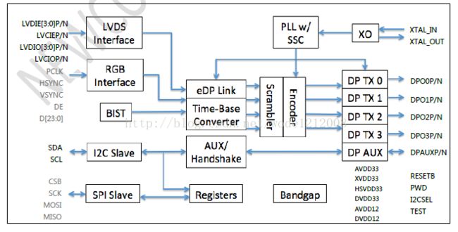
Block Diagram
3 General Description
NCS8801S is a low-power RGB/LVDS-to-DisplayPort/eDP converter, which is designed for mobile devices including smartphones, tablets, laptops, etc. to support high-definition DP/eDP displays.
NCS8801S supports 4-lane DP/eDP output which is typically required to support QXGA (2048*1536) and above at 60Hz frame rate.
All the functions including both RGB and LVDS interfaces pack into a small 7mm*7mm QFN56 package which saves the precious space in mobile devices.
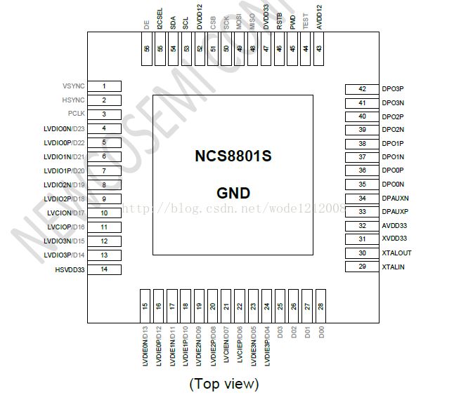
4 Pin Diagram
NCS8801S is fully compliant with NCS8801.
5 Pin Description
...
6 Electrical Specifications
...
7 Register Table
...
8 Applications
...
8.2 PCB Layout Rules
a. Due to the high data rate of the eDP signal, characteristic impedance throughout the signal path needs to be well controlled. It is highly suggested to control the differential characteristic impedance of the PCB trace to be within 100ohm±10%. Low speed connectors are highly suggested to be avoided in the eDP signal path, especially in the 2.7Gbps mode.
b. The requirement on the LVDS side is less stringent but impedance discontinuities including Y-branching are highly suggested to be minimized.
c. The crosstalk and length of the RGB traces needs to be minimized.
d. The intra-pair mismatch in all differential pairs needs to be avoided.
e. eDP inter-lane skew is suggested to be controlled under 50mil.
f. LVDS inter-lane skew is suggested to be controlled under 100mil.
g. RGB inter-line skew is suggested to be controlled under 300mil.
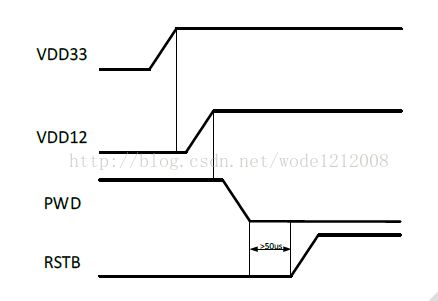
8.3 Power-on Sequence
8.4 Typical Initialization Procedure
(I2C first device ID of the chip is 0x70, write to address 0xE0, read from address 0xE1; I2C second device ID of the chip is 0x75, write to address 0xEA, read from address 0xEB).
a. Configure register 0x0f of device ID 0x70 to 0x01, to enter internal logic reset status
b. Configure register 0x00 of device ID 0x70 to choose between RGB and LVDS RX modes
c. Configure register 0x02 of device ID 0x70 to 0x07, to enable RX/TX panel parameter adaptive
d. Configure register 0x07 of device ID 0x70, to choose eDP parameter, including lane numbers, RBR/HBR, etc.
e. Configure register 0x00 of device ID 0x75 to 0xB0, to enter internal analog reset status
f. Configure register 0x0e and 0x0f of device ID0x75 to 0x10, to configure TX amplitude
g. Configure register 0x00 of device ID 0x75 to 0xB1 if the lane rate is HBR
h. Configure register 0x0f of device ID 0x70 to 0x00, to enter normal status
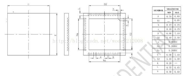
9 Package
NCS8801S is packaged in 7mm*7mm 56-pin QFN, QFN56L (0707*0.75-0.40). The package dimensions are shown below. (Unit: mm)


