exynos4412 时钟系统分析
exynos 4412 时钟域

CPU_BLK:内含Cortex-A9 MPCore处理器、L2 cache控制器、CoreSight(调试用)。CMU_CPU用于给这些部件产生时钟。
DMC_BLK:内含DRAM内存控制器(DMC)、安全子系统(Security sub system)、通用中断控制器(Generic Interrupt Controller,GIC)。CMU_DMC用于给这些部件产生时钟。
LEFTBUS_BLK和RIGHTBUS_BLK:它们是全局的数据总线,用于在DRAM和其他子模块之间传输数据。它还包含时钟频率为100MHz的全局外设总线。您可以使用100MHz时钟进行寄存器访问。
CMU_TOP:为剩余的功能块生成时钟,包括G3D,MFC,LCD0,ISP,CAM,TV,FSYS,MFC,GPS,MAUDIO,PERIL和PERIR。它产生的总线时钟工作在400/200/160/133/100MHz频率。它还生成各种特殊时钟来操作Exynos 4412芯片中的IP。
4412有4个PLL :APLL 、MPLL 、EPLL 和 VPLL ;2个 PHY :USB PHY 和 HDMI PHY (PHY:物理层, 一般指与外部信号接口的芯片 ):
① APLL:用于 CPU_BLK ;作为 MPLL 的补充,它也可以给 DMC_BLK 、LEFTBUS_BLK 、RIGHTBUS_BLK 和 CMU_TOP 提供时钟。
② MPLL:用于DMC_BLK 、LEFTBUS_BLK 、RIGHTBUS_BLK 和 CMU_TOP
③ EPLL :主要给音频模块提供时钟
④ VPLL :主要给视频系统提供54MHz时钟, 给 G3D(3D图形加速器 )提供时钟。
⑤ USB PHY :给 USB 子系统提供 30MHz 和 48MHz 时钟 。
⑥ HDMI PHY :产生 54MHz 时钟 。
MUX、PLL、DIV:
① MUX:多路复用,即从多个输入源中选择一个
② PLL:把低频率的输入时钟提高后输出
③ DIV:分频器,把高频率的输入时钟降频后输出
4412功能模块操作频率:
 时钟源的选择,三部分构成:
RTCXTI :输入源为32.768 KHz晶振,作为RTC的时钟源。
XXTI :如果没有USB Phy的话, XXTI作为CMU,APLL、MPLL、VPLL、EPLL的时钟源。输入源为12MHz~50MHz晶振
XUSBXTI :建议24MHz晶振,提供USB Phy时钟和iROM时钟源,以及各路PLL时钟源
在4412的电路原理图中找到时钟相关的电路:

从上图可以看出,XXXTI 接地,XRTCXTI接3.768K晶振,XUSBXTI接24M晶振。
下面列举clock_init_tiny4412.S中时钟初始化代码所要操作的相关寄存器:
设置CMU_CPU时钟源
CLK_SRC_CPU·
Base Address: 0x1004_0000·
Address = Base Address + 0x4200, Reset Value = 0x0000_0000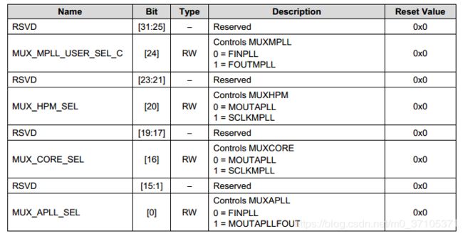
设置DMU_DMC分频
CLK_DIV_DMC0·
Base Address: 0x1004_0000·
Address = Base Address + 0x0500, Reset Value = 0x0000_0000

CLK_DIV_DMC1·
Base Address: 0x1004_0000·
Address = Base Address + 0x0504, Reset Value = 0x0000_1000

设置CMU_TOP时钟源
CLK_SRC_TOP0
Base Address: 0x1003_0000
·Address = Base Address + 0xC210, Reset Value = 0x0000_0000

CLK_SRC_TOP1
Base Address: 0x1003_0000
Address = Base Address + 0xC214, Reset Value = 0x0000_0000

设置LEFTBUS 时钟源和DIV
CLK_SRC_LEFTBUS
Base Address: 0x1003_0000
Address = Base Address + 0x4200, Reset Value = 0x0000_0000

CLK_DIV_LEFTBUS
Base Address: 0x1003_0000
Address = Base Address + 0x4500, Reset Value = 0x0000_0000 
设置RIGHTBUS 时钟源和DIV
CLK_SRC_RIGHTBUS
Base Address: 0x1003_0000
Address = Base Address + 0x8200, Reset Value = 0x0000_0000

CLK_DIV_RIGHTBUS
Base Address: 0x1003_0000
Address = Base Address + 0x8500, Reset Value = 0x0000_0000
设置PLL的一般流程如下:·
设置PLL的P、M、S值,这是根据期望得到的频率用公式计算出来的;
设置PLL的其他控制参数;
使能PLL;
PLL会等待一段时间使得时钟稳定;
设置MUX,选择PLL所输出的时钟。
设置PLL的locktime
APLL_LOCK
Base Address: 0x1004_0000
Address = Base Address + 0x4000, Reset Value = 0x0000_0FFF

MPLL_LOCK
Base Address: 0x1004_0000
Address = Base Address + 0x0008, Reset Value = 0x0000_0FFF

EPLL_LOCK
Base Address: 0x1003_0000
Address = Base Address + 0xC010, Reset Value = 0x0000_0FFF

VPLL_LOCK
Base Address: 0x1003_0000
Address = Base Address + 0xC020, Reset Value = 0x0000_0FFF

设置CMU_CPU DIV
CLK_DIV_CPU0
Base Address: 0x1004_0000
Address = Base Address + 0x4500, Reset Value = 0x0000_0000

CLK_DIV_CPU1
Base Address: 0x1004_0000
Address = Base Address + 0x4504, Reset Value = 0x0000_0000

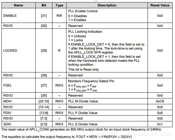
设置APLLCON寄存器
APLL_CON1
Base Address: 0x1004_0000
Address = Base Address + 0x4104, Reset Value = 0x0080_3800

APLL_CON0
Base Address: 0x1004_0000
Address = Base Address + 0x4100, Reset Value = 0x0064_0300
设置MPLLCON
MPLL_CON1
Base Address: 0x1004_0000
Address = Base Address + 0x010C, Reset Value = 0x0080_3800
MPLL_CON0
Base Address: 0x1004_0000
Address = Base Address + 0x0108, Reset Value = 0x0064_0300

4412 datasheet推荐的MPS值:

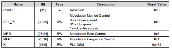
设置EPLL_CON寄存器
EPLL_CON2
Base Address: 0x1003_0000
Address = Base Address + 0xC118, Reset Value = 0x0000_0080
EPLL_CON1
Base Address: 0x1003_0000
Address = Base Address + 0xC114, Reset Value = 0x6601_0000

EPLL_CON0
Base Address: 0x1003_0000
Address = Base Address + 0xC110, Reset Value = 0x0060_0302

设置VPLL_CON寄存器
VPLL_CON2
Base Address: 0x1003_0000
Address = Base Address + 0xC128, Reset Value = 0x0000_0080
VPLL_CON1
Base Address: 0x1003_0000
Address = Base Address + 0xC124, Reset Value = 0x6601_6000
VPLL_CON0
Base Address: 0x1003_0000
Address = Base Address + 0xC120, Reset Value = 0x006F_0302

设置CMU_DMC时钟源
CLK_SRC_DMC
Base Address: 0x1004_0000
Address = Base Address + 0x0200, Reset Value = 0x0001_0000

分析clock_init_tiny4412.S的代码,涉及到相关的寄存器从上文中查看:
 system_clock_init:
 	push	{lr} /*lr入栈*/
 	ldr	r0, =ELFIN_CLOCK_BASE	/*0x1003_0000 CMU base*/
 	@ CMU_CPU MUX / DIV
 	ldr	r1, =0x0
 /	ldr	r2, =CLK_SRC_CPU_OFFSET	/*0x14200 CLK_SRC_CPU*/
 	str	r1, [r0, r2] /*设置CLK_SRC_CPU寄存器值为0x0000 0000*/

 	/* wait ?us 延时等待*/
 	mov	r1, #0x10000
 1:	subs	r1, r1, #1
 	bne	1b

	ldr	r1, =CLK_DIV_DMC0_VAL	/* 0x0 0x0 0x1<<20 | 0x1<<16 | 0x1<<12 | 0x1<<8 | 0x1<<4 | 0x3*/
	ldr	r2, =CLK_DIV_DMC0_OFFSET /*0x10500  CLK_DIV_DMC0*/
	str	r1, [r0, r2]			/*设置CLK_DIV_DMC0的值*/

	ldr	r1, =CLK_DIV_DMC1_VAL 		/*0x07071713*/
	ldr	r2, =CLK_DIV_DMC1_OFFSET	/*0x10504 CLK_DIV_DMC1*/
	str	r1, [r0, r2] 				/*设置CLK_DIV_DMC1的值*/

	@ CMU_TOP MUX / DIV
	ldr	r1, =CLK_SRC_TOP0_VAL /*0x0 0x0 0x0 0x0 0x1 0x1*/
	ldr	r2, =CLK_SRC_TOP0_OFFSET /*0x0C210 CLK_SRC_TOP0*/
	str	r1, [r0, r2]			/*设置CLK_SRC_TOP0的值*/

	ldr	r1, =CLK_SRC_TOP1_VAL /*0x01111000*/
	ldr	r2, =CLK_SRC_TOP1_OFFSET /*0x0C214 CLK_SRC_TOP1*/
	str	r1, [r0, r2] 			/*设置CLK_SRC_TOP1的值*/

	/* wait ?us */
	mov	r1, #0x10000
3:	subs	r1, r1, #1
	bne	3b

	ldr	r1, =CLK_DIV_TOP_VAL /*0x1 0x2 0x0 0x5 0x4 0x7 0x3*/
	ldr	r2, =CLK_DIV_TOP_OFFSET /*0x0C510 CLK_DIV_TOP*/
	str	r1, [r0, r2] 			/*设置CLK_DIV_TOP的值*/

	@ CMU_LEFTBUS MUX / DIV
	ldr	r1, =CLK_SRC_LEFTBUS*_VAL	/*0x10*/
	ldr	r2, =CLK_SRC_LEFTBUS_OFFSET /*CLK_SRC_LEFTBUS 0x04200*/
	str	r1, [r0, r2] 				/*设置CLK_SRC_LEFTBUS的值*/

	/* wait ?us */
	mov	r1, #0x10000
4:	subs	r1, r1, #1
	bne	4b

	ldr	r1, =CLK_DIV_LEFRBUS_VAL 	/*0x1<<4 | 0x3*/
	ldr	r2, =CLK_DIV_LEFTBUS_OFFSET	/*0x4500 CLK_DIV_LEFTBUS*/
	str	r1, [r0, r2] 				/*设置CLK_DIV_LEFTBUS的值*/

	@ CMU_RIGxTBUS MUX / DIV
	ldr	r1, =CLK_SRC_RIGHTBUS_VAL	/*0x10*/
	ldr	r2, =CLK_SRC_RIGHTBUS_OFFSET	/*0x08200 CLK_SRC_RIGHTBUS*/
	str	r1, [r0, r2] 				/*设置CLK_SRC_RIGHTBUS的值*/

	/* wait ?us */
	mov	r1, #0x10000
5:	subs	r1, r1, #1
	bne	5b

	ldr	r1, =CLK_DIV_RIGHTBUS_VAL		/*0x1<<4 | 0x3*/
	ldr	r2, =CLK_DIV_RIGHTBUS_OFFSET	/*0x08500 CLK_DIV_RIGHTBUS*/
	str	r1, [r0, r2] 				/*设置CLK_DIV_RIGHTBUS*/

	@ Set PLL locktime
	ldr	r1, =APLL_LOCK_VAL	/*APLL_PDIV * 270*/
	ldr	r2, =APLL_LOCK_OFFSET /*APLL_LOCK 0x14000*/
	str	r1, [r0, r2] 		/*设置APLL_LOCK*/

	ldr	r1, =MPLL_LOCK_VAL	/*MPLL_PDIV * 270*/
	ldr	r2, =MPLL_LOCK_OFFSET	/*MPLL_LOCK 0x14008*/
	str	r1, [r0, r2]			/*设置MPLL_LOCK*/

	ldr	r1, =EPLL_LOCK_VAL	/*EPLL_PDIV * 3000*/
	ldr	r2, =EPLL_LOCK_OFFSET	/*EPLL_LOCK 0x0C010*/
	str	r1, [r0, r2] 			/*设置EPLL_LOCK*/

	ldr	r1, =VPLL_LOCK_VAL		/*VPLL_PDIV * 3000*/
	ldr	r2, =VPLL_LOCK_OFFSET	/*VPLL_LOCK 0x0C020*/
	str	r1, [r0, r2] 			/*设置VPLL_LOCK*/

	@ Set CLK_DIV_CPU
	ldr	r1, =CLK_DIV_CPU0_VAL		/*0x0 0X2 0X1 0X6 0X7 0X7 0X3 0X0*/
	ldr	r2, =CLK_DIV_CPU0_OFFSET	/*CLK_DIV_CPU0 0x14500*/
	str	r1, [r0, r2]

	ldr	r1, =CLK_DIV_CPU1_VAL		/*0X5 0X0 0X6*/
	ldr	r2, =CLK_DIV_CPU1_OFFSET	/*CLK_DIV_CPU1 0x14504*/
	str	r1, [r0, r2]

	@ Set APLL
	ldr	r1, =APLL_CON1_VAL		/*0x00803800 Reset Value*/
	ldr	r2, =APLL_CON1_OFFSET	/*APLL_CON1 0x14104*/
	str	r1, [r0, r2]

	ldr	r1, =APLL_CON0_VAL		/* 1<<31 175 3 0*/
	ldr	r2, =APLL_CON0_OFFSET	/*APLL_CON0 0x14100*/
	str	r1, [r0, r2]

	/* check MPLL and if MPLL is not 400 Mhz skip MPLL resetting for C2C operation */
	ldr	r2, =MPLL_CON0_OFFSET	/*MPLL_CON0 0x14108*/
	ldr r1, [r0, r2]	/*读MPLL_CON0寄存器值*/
	ldr r3, =0xA0640301	/*400Mhz 0x64 0x3 0x1*/
	cmp r1, r3
	bne skip_mpll	/*不是400Mhz ,跳过设置EPLL,VPLL*/

	 @ Set MPLL
	 ldr	r1, =MPLL_CON1_VAL /*0x00803800 Reset Value*/
	 ldr	r2, =MPLL_CON1_OFFSET	/*MPLL_CON01 0x1410C */
	 str	r1, [r0, r2]

	ldr	r1, =MPLL_CON0_VAL		/*800Mhz 0x64 0x3 0x0*/
	ldr	r2, =MPLL_CON0_OFFSET	/*MPLL_CON0 0x14108*/
	str	r1, [r0, r2]

skip_mpll:

 	@ Set EPLL
 	ldr     r1, =EPLL_CON2_VAL		/*0x00000080 Reset Value*/
 	ldr     r2, =EPLL_CON2_OFFSET	/*EPLL_CON2 0x0C118*/
 	str     r1, [r0, r2]

	ldr     r1, =EPLL_CON1_VAL		/*0x66010000* Reset Value/
	ldr     r2, =EPLL_CON1_OFFSET	/*EPLL_CON1 0x0C114*/
	str     r1, [r0, r2]

	ldr     r1, =EPLL_CON0_VAL		/*0x40 0x2 0x3 96Mhz*/
	ldr     r2, =EPLL_CON0_OFFSET	/*EPLL_CON0 0x0C110*/
	str     r1, [r0, r2]

	@ Set VPLL
	ldr     r1, =VPLL_CON2_VAL		/*0x00000080 Reset Value*/
	ldr     r2, =VPLL_CON2_OFFSET	/*VPLL_CON2 0x0C128*/
	str     r1, [r0, r2]

	ldr     r1, =VPLL_CON1_VAL		/*0x66010000 Reset Value*/
	ldr     r2, =VPLL_CON1_OFFSET	/*VPLL_CON1 0x0C124*/
	str     r1, [r0, r2]

	ldr     r1, =VPLL_CON0_VAL		/*0x48 0x2 0x3*/
	ldr     r2, =VPLL_CON0_OFFSET	/*VPLL_CON0 0x0C120*/
	str     r1, [r0, r2]

	/* wait ?us */
	mov	r1, #0x40000
6:	subs	r1, r1, #1
	bne	6b

	ldr	r1, =0x01000001
	ldr	r2, =CLK_SRC_CPU_OFFSET
	str	r1, [r0, r2]

	ldr	r1, =0x00011000
	ldr	r2, =CLK_SRC_DMC_OFFSET
	str	r1, [r0, r2]
	ldr	r1, =0x00000110

	ldr	r2, =CLK_SRC_TOP0_OFFSET
	str	r1, [r0, r2]	ldr	r1, =0x01111000
	ldr	r2, =CLK_SRC_TOP1_OFFSET
	str	r1, [r0, r2]

	/* wait ?us */
	mov	r1, #0x10000
7:	subs	r1, r1, #1
	bne	7b
#ifdef CONFIG_C2C
	/* TODO: update it */
	/* check C2C_CTRL enable bit */
	ldr r3, =S5PV310_POWER_BASE
	ldr r1, [r3, #C2C_CTRL_OFFSET]
	and r1, r1, #1
	cmp r1, #0
	bne v310_2

	@ ConControl
#ifdef MEM_DLLl_ON
	ldr	r0, =APB_DMC_0_BASE
	ldr	r1, =0x7F10100A
	ldr	r2, =DMC_PHYCONTROL0
	str	r1, [r0, r2]

	ldr	r1, =0xE0000084
	ldr	r2, =DMC_PHYCONTROL1
	str	r1, [r0, r2]

	ldr	r1, =0x7F10100B
	ldr	r2, =DMC_PHYCONTROL0
	str	r1, [r0, r2]

	/* wait ?us */
	mov	r1, #0x20000
8:	subs	r1, r1, #1
	bne	8b

	ldr	r1, =0x0000008C
	ldr	r2, =DMC_PHYCONTROL1
	str	r1, [r0, r2]

	ldr	r1, =0x00000084
	ldr	r2, =DMC_PHYCONTROL1
	str	r1, [r0, r2]

	/* wait ?us */
	mov	r1, #0x20000
9:	subs	r1, r1, #1
	bne	9b

	ldr	r0, =APB_DMC_1_BASE
	ldr	r1, =0x7F10100A
	ldr	r2, =DMC_PHYCONTROL0
	str	r1, [r0, r2]

	ldr	r1, =0xE0000084
	ldr	r2, =DMC_PHYCONTROL1
	str	r1, [r0, r2]

	ldr	r1, =0x7F10100B
	ldr	r2, =DMC_PHYCONTROL0
	str	r1, [r0, r2]

	/* wait ?us */
	mov	r1, #0x20000
10:	subs	r1, r1, #1
	bne	10b 	ldr	r1, =0x0000008C

	ldr	r2, =DMC_PHYCONTROL1
	str	r1, [r0, r2]

	ldr	r1, =0x00000084
	ldr	r2, =DMC_PHYCONTROL1
	str	r1, [r0, r2]

	/* wait ?us */
	mov	r1, #0x20000
11:	subs	r1, r1, #1
	bne	11b#endif

	ldr	r0, =APB_DMC_0_BASE	ldr
	r1, =0x0FFF30FA
	ldr	r2, =DMC_CONCONTROL	str
	r1, [r0, r2]

	ldr	r0, =APB_DMC_1_BASE
	ldr	r1, =0x0FFF30FA
	ldr	r2, =DMC_CONCONTROL
	str	r1, [r0, r2]

	ldr	r0, =APB_DMC_0_BASE	ldr	r1, =0x00202533
	ldr	r2, =DMC_MEMCONTROL	str
	r1, [r0, r2]

	ldr	r0, =APB_DMC_1_BASE	ldr	r1, =0x00202533
	ldr	r2, =DMC_MEMCONTROL
	str	r1, [r0, r2]

v310_2:
#endif /* CONFIG_C2C */
	pop	{pc}       /*返回程序调用处*/
根据clock的初始化代码,计算时钟频率:
FOUT = MDIV * Fin/(PDIV2^SDIV)
M:0xAF P:0x3 S:0x0 Fin:24Mhz
FOUTapll = 17524/(3*2^0) = 1400Mhz
SCLKAPLL = MOUTAPLL/(APLL_RATIO + 1) = 1400/(2+1) = 466.6667
DIVCORE_OUT = MOUTCORE/(CORE_RATIO +1) = 1400/(0+1) =1400
ARMCLK = DOUTCORE/(CORE2_RATIO + 1) = 1400/(0+1) = 1400
FOUT = MDIVFIN/(PDIV2^SDIV)
M:0x64 (100) P:0x3 S:0x0 Fin:24Mhz
FOUTMPLL = 10024/(32^0) = 800Mhz
OUTMPLL = FOUTMPLL = 800Mhz
SCLKMPLL = MOUTMPLL = 800Mhz
FOUT = (MDIV + K/65536)FIN/(PDIV2^SDIV)
M:0x40(64) P:2 S:3 K:0 Fin:24Mhz
Fout = (64 + 0/65536)24/(22^3) = 96 Mhz
SCLKEPLL = FOUTEPLL = 96Mhz
FOUT = (MDIV + K/65535)*FIN/(PDIV *2^SDIV)
M:0x48(72) P:2 S:3 K:0 Fin:24Mhz
Fout = (72 + 0/65535)24/(22^3) = 108Mhz
SCLKVPLL = FOUTVPLL = 108Mhz