IS61LV25616BL-10
SRAM_CE,SRAM_OE,SRAM_UB,SRAM_LB置0
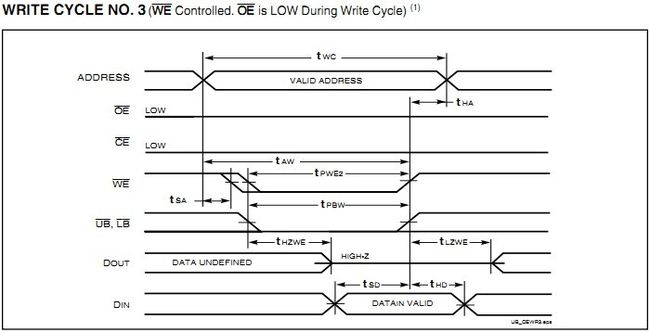
写操作时, 只需送地址ADDR的同时把nWE拉低( Tsa >= 0 ), 然后延时 THZWE 等待SRAM释放DATA总线后,
送出数据 DIN, 然后延时( Taw-Tsa-Thzwe ) 时间在把SRAM_WE拉高, 这时就把数据写入相应的地址;
读数据时,只需把需要读出的地址放到SRAM的地址总线上,然后延迟Taa时间后就可以读出数据了.
SRAM : IS61LV25616BL-10
CLOCK : 72MHz ( t = 13.88 ns )
写入数据 ( 三个时钟 )
1. nWE = 0, ADDR = wrAddr ( 1st clock rising edge ) [ Tsa 可以为 0, Addr 和 nWE 同时有效 ]
2. OE=1, DIN = wrData ( 2nd clock rising edge ) [ Tclk > (TSA+THZWE ) ]
3. nWE = 1, OE=0, ADDR = rdAddr, ( 3rd clock rising edge ) [ Thd 可以为 0, 撤销 nWE 的同时 释放数据总线 ]
读取数据 ( 一个时钟 )
4. rdData = DOUT, ADDR = next_rdAddr ( 4th clock rising edge )
5. rdData = DOUT, ADDR = next_rdAddr ( 5th clock rising edge )
持续读取任意地址数据
另外一种方法写入数据 ( 两个时钟 )
1. nWE = 0, ADDR = wrAddr, DIN = wrData ( 1st clock rising edge ) [ Tsa 可以为 0, Addr 和 nWE 同时有效 ]
2. OE=1, 驱动数据总线 ( 1st clock falling edge ) [ t/2 = 6.9 ns > Thzwe ( 5ns ) ] SRAM 已经释放数据总线
3. nWE = 1 , ( 2rd clock rising edge ), 等待 t/2 = 6.9ns > THD ( >= 0 )
4. OE=0, ADDR = rdAddr, ( 2rd clock falling edge ) [ Thd 可以为 0, 撤销 nWE 的同时 释放数据总线 ]
STM32 读取写入时序
Signals synchronization
● All controller output signals change on the rising edge of the internal clock (HCLK)
● In synchronous read and write mode, the output data changes on the falling edge of the memory clock (FSMC_CLK).
Asynchronous Mode
With the M29W129FL, we will use the Mode2 protocol. We will therefore not use any extended mode and
the timings will be the same for read and write operations.
In this case, the NOR memory controller needs three timing parameters:
ADDSET, DATAST and ADDHOLD.
ADDSET - Duration of the address setup phase = 0..15
ADDHOLD - Duration of the address hold phase = 1..15
DATAST - Duration of the data setup phase = 1..256
NOR Flash/PSRAM controller asynchronous transactions
Signals are synchronized by the internal clock HCLK. This clock is not issued to the memory
The FSMC always samples the data before de-asserting the chip select signal NE.
This guarantees that the memory data-hold timing constraint is met (chip enable high to data transition, usually 0 ns min.)
When extended mode is set, it is possible to mix modes A, B, C and D in read and write
(it is for instance possible to read in mode A and write in mode B).
读取一次至少 ADDSET + DATAST = 1 个时钟
写入数据至少需要 至少 ADDSET + DATAST + 1 = 2 个时钟
The one HCLK cycle at the end of the write transaction helps guarantee the address and data hold time after the NWE rising edge.
Due to the presence of this one HCLK cycle, the DATAST value must be greater than zero (DATAST > 0).
The one HCLK cycle at the end of the write transaction helps guarantee the address and
data hold time after the NWE rising edge. Due to the presence of this one HCLK cycle, the
DATAST value must be greater than zero (DATAST > 0).


