【龙芯1c库】移植硬浮点FPU
龙芯1c库是把龙芯1c的常用外设的常用功能封装为一个库,类似于STM32库。完整源码请移步到https://gitee.com/caogos/OpenLoongsonLib1c
龙芯1C上有硬浮点协处理器,整个移植过程主要参考《see mips run 中文版.pdf》中第7章“浮点支持”。文档《see mips run 中文版.pdf》可以在“https://gitee.com/caogos/OpenLoongsonLib1c/tree/master/doc”里面下载。
硬浮点FPU的使用没什么说的,就是在程序中需要使用浮点数时正常使用就行,本文重点放在移植上。
按图索骥
看看《see mips run 中文版.pdf》中怎么说的
文档《see mips run 中文版.pdf》的第7章用了一节的内容来详细讲解CPU复位后,应该怎样初始化FPU。如下图


文中已经描述得很清楚了。
第一步:使能协处理器1——FPU
第二步:设置控制/状态寄存器FCSR中的舍入模式和自陷使能
如果是裸机编程,执行以上两步就足够了;如果是移植到实时系统(比如RT-Thread)下,还需要执行
第三步:在中断和上下文切换时保存和恢复浮点寄存器。
浮点异常(自陷)
通常禁止全部浮点自陷
再来仔细看下上面那段话

这段话明确讲了通常是怎样设置舍入模式和自陷使能的。通常会禁止全部自陷,还要设置SR(FS)位让很小的结果返回零,这样可以免去一个到仿真程序的自陷。
浮点异常产生的原因

文中说“当一个浮点操作不能产生正确的结果时,就会发生一个MIPS异常”。那在哪些情况下不能产生正确的结果呢?

上图为FPU的控制/状态寄存器中关于异常的几个位的解释。共五种可能产生异常的原因——无效操作、除以零、上溢、下溢和非精确。在FPU的控制/状态寄存器中的位置如下

如果使能了FPU异常,并且也发生了异常,那么会触发cpu的异常,具体为协处理器0的cause寄存器中的FPE位被置位。根据前面的介绍,一般情况是禁止全部浮点异常,所以可以不用考虑触发cpu的异常。

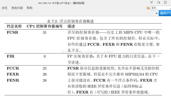
FPU寄存器简介
浮点控制状态寄存器
寄存器简介

控制/状态寄存器很重要,配置FPU就是配置这个寄存器。包括舍入模式和禁止全部中断都是操作这个寄存器。
另外还需要注意的一个地方是,操作控制/状态寄存器的汇编指令为ctc1和cfc1。其中cfc1用来读取寄存器的值,ctc1将值写入寄存器。
寄存器的读写
代码中将cfc1和ctc1封装为宏,并且进一步为控制/状态寄存器的读和写分别封装了一个宏,便于编程时直接调用。具体代码如下
/*
 * Macros to access the floating point coprocessor control registers
 */
#define read_32bit_cp1_register(source)                         \
({ int __res;                                                   \
	__asm__ __volatile__(                                   \
	".set\tpush\n\t"					\
	".set\treorder\n\t"					\
	/* gas fails to assemble cfc1 for some archs (octeon).*/ \
	".set\tmips1\n\t"					\
        "cfc1\t%0,"STR(source)"\n\t"                            \
	".set\tpop"						\
        : "=r" (__res));                                        \
        __res;})
#define write_32bit_cp1_register(register, value)   \
do {                                        \
    __asm__ __volatile__(                   \
        "ctc1\t%z0, "STR(register)"\n\t"      \
        : : "Jr" ((unsigned int)(value)));  \
} while (0)

#define read_c1_status()            read_32bit_cp1_register(CP1_STATUS)
#define read_c1_revision()          read_32bit_cp1_register(CP1_REVISION);
#define write_c1_status(val)        write_32bit_cp1_register(CP1_STATUS, val)
宏read_32bit_cp1_register(source)用于读取寄存器的值,宏write_32bit_cp1_register(register, value)向寄存器写入数据。
read_c1_status()读取控制/状态寄存器的值,read_c1_revision()读取浮点实现寄存器的值(浮点实现寄存器在后面介绍),write_c1_status(val)修改控制/状态寄存器。
其中,CP1_STATUS和CP1_REVISION为寄存器编号,如下
/*
 * Coprocessor 1 (FPU) register names
 */
#define CP1_REVISION   		$0
#define CP1_STATUS     		$31
寄存器的配置
根据上一章的分析,裸机编程时,FPU的初始化只需要两步。一:使能FPU,二:配置FPU的控制/状态寄存器(舍入模式、禁止全部中断)。用代码表示为
// 硬浮点初始化
void fpu_init(void)
{
    unsigned int c0_status = 0;
    unsigned int c1_status = 0;

    // 使能协处理器1--FPU
    c0_status = read_c0_status();
    c0_status |= (ST0_CU1 | ST0_FR);
    write_c0_status(c0_status);

    // 配置FPU
    c1_status = read_c1_status();
    c1_status |= (FPU_CSR_FS | FPU_CSR_FO | FPU_CSR_FN);    // set FS, FO, FN
    c1_status &= ~(FPU_CSR_ALL_E);                          // disable exception
    c1_status = (c1_status & (~FPU_CSR_RM)) | FPU_CSR_RN;   // set RN
    write_c1_status(c1_status);

    return ;
}
裸机编程中只需要在初始化的时候调用fpu_init(),就可以在裸机编程中使用硬浮点FPU了,
其中,FPU_CSR_FS、FPU_CSR_FO、FPU_CSR_FN、FPU_CSR_ALL_E、FPU_CSR_RM、FPU_CSR_RN为FPU的控制/状态寄存器的某个位域,用宏表示为
/*
 * FPU Status Register Values
 */
/*
 * Status Register Values
 */

#define FPU_CSR_FLUSH   0x01000000      /* flush denormalised results to 0 */
#define FPU_CSR_COND    0x00800000      /* $fcc0 */
#define FPU_CSR_COND0   0x00800000      /* $fcc0 */
#define FPU_CSR_COND1   0x02000000      /* $fcc1 */
#define FPU_CSR_COND2   0x04000000      /* $fcc2 */
#define FPU_CSR_COND3   0x08000000      /* $fcc3 */
#define FPU_CSR_COND4   0x10000000      /* $fcc4 */
#define FPU_CSR_COND5   0x20000000      /* $fcc5 */
#define FPU_CSR_COND6   0x40000000      /* $fcc6 */
#define FPU_CSR_COND7   0x80000000      /* $fcc7 */


/* FS/FO/FN */
#define FPU_CSR_FS      0x01000000
#define FPU_CSR_FO      0x00400000
#define FPU_CSR_FN      0x00200000

/*
 * Bits 18 - 20 of the FPU Status Register will be read as 0,
 * and should be written as zero.
 */
#define FPU_CSR_RSVD	0x001c0000

/*
 * X the exception cause indicator
 * E the exception enable
 * S the sticky/flag bit
*/
#define FPU_CSR_ALL_X   0x0003f000
#define FPU_CSR_UNI_X   0x00020000
#define FPU_CSR_INV_X   0x00010000
#define FPU_CSR_DIV_X   0x00008000
#define FPU_CSR_OVF_X   0x00004000
#define FPU_CSR_UDF_X   0x00002000
#define FPU_CSR_INE_X   0x00001000

#define FPU_CSR_ALL_E   0x00000f80
#define FPU_CSR_INV_E   0x00000800
#define FPU_CSR_DIV_E   0x00000400
#define FPU_CSR_OVF_E   0x00000200
#define FPU_CSR_UDF_E   0x00000100
#define FPU_CSR_INE_E   0x00000080

#define FPU_CSR_ALL_S   0x0000007c
#define FPU_CSR_INV_S   0x00000040
#define FPU_CSR_DIV_S   0x00000020
#define FPU_CSR_OVF_S   0x00000010
#define FPU_CSR_UDF_S   0x00000008
#define FPU_CSR_INE_S   0x00000004

/* Bits 0 and 1 of FPU Status Register specify the rounding mode */
#define FPU_CSR_RM	0x00000003
#define FPU_CSR_RN      0x0     /* nearest */
#define FPU_CSR_RZ      0x1     /* towards zero */
#define FPU_CSR_RU      0x2     /* towards +Infinity */
#define FPU_CSR_RD      0x3     /* towards -Infinity */
浮点实现寄存器
老规矩,先来看看《see mips run》怎么说的。


重点注意F64、L、W、D、S这几个位的值。
浮点实现寄存器的存取也是使用cfc1和ctc1,上一节已经给出了封装好的宏——read_c1_revision()
龙芯1c的芯片手册中说了龙芯1C有FPU,所以是否查看这个寄存器其实不太重要。但是如果要移植到实时系统(比如RT-Thread),就必须查看此寄存器的值了。特别是位域F64,这个位域告诉我们龙芯1C上的FPU是不是老式的MIPS I风格的浮点单元。
既然这样,那就在RT-Thread下把这个寄存器的值读取出来看看,如下

源码为
    rt_uint32_t c1_revision = 0;
    c1_revision = read_c1_revision();
    rt_kprintf("[%s] c1 FIR=0x%x\n", __FUNCTION__, c1_revision);
从上图可知,F64=0,即龙芯1C上的FPU为老式的MIPS I风格。不要看见这是,认为龙芯1C使用的是老式的MIPS I风格的FPU,感觉不爽,实际上很多嵌入式上的FPU都是使用的MIPS I风格的老式FPU,这对嵌入式应用来说足够了。
浮点运算需要用到的寄存器
寄存器简介

注意,这里的浮点寄存器是用于浮点运算的寄存器,不是前面提到的控制/状态寄存器和实现寄存器。这里的寄存器类似于CPU上的32个通用寄存器(t0,t1,v1,v2,a0,a1,sp,gp,k0,k1等)。

综上所述:龙芯1C使用的是老式的MIPS I风格的FPU,即ABI为o32。只有16个偶数号的寄存器可以用于计算,在实时系统RT-Thread的中断和上下文切换时需要保存的也就是这16个寄存器。
寄存器的读写
前面提到——FPU的控制/状态寄存器和实现寄存器使用cfc1和ctc1来存取寄存器,其中FPU控制/状态寄存器FCSR的编号为31,用$31表示;FPU实现寄存器FIR的编号为0,用$0表示。
本小节讨论的用于浮点运算的寄存器也有32个,只是龙芯1C的FPU为老式的MIPS I风格的,只使用编号为偶数的16个寄存器。分别用$f0, $f2, $f4, ...... , $f28, $f30。
注意,用于计算的32个寄存器编号中多了一个f。
与整数的运算类似,浮点运算也有加减乘除,为此还专门为FPU创建了一套指令,如下
移植FPU时,只需要在中断和上下文切换时保存用于浮点计算的16个寄存器就行,所以这里只关注Load/Store指令。


总结一下龙芯1C上FPU的Load/Store指令的要点:
1,只有16个偶数编号的寄存器参与浮点运算
2,优先使用合成指令,比如l.d $f0, 0(sp)
3,统一八字节对齐
尤其,特别注意字节对齐的问题。在中断和上下文切换时,先要将sp指针8字节对齐,然后再压栈或出栈。合成指令l.d $f0, 0(sp)实际上是将$f0和$f1两个寄存器中的值压栈了。
建议所有的栈都八字节对齐,包括实时系统中每个任务的栈。
中断处理程序中是不推荐有浮点运算的,其它比较耗时的也不允许,比如printf()打印函数等。正因为这个原因,所以裸机编程时没必要在中断中保存FPU寄存器,特殊情况除外。
源码清单
这里只展示裸机编程时涉及FPU的源码,更多的源码请移步到文章开头给出的git 地址里面查看,关于把FPU移植到RT-Thread会另外单独写一篇文章。
main.c
#include "../lib/ls1c_public.h"
#include "../lib/ls1c_gpio.h"
#include "../lib/ls1c_delay.h"
#include "../lib/ls1c_mipsregs.h"
#include "../example/test_gpio.h"
#include "../example/test_pwm.h"
#include "../example/test_delay.h"
#include "../example/test_simulate_i2c.h"
#include "../example/test_timer.h"
#include "../example/test_fpu.h"


// pmon提供的打印接口
struct callvectors *callvec;


// 硬浮点初始化
void fpu_init(void)
{
    unsigned int c0_status = 0;
    unsigned int c1_status = 0;

    // 使能协处理器1--FPU
    c0_status = read_c0_status();
    c0_status |= (ST0_CU1 | ST0_FR);
    write_c0_status(c0_status);

    // 配置FPU
    c1_status = read_c1_status();
    c1_status |= (FPU_CSR_FS | FPU_CSR_FO | FPU_CSR_FN);    // set FS, FO, FN
    c1_status &= ~(FPU_CSR_ALL_E);                          // disable exception
    c1_status = (c1_status & (~FPU_CSR_RM)) | FPU_CSR_RN;   // set RN
    write_c1_status(c1_status);

    return ;
}


void bsp_init(void)
{
    // 硬浮点初始化
    fpu_init();

    return ;
}


int main(int argc, char **argv, char **env, struct callvectors *cv)
{
	callvec = cv;       // 这条语句之后才能使用pmon提供的打印功能

    bsp_init();

    // -------------------------测试gpio----------------------
    /*
     * 测试库中gpio作为输出时的相关接口
     * led闪烁10次
     */
//    test_gpio_output();

    /*
     * 测试库中gpio作为输入时的相关接口
     * 按键按下时,指示灯点亮,否则,熄灭
     */
//    test_gpio_input();


    // ------------------------测试PWM--------------------------------
    // 测试硬件pwm产生连续的pwm波形
//    test_pwm_normal();

    // 测试硬件pwm产生pwm脉冲
//    test_pwm_pulse();

    /*
     * 测试gpio04复用为pwm,gpio06作为普通gpio使用
     * PWM0的默认引脚位GPIO06,但也可以复用为GPIO04
     * 当gpio06还是保持默认为pwm时,复用gpio04为pwm0,那么会同时在两个引脚输出相同的pwm波形
     * 本函数旨在证明可以在gpio04复用为pwm0时,还可以将(默认作为pwm0的)gpio06作为普通gpio使用
     */
//    test_pwm_gpio04_gpio06();

    // 测试pwm最大周期
//    test_pwm_max_period();


    // ------------------------测试软件延时--------------------------------
    // 测试延时函数delay_1ms()
//    test_delay_1ms();

    // 测试延时函数delay_1us()
//    test_delay_1us();

    // 测试延时函数delay_1s()
//    test_delay_1s();


    // ------------------------测试模拟I2C------------------------------
    // 测试模拟I2C
//    test_simulate_i2c_am2320();


    // ------------------------测试硬件定时器---------------------------
    // 测试硬件定时器的定时功能(读取中断状态位的方式判断是否超时)
//    test_timer_poll_time_out();

    // 测试硬件定时器的计时
//    test_timer_get_time();


    // ------------------------测试硬浮点(FPU)---------------------------
    // 测试使用硬浮点进行浮点数的加减乘除
    test_fpu();

	return(0);
}
ls1c_mipsregs.h
/*
 * This file is subject to the terms and conditions of the GNU General Public
 * License.  See the file "COPYING" in the main directory of this archive
 * for more details.
 *
 * Copyright (C) 1994, 1995, 1996, 1997, 2000, 2001 by Ralf Baechle
 * Copyright (C) 2000 Silicon Graphics, Inc.
 * Modified for further R[236]000 support by Paul M. Antoine, 1996.
 * Kevin D. Kissell, [email protected] and Carsten Langgaard, [email protected]
 * Copyright (C) 2000, 07 MIPS Technologies, Inc.
 * Copyright (C) 2003, 2004  Maciej W. Rozycki
 *
 * Change Logs:
 * Date           Author       Notes
 *
 */
#ifndef __MIPSREGS_H__
#define __MIPSREGS_H__

/*
 * The following macros are especially useful for __asm__
 * inline assembler.
 */
#ifndef __STR
#define __STR(x) #x
#endif
#ifndef STR
#define STR(x) __STR(x)
#endif

/*
 *  Configure language
 */
#ifdef __ASSEMBLY__
#define _ULCAST_
#else
#define _ULCAST_ (unsigned long)
#endif

/*
 * Coprocessor 0 register names
 */
#define CP0_INDEX 			$0
#define CP0_RANDOM		 	$1
#define CP0_ENTRYLO0 		$2
#define CP0_ENTRYLO1 		$3
#define CP0_CONF 			$3
#define CP0_CONTEXT 		$4
#define CP0_PAGEMASK 		$5
#define CP0_WIRED 			$6
#define CP0_INFO 			$7
#define CP0_BADVADDR 		$8
#define CP0_COUNT 			$9
#define CP0_ENTRYHI 		$10
#define CP0_COMPARE 		$11
#define CP0_STATUS 			$12
#define CP0_CAUSE 			$13
#define CP0_EPC 			$14
#define CP0_PRID 			$15
#define CP0_CONFIG 			$16
#define CP0_LLADDR 			$17
#define CP0_WATCHLO 		$18
#define CP0_WATCHHI 		$19
#define CP0_XCONTEXT 		$20
#define CP0_FRAMEMASK 		$21
#define CP0_DIAGNOSTIC 		$22
#define CP0_DEBUG 			$23
#define CP0_DEPC 			$24
#define CP0_PERFORMANCE 	$25
#define CP0_ECC 			$26
#define CP0_CACHEERR 		$27
#define CP0_TAGLO 			$28
#define CP0_TAGHI 			$29
#define CP0_ERROREPC 		$30
#define CP0_DESAVE 			$31

/*
 * R4640/R4650 cp0 register names.  These registers are listed
 * here only for completeness; without MMU these CPUs are not useable
 * by Linux.  A future ELKS port might take make Linux run on them
 * though ...
 */
#define CP0_IBASE 			$0
#define CP0_IBOUND 			$1
#define CP0_DBASE 			$2
#define CP0_DBOUND 			$3
#define CP0_CALG 			$17
#define CP0_IWATCH 			$18
#define CP0_DWATCH 			$19

/*
 * Coprocessor 0 Set 1 register names
 */
#define CP0_S1_DERRADDR0  	$26
#define CP0_S1_DERRADDR1  	$27
#define CP0_S1_INTCONTROL 	$20

/*
 * Coprocessor 0 Set 2 register names
 */
#define CP0_S2_SRSCTL	  	$12	/* MIPSR2 */

/*
 * Coprocessor 0 Set 3 register names
 */
#define CP0_S3_SRSMAP	  	$12	/* MIPSR2 */

/*
 *  TX39 Series
 */
#define CP0_TX39_CACHE		$7

/*
 * Coprocessor 1 (FPU) register names
 */
#define CP1_REVISION   		$0
#define CP1_STATUS     		$31

/*
 * FPU Status Register Values
 */
/*
 * Status Register Values
 */

#define FPU_CSR_FLUSH   0x01000000      /* flush denormalised results to 0 */
#define FPU_CSR_COND    0x00800000      /* $fcc0 */
#define FPU_CSR_COND0   0x00800000      /* $fcc0 */
#define FPU_CSR_COND1   0x02000000      /* $fcc1 */
#define FPU_CSR_COND2   0x04000000      /* $fcc2 */
#define FPU_CSR_COND3   0x08000000      /* $fcc3 */
#define FPU_CSR_COND4   0x10000000      /* $fcc4 */
#define FPU_CSR_COND5   0x20000000      /* $fcc5 */
#define FPU_CSR_COND6   0x40000000      /* $fcc6 */
#define FPU_CSR_COND7   0x80000000      /* $fcc7 */


/* FS/FO/FN */
#define FPU_CSR_FS      0x01000000
#define FPU_CSR_FO      0x00400000
#define FPU_CSR_FN      0x00200000

/*
 * Bits 18 - 20 of the FPU Status Register will be read as 0,
 * and should be written as zero.
 */
#define FPU_CSR_RSVD	0x001c0000

/*
 * X the exception cause indicator
 * E the exception enable
 * S the sticky/flag bit
*/
#define FPU_CSR_ALL_X   0x0003f000
#define FPU_CSR_UNI_X   0x00020000
#define FPU_CSR_INV_X   0x00010000
#define FPU_CSR_DIV_X   0x00008000
#define FPU_CSR_OVF_X   0x00004000
#define FPU_CSR_UDF_X   0x00002000
#define FPU_CSR_INE_X   0x00001000

#define FPU_CSR_ALL_E   0x00000f80
#define FPU_CSR_INV_E   0x00000800
#define FPU_CSR_DIV_E   0x00000400
#define FPU_CSR_OVF_E   0x00000200
#define FPU_CSR_UDF_E   0x00000100
#define FPU_CSR_INE_E   0x00000080

#define FPU_CSR_ALL_S   0x0000007c
#define FPU_CSR_INV_S   0x00000040
#define FPU_CSR_DIV_S   0x00000020
#define FPU_CSR_OVF_S   0x00000010
#define FPU_CSR_UDF_S   0x00000008
#define FPU_CSR_INE_S   0x00000004

/* Bits 0 and 1 of FPU Status Register specify the rounding mode */
#define FPU_CSR_RM	0x00000003
#define FPU_CSR_RN      0x0     /* nearest */
#define FPU_CSR_RZ      0x1     /* towards zero */
#define FPU_CSR_RU      0x2     /* towards +Infinity */
#define FPU_CSR_RD      0x3     /* towards -Infinity */


/*
 * R4x00 interrupt enable / cause bits
 */
#define IE_SW0          (_ULCAST_(1) <<  8)
#define IE_SW1          (_ULCAST_(1) <<  9)
#define IE_IRQ0         (_ULCAST_(1) << 10)
#define IE_IRQ1         (_ULCAST_(1) << 11)
#define IE_IRQ2         (_ULCAST_(1) << 12)
#define IE_IRQ3         (_ULCAST_(1) << 13)
#define IE_IRQ4         (_ULCAST_(1) << 14)
#define IE_IRQ5         (_ULCAST_(1) << 15)

/*
 * R4x00 interrupt cause bits
 */
#define C_SW0           (_ULCAST_(1) <<  8)
#define C_SW1           (_ULCAST_(1) <<  9)
#define C_IRQ0          (_ULCAST_(1) << 10)
#define C_IRQ1          (_ULCAST_(1) << 11)
#define C_IRQ2          (_ULCAST_(1) << 12)
#define C_IRQ3          (_ULCAST_(1) << 13)
#define C_IRQ4          (_ULCAST_(1) << 14)
#define C_IRQ5          (_ULCAST_(1) << 15)

/*
 * Bitfields in the R4xx0 cp0 status register
 */
#define ST0_IE					0x00000001
#define ST0_EXL					0x00000002
#define ST0_ERL					0x00000004
#define ST0_KSU					0x00000018
#  define KSU_USER					0x00000010
#  define KSU_SUPERVISOR			0x00000008
#  define KSU_KERNEL				0x00000000
#define ST0_UX					0x00000020
#define ST0_SX					0x00000040
#define ST0_KX 					0x00000080
#define ST0_DE					0x00010000
#define ST0_CE					0x00020000

/*
 * Setting c0_status.co enables Hit_Writeback and Hit_Writeback_Invalidate
 * cacheops in userspace.  This bit exists only on RM7000 and RM9000
 * processors.
 */
#define ST0_CO					0x08000000

/*
 * Bitfields in the R[23]000 cp0 status register.
 */
#define ST0_IEC                 0x00000001
#define ST0_KUC					0x00000002
#define ST0_IEP					0x00000004
#define ST0_KUP					0x00000008
#define ST0_IEO					0x00000010
#define ST0_KUO					0x00000020
/* bits 6 & 7 are reserved on R[23]000 */
#define ST0_ISC					0x00010000
#define ST0_SWC					0x00020000
#define ST0_CM					0x00080000

/*
 * Bits specific to the R4640/R4650
 */
#define ST0_UM					(_ULCAST_(1) <<  4)
#define ST0_IL					(_ULCAST_(1) << 23)
#define ST0_DL					(_ULCAST_(1) << 24)

/*
 * Enable the MIPS DSP ASE
 */
#define ST0_MX					0x01000000

/*
 * Bitfields in the TX39 family CP0 Configuration Register 3
 */
#define TX39_CONF_ICS_SHIFT		19
#define TX39_CONF_ICS_MASK		0x00380000
#define TX39_CONF_ICS_1KB 		0x00000000
#define TX39_CONF_ICS_2KB 		0x00080000
#define TX39_CONF_ICS_4KB 		0x00100000
#define TX39_CONF_ICS_8KB 		0x00180000
#define TX39_CONF_ICS_16KB 		0x00200000

#define TX39_CONF_DCS_SHIFT		16
#define TX39_CONF_DCS_MASK		0x00070000
#define TX39_CONF_DCS_1KB 		0x00000000
#define TX39_CONF_DCS_2KB 		0x00010000
#define TX39_CONF_DCS_4KB 		0x00020000
#define TX39_CONF_DCS_8KB 		0x00030000
#define TX39_CONF_DCS_16KB 		0x00040000

#define TX39_CONF_CWFON 		0x00004000
#define TX39_CONF_WBON  		0x00002000
#define TX39_CONF_RF_SHIFT		10
#define TX39_CONF_RF_MASK		0x00000c00
#define TX39_CONF_DOZE			0x00000200
#define TX39_CONF_HALT			0x00000100
#define TX39_CONF_LOCK			0x00000080
#define TX39_CONF_ICE			0x00000020
#define TX39_CONF_DCE			0x00000010
#define TX39_CONF_IRSIZE_SHIFT	2
#define TX39_CONF_IRSIZE_MASK	0x0000000c
#define TX39_CONF_DRSIZE_SHIFT	0
#define TX39_CONF_DRSIZE_MASK	0x00000003

/*
 * Status register bits available in all MIPS CPUs.
 */
#define  ST0_IM			    0x0000ff00
#define  STATUSB_IP0		8
#define  STATUSF_IP0		(_ULCAST_(1) <<  8)
#define  STATUSB_IP1		9
#define  STATUSF_IP1		(_ULCAST_(1) <<  9)
#define  STATUSB_IP2		10
#define  STATUSF_IP2		(_ULCAST_(1) << 10)
#define  STATUSB_IP3		11
#define  STATUSF_IP3		(_ULCAST_(1) << 11)
#define  STATUSB_IP4		12
#define  STATUSF_IP4		(_ULCAST_(1) << 12)
#define  STATUSB_IP5		13
#define  STATUSF_IP5		(_ULCAST_(1) << 13)
#define  STATUSB_IP6		14
#define  STATUSF_IP6		(_ULCAST_(1) << 14)
#define  STATUSB_IP7		15
#define  STATUSF_IP7		(_ULCAST_(1) << 15)
#define  STATUSB_IP8		0
#define  STATUSF_IP8		(_ULCAST_(1) <<  0)
#define  STATUSB_IP9		1
#define  STATUSF_IP9		(_ULCAST_(1) <<  1)
#define  STATUSB_IP10		2
#define  STATUSF_IP10		(_ULCAST_(1) <<  2)
#define  STATUSB_IP11		3
#define  STATUSF_IP11		(_ULCAST_(1) <<  3)
#define  STATUSB_IP12		4
#define  STATUSF_IP12		(_ULCAST_(1) <<  4)
#define  STATUSB_IP13		5
#define  STATUSF_IP13		(_ULCAST_(1) <<  5)
#define  STATUSB_IP14		6
#define  STATUSF_IP14		(_ULCAST_(1) <<  6)
#define  STATUSB_IP15		7
#define  STATUSF_IP15		(_ULCAST_(1) <<  7)
#define  ST0_CH				0x00040000
#define  ST0_SR				0x00100000
#define  ST0_TS				0x00200000
#define  ST0_BEV			0x00400000
#define  ST0_RE				0x02000000
#define  ST0_FR				0x04000000
#define  ST0_CU				0xf0000000
#define  ST0_CU0			0x10000000
#define  ST0_CU1			0x20000000
#define  ST0_CU2			0x40000000
#define  ST0_CU3			0x80000000
#define  ST0_XX				0x80000000	/* MIPS IV naming */

/*
 * Bitfields and bit numbers in the coprocessor 0 cause register.
 *
 * Refer to your MIPS R4xx0 manual, chapter 5 for explanation.
 */
#define  CAUSEB_EXCCODE		2
#define  CAUSEF_EXCCODE		(_ULCAST_(31)  <<  2)
#define  CAUSEB_IP			8
#define  CAUSEF_IP			(_ULCAST_(255) <<  8)
#define  CAUSEB_IP0			8
#define  CAUSEF_IP0			(_ULCAST_(1)   <<  8)
#define  CAUSEB_IP1			9
#define  CAUSEF_IP1			(_ULCAST_(1)   <<  9)
#define  CAUSEB_IP2			10
#define  CAUSEF_IP2			(_ULCAST_(1)   << 10)
#define  CAUSEB_IP3			11
#define  CAUSEF_IP3			(_ULCAST_(1)   << 11)
#define  CAUSEB_IP4			12
#define  CAUSEF_IP4			(_ULCAST_(1)   << 12)
#define  CAUSEB_IP5			13
#define  CAUSEF_IP5			(_ULCAST_(1)   << 13)
#define  CAUSEB_IP6			14
#define  CAUSEF_IP6			(_ULCAST_(1)   << 14)
#define  CAUSEB_IP7			15
#define  CAUSEF_IP7			(_ULCAST_(1)   << 15)
#define  CAUSEB_IV			23
#define  CAUSEF_IV			(_ULCAST_(1)   << 23)
#define  CAUSEB_CE			28
#define  CAUSEF_CE			(_ULCAST_(3)   << 28)
#define  CAUSEB_BD			31
#define  CAUSEF_BD			(_ULCAST_(1)   << 31)

/*
 * Bits in the coprocessor 0 config register.
 */
/* Generic bits.  */
#define CONF_CM_CACHABLE_NO_WA			0
#define CONF_CM_CACHABLE_WA				1
#define CONF_CM_UNCACHED				2
#define CONF_CM_CACHABLE_NONCOHERENT	3
#define CONF_CM_CACHABLE_CE				4
#define CONF_CM_CACHABLE_COW			5
#define CONF_CM_CACHABLE_CUW			6
#define CONF_CM_CACHABLE_ACCELERATED	7
#define CONF_CM_CMASK					7
#define CONF_BE							(_ULCAST_(1) << 15)

/* Bits common to various processors.  */
#define CONF_CU				(_ULCAST_(1) <<  3)
#define CONF_DB				(_ULCAST_(1) <<  4)
#define CONF_IB				(_ULCAST_(1) <<  5)
#define CONF_DC				(_ULCAST_(7) <<  6)
#define CONF_IC				(_ULCAST_(7) <<  9)
#define CONF_EB				(_ULCAST_(1) << 13)
#define CONF_EM				(_ULCAST_(1) << 14)
#define CONF_SM				(_ULCAST_(1) << 16)
#define CONF_SC				(_ULCAST_(1) << 17)
#define CONF_EW				(_ULCAST_(3) << 18)
#define CONF_EP				(_ULCAST_(15)<< 24)
#define CONF_EC				(_ULCAST_(7) << 28)
#define CONF_CM				(_ULCAST_(1) << 31)

/* Bits specific to the R4xx0.  */
#define R4K_CONF_SW			(_ULCAST_(1) << 20)
#define R4K_CONF_SS			(_ULCAST_(1) << 21)
#define R4K_CONF_SB			(_ULCAST_(3) << 22)

/* Bits specific to the R5000.  */
#define R5K_CONF_SE			(_ULCAST_(1) << 12)
#define R5K_CONF_SS			(_ULCAST_(3) << 20)

/* Bits specific to the RM7000.  */
#define RM7K_CONF_SE		(_ULCAST_(1) <<  3)
#define RM7K_CONF_TE		(_ULCAST_(1) << 12)
#define RM7K_CONF_CLK		(_ULCAST_(1) << 16)
#define RM7K_CONF_TC		(_ULCAST_(1) << 17)
#define RM7K_CONF_SI		(_ULCAST_(3) << 20)
#define RM7K_CONF_SC		(_ULCAST_(1) << 31)

/* Bits specific to the R10000.  */
#define R10K_CONF_DN		(_ULCAST_(3) <<  3)
#define R10K_CONF_CT		(_ULCAST_(1) <<  5)
#define R10K_CONF_PE		(_ULCAST_(1) <<  6)
#define R10K_CONF_PM		(_ULCAST_(3) <<  7)
#define R10K_CONF_EC		(_ULCAST_(15)<<  9)
#define R10K_CONF_SB		(_ULCAST_(1) << 13)
#define R10K_CONF_SK		(_ULCAST_(1) << 14)
#define R10K_CONF_SS		(_ULCAST_(7) << 16)
#define R10K_CONF_SC		(_ULCAST_(7) << 19)
#define R10K_CONF_DC		(_ULCAST_(7) << 26)
#define R10K_CONF_IC		(_ULCAST_(7) << 29)

/* Bits specific to the VR41xx.  */
#define VR41_CONF_CS		(_ULCAST_(1) << 12)
#define VR41_CONF_M16		(_ULCAST_(1) << 20)
#define VR41_CONF_AD		(_ULCAST_(1) << 23)

/* Bits specific to the R30xx.  */
#define R30XX_CONF_FDM		(_ULCAST_(1) << 19)
#define R30XX_CONF_REV		(_ULCAST_(1) << 22)
#define R30XX_CONF_AC		(_ULCAST_(1) << 23)
#define R30XX_CONF_RF		(_ULCAST_(1) << 24)
#define R30XX_CONF_HALT		(_ULCAST_(1) << 25)
#define R30XX_CONF_FPINT	(_ULCAST_(7) << 26)
#define R30XX_CONF_DBR		(_ULCAST_(1) << 29)
#define R30XX_CONF_SB		(_ULCAST_(1) << 30)
#define R30XX_CONF_LOCK		(_ULCAST_(1) << 31)

/* Bits specific to the TX49.  */
#define TX49_CONF_DC		(_ULCAST_(1) << 16)
#define TX49_CONF_IC		(_ULCAST_(1) << 17)  /* conflict with CONF_SC */
#define TX49_CONF_HALT		(_ULCAST_(1) << 18)
#define TX49_CONF_CWFON		(_ULCAST_(1) << 27)

/* Bits specific to the MIPS32/64 PRA.  */
#define MIPS_CONF_MT		(_ULCAST_(7) <<  7)
#define MIPS_CONF_AR		(_ULCAST_(7) << 10)
#define MIPS_CONF_AT		(_ULCAST_(3) << 13)
#define MIPS_CONF_M			(_ULCAST_(1) << 31)

/*
 * Bits in the MIPS32/64 PRA coprocessor 0 config registers 1 and above.
 */
#define MIPS_CONF1_FP		(_ULCAST_(1) <<  0)
#define MIPS_CONF1_EP		(_ULCAST_(1) <<  1)
#define MIPS_CONF1_CA		(_ULCAST_(1) <<  2)
#define MIPS_CONF1_WR		(_ULCAST_(1) <<  3)
#define MIPS_CONF1_PC		(_ULCAST_(1) <<  4)
#define MIPS_CONF1_MD		(_ULCAST_(1) <<  5)
#define MIPS_CONF1_C2		(_ULCAST_(1) <<  6)
#define MIPS_CONF1_DA		(_ULCAST_(7) <<  7)
#define MIPS_CONF1_DL		(_ULCAST_(7) << 10)
#define MIPS_CONF1_DS		(_ULCAST_(7) << 13)
#define MIPS_CONF1_IA		(_ULCAST_(7) << 16)
#define MIPS_CONF1_IL		(_ULCAST_(7) << 19)
#define MIPS_CONF1_IS		(_ULCAST_(7) << 22)
#define MIPS_CONF1_TLBS		(_ULCAST_(63)<< 25)

#define MIPS_CONF2_SA		(_ULCAST_(15)<<  0)
#define MIPS_CONF2_SL		(_ULCAST_(15)<<  4)
#define MIPS_CONF2_SS		(_ULCAST_(15)<<  8)
#define MIPS_CONF2_SU		(_ULCAST_(15)<< 12)
#define MIPS_CONF2_TA		(_ULCAST_(15)<< 16)
#define MIPS_CONF2_TL		(_ULCAST_(15)<< 20)
#define MIPS_CONF2_TS		(_ULCAST_(15)<< 24)
#define MIPS_CONF2_TU		(_ULCAST_(7) << 28)

#define MIPS_CONF3_TL		(_ULCAST_(1) <<  0)
#define MIPS_CONF3_SM		(_ULCAST_(1) <<  1)
#define MIPS_CONF3_MT		(_ULCAST_(1) <<  2)
#define MIPS_CONF3_SP		(_ULCAST_(1) <<  4)
#define MIPS_CONF3_VINT		(_ULCAST_(1) <<  5)
#define MIPS_CONF3_VEIC		(_ULCAST_(1) <<  6)
#define MIPS_CONF3_LPA		(_ULCAST_(1) <<  7)
#define MIPS_CONF3_DSP		(_ULCAST_(1) << 10)

/*
 * Bits in the MIPS32/64 coprocessor 1 (FPU) revision register.
 */
#define MIPS_FPIR_S			(_ULCAST_(1) << 16)
#define MIPS_FPIR_D			(_ULCAST_(1) << 17)
#define MIPS_FPIR_PS		(_ULCAST_(1) << 18)
#define MIPS_FPIR_3D		(_ULCAST_(1) << 19)
#define MIPS_FPIR_W			(_ULCAST_(1) << 20)
#define MIPS_FPIR_L			(_ULCAST_(1) << 21)
#define MIPS_FPIR_F64		(_ULCAST_(1) << 22)

/*
 * R10000 performance counter definitions.
 *
 * FIXME: The R10000 performance counter opens a nice way to implement CPU
 *        time accounting with a precission of one cycle.  I don't have
 *        R10000 silicon but just a manual, so ...
 */

/*
 * Events counted by counter #0
 */
#define CE0_CYCLES						0
#define CE0_INSN_ISSUED					1
#define CE0_LPSC_ISSUED					2
#define CE0_S_ISSUED					3
#define CE0_SC_ISSUED					4
#define CE0_SC_FAILED					5
#define CE0_BRANCH_DECODED				6
#define CE0_QW_WB_SECONDARY				7
#define CE0_CORRECTED_ECC_ERRORS		8
#define CE0_ICACHE_MISSES				9
#define CE0_SCACHE_I_MISSES				10
#define CE0_SCACHE_I_WAY_MISSPREDICTED	11
#define CE0_EXT_INTERVENTIONS_REQ		12
#define CE0_EXT_INVALIDATE_REQ			13
#define CE0_VIRTUAL_COHERENCY_COND		14
#define CE0_INSN_GRADUATED				15

/*
 * Events counted by counter #1
 */
#define CE1_CYCLES						0
#define CE1_INSN_GRADUATED				1
#define CE1_LPSC_GRADUATED				2
#define CE1_S_GRADUATED					3
#define CE1_SC_GRADUATED				4
#define CE1_FP_INSN_GRADUATED			5
#define CE1_QW_WB_PRIMARY				6
#define CE1_TLB_REFILL					7
#define CE1_BRANCH_MISSPREDICTED		8
#define CE1_DCACHE_MISS					9
#define CE1_SCACHE_D_MISSES				10
#define CE1_SCACHE_D_WAY_MISSPREDICTED	11
#define CE1_EXT_INTERVENTION_HITS		12
#define CE1_EXT_INVALIDATE_REQ			13
#define CE1_SP_HINT_TO_CEXCL_SC_BLOCKS	14
#define CE1_SP_HINT_TO_SHARED_SC_BLOCKS	15

/*
 * These flags define in which privilege mode the counters count events
 */
#define CEB_USER		8	/* Count events in user mode, EXL = ERL = 0 */
#define CEB_SUPERVISOR	4	/* Count events in supvervisor mode EXL = ERL = 0 */
#define CEB_KERNEL		2	/* Count events in kernel mode EXL = ERL = 0 */
#define CEB_EXL			1	/* Count events with EXL = 1, ERL = 0 */


#ifndef __ASSEMBLY__

/*
 * Macros to access the system control coprocessor
 */
#define __read_32bit_c0_register(source, sel)				\
({ int __res;								\
	if (sel == 0)							\
		__asm__ __volatile__(					\
			"mfc0\t%0, " #source "\n\t"			\
			: "=r" (__res));				\
	else								\
		__asm__ __volatile__(					\
			".set\tmips32\n\t"				\
			"mfc0\t%0, " #source ", " #sel "\n\t"		\
			".set\tmips0\n\t"				\
			: "=r" (__res));				\
	__res;								\
})

#define __write_32bit_c0_register(register, sel, value)			\
do {									\
	if (sel == 0)							\
		__asm__ __volatile__(					\
			"mtc0\t%z0, " #register "\n\t"			\
			: : "Jr" ((unsigned int)(value)));		\
	else								\
		__asm__ __volatile__(					\
			".set\tmips32\n\t"				\
			"mtc0\t%z0, " #register ", " #sel "\n\t"	\
			".set\tmips0"					\
			: : "Jr" ((unsigned int)(value)));		\
} while (0)

#define read_c0_index()			__read_32bit_c0_register($0, 0)
#define write_c0_index(val)		__write_32bit_c0_register($0, 0, val)

#define read_c0_random()		__read_32bit_c0_register($1, 0)
#define write_c0_random(val)	__write_32bit_c0_register($1, 0, val)

#define read_c0_entrylo0()		__read_32bit_c0_register($2, 0)
#define write_c0_entrylo0(val)	__write_32bit_c0_register($2, 0, val)

#define read_c0_entrylo1()		__read_32bit_c0_register($3, 0)
#define write_c0_entrylo1(val)	__write_32bit_c0_register($3, 0, val)

#define read_c0_conf()			__read_32bit_c0_register($3, 0)
#define write_c0_conf(val)		__write_32bit_c0_register($3, 0, val)

#define read_c0_context()		__read_32bit_c0_register($4, 0)
#define write_c0_context(val)	__write_32bit_c0_register($4, 0, val)

#define read_c0_userlocal()		__read_32bit_c0_register($4, 2)
#define write_c0_userlocal(val)	__write_32bit_c0_register($4, 2, val)

#define read_c0_pagemask()		__read_32bit_c0_register($5, 0)
#define write_c0_pagemask(val)	__write_32bit_c0_register($5, 0, val)

#define read_c0_wired()			__read_32bit_c0_register($6, 0)
#define write_c0_wired(val)		__write_32bit_c0_register($6, 0, val)

#define read_c0_info()			__read_32bit_c0_register($7, 0)

#define read_c0_cache()			__read_32bit_c0_register($7, 0)	/* TX39xx */
#define write_c0_cache(val)		__write_32bit_c0_register($7, 0, val)

#define read_c0_badvaddr()		__read_32bit_c0_register($8, 0)
#define write_c0_badvaddr(val)	__write_32bit_c0_register($8, 0, val)

#define read_c0_count()			__read_32bit_c0_register($9, 0)
#define write_c0_count(val)		__write_32bit_c0_register($9, 0, val)

#define read_c0_count2()		__read_32bit_c0_register($9, 6) /* pnx8550 */
#define write_c0_count2(val)	__write_32bit_c0_register($9, 6, val)

#define read_c0_count3()		__read_32bit_c0_register($9, 7) /* pnx8550 */
#define write_c0_count3(val)	__write_32bit_c0_register($9, 7, val)

#define read_c0_entryhi()		__read_32bit_c0_register($10, 0)
#define write_c0_entryhi(val)	__write_32bit_c0_register($10, 0, val)

#define read_c0_compare()		__read_32bit_c0_register($11, 0)
#define write_c0_compare(val)	__write_32bit_c0_register($11, 0, val)

#define read_c0_compare2()		__read_32bit_c0_register($11, 6) /* pnx8550 */
#define write_c0_compare2(val)	__write_32bit_c0_register($11, 6, val)

#define read_c0_compare3()		__read_32bit_c0_register($11, 7) /* pnx8550 */
#define write_c0_compare3(val)	__write_32bit_c0_register($11, 7, val)

#define read_c0_status()		__read_32bit_c0_register($12, 0)
#define write_c0_status(val)	__write_32bit_c0_register($12, 0, val)

#define read_c0_cause()			__read_32bit_c0_register($13, 0)
#define write_c0_cause(val)		__write_32bit_c0_register($13, 0, val)

#define read_c0_epc()			__read_32bit_c0_register($14, 0)
#define write_c0_epc(val)		__write_32bit_c0_register($14, 0, val)

#define read_c0_prid()			__read_32bit_c0_register($15, 0)

#define read_c0_ebase()			__read_32bit_c0_register($15, 1)
#define write_c0_ebase(val)		__write_32bit_c0_register($15, 1, val)

#define read_c0_config()		__read_32bit_c0_register($16, 0)
#define read_c0_config1()		__read_32bit_c0_register($16, 1)
#define read_c0_config2()		__read_32bit_c0_register($16, 2)
#define read_c0_config3()		__read_32bit_c0_register($16, 3)
#define write_c0_config(val)	__write_32bit_c0_register($16, 0, val)
#define write_c0_config1(val)	__write_32bit_c0_register($16, 1, val)
#define write_c0_config2(val)	__write_32bit_c0_register($16, 2, val)
#define write_c0_config3(val)	__write_32bit_c0_register($16, 3, val)


/*
 * Macros to access the floating point coprocessor control registers
 */
#define read_32bit_cp1_register(source)                         \
({ int __res;                                                   \
	__asm__ __volatile__(                                   \
	".set\tpush\n\t"					\
	".set\treorder\n\t"					\
	/* gas fails to assemble cfc1 for some archs (octeon).*/ \
	".set\tmips1\n\t"					\
        "cfc1\t%0,"STR(source)"\n\t"                            \
	".set\tpop"						\
        : "=r" (__res));                                        \
        __res;})
#define write_32bit_cp1_register(register, value)   \
do {                                        \
    __asm__ __volatile__(                   \
        "ctc1\t%z0, "STR(register)"\n\t"      \
        : : "Jr" ((unsigned int)(value)));  \
} while (0)

#define read_c1_status()            read_32bit_cp1_register(CP1_STATUS)
#define read_c1_revision()          read_32bit_cp1_register(CP1_REVISION);
#define write_c1_status(val)        write_32bit_cp1_register(CP1_STATUS, val)


#endif /* end of __ASSEMBLY__ */

#endif /* end of __MIPSREGS_H__ */
test_fpu.h
// 硬浮点测试用例的头文件

#ifndef __OPENLOONGSON_TEST_FPU_H
#define __OPENLOONGSON_TEST_FPU_H


// 测试使用硬浮点进行浮点数的加减乘除
void test_fpu(void);


#endif
test_fpu.c
// 硬浮点测试用例的源文件


#include "../lib/ls1c_public.h"


// 每个测试用例中for循环的最大值
#define TEST_FPU_MAX_COUNT          (1000)


// 使用硬浮点执行浮点数的加法
void test_fpu_add(void)
{
    unsigned int i = 0;
    float sum_f = 0.0;
    unsigned int *sum_p = (unsigned int *)&sum_f;

    myprintf("\n\n----------------------%s-------------------\n", __FUNCTION__);
    for (i=0; i
测试FPU是否移植成功的测试用例中,分别执行1000次浮点数的加、减、乘和除。测试时将浮点数所占的4个字节打印出来了。可以另外在linux下用龙芯1c执行一篇这个测试函数,然后对比查看打印结果是否一致,来判断浮点运算是否正确。
1c库gitee上最新的代码已经可以使用printf的%f来打印浮点数了。
另外,这里也只测试了单精度浮点。
感谢耐心看完!