DDR4 Bank Groups in Embedded Applications
https://www.synopsys.com/designware-ip/technical-bulletin/ddr4-bank-groups.html
By Graham Allan
DDR4 represents the most complex DRAM transition since asynchronous DRAMs made way for the original SDRAM back in the 1990s. SoC designers need to learn about the subtleties of DDR4 SDRAM to ensure that their designs fully benefit from this new standard’s lower system power and higher overall bandwidth.
While DDR4 is still somewhat evolutionary, it does contain over twenty new features as compared to DDR3, many of which have a significant impact on how memory is used in an embedded system application. This article focuses on the effective use of DDR4 bank groups for the highest data efficiency.
What are DDR4 SDRAM Bank Groups?
The bank groups feature used in DDR4 SDRAMs was borrowed from the GDDR5 graphics memories. In order to understand the need for bank groups, the concept of DDR SDRAM prefetch must be understood. Prefetch is the term describing how many words of data are fetched every time a column command is performed with DDR memories. Because the core of the DRAM is much slower than the interface, the difference is bridged by accessing information in parallel and then serializing it out the interface. For example, DDR3 prefetches eight words, which means that every time a read or a write operation is performed, it is performed on eight words of data, and bursts out of, or into, the SDRAM over four clock cycles on both clock edges for a total of eight consecutive operations. Fundamentally, it can be thought of that for DDR3’s prefetch of eight, the interface is eight times faster than the DRAM core.
The downside to the prefetch is that it effectively determines the minimum burst length for the SDRAMs. For example, it is very difficult to have an efficient burst length of four words with DDR3’s prefetch of eight. The bank group feature allows designers to keep a smaller prefetch while increasing performance as if the prefetch is larger.
Since the core speed of the DRAM does not change significantly from generation to generation, the prefetch has increased with every DDR generation to offer increased speed at the SDRAM interface. However, continuing the trend with DDR4 would have required DDR4 to adopt a prefetch of sixteen. This change would make the DRAMs much larger because of all the wires that have to be included. It would make the DRAMs too expensive, so designers saved cost by not going to a prefetch of sixteen. More importantly, a sixteen word prefetch would not match the 64 byte cache line size common in today’s computers. With a 64 bit or 72 bit interface in a typical compute environment, which uses a 64 byte cache line, a prefetch of eight along with a burst length of eight is a better match. Any such misalignment of cache line size and burst length can have a negative impact on the performance of embedded systems.
DDR4 Prefetch & Performance
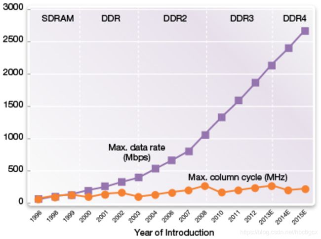
To understand how prefetch affects performance, it is helpful to look at what has happened with SDRAMs over time. Figure 1 shows the maximum data rate for each generation of SDRAM compared to the maximum column cycle. Figure 1 shows that the core is quite slow and has changed little over time whereas the interface speed has increased significantly over time. The core of the SDRAM has not become faster over time, largely because any benefits derived from a smaller process have been offset by the much larger SDRAM, due to its greater capacity. Designers end up fighting increasing capacity, which is complemented by the miniaturization of the process. However, the I/O is consistently faster with every generation. How is that possible? Well, that’s where the prefetch comes in.

Figure 1: SDRAM Performance Scaling
When the original SDR (single data rate) SDRAM was introduced, there was no need for a prefetch. Every time a column cycle was executed, it accessed one word of data, and that was pushed out of the SDRAM. Now, while SDRAM actually did have something called a 2N rule, which could accommodate a prefetch of two, 2N was viewed as a restrictive part of the specification and all of the SDRAM devices which eventually became commodity devices had a prefetch of one. However, once DDR SDRAM was introduced, the core could no longer keep up with the bandwidth required of the SDRAM. That was the beginning of the separation between the maximum data rate on the pins and the column cycle inside, as shown in Figure 2.
![]()
Figure 2: SDRAM Performance Scaling Enabled by Prefetch
This separation has grown over time. With DDR2’s prefetch of four and DDR3’s prefetch of eight, the separation grew even wider. DDR4 is still using a prefetch of eight, but has introduced the concept of bank groups to avoid the negative repercussions of a larger prefetch.
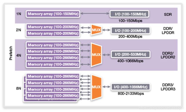
Figure 3 shows how the prefetch has evolved through four generations of SDRAM, from SDR SDRAM to DDR3 SDRAM. For any single column operation (e.g., read or write), the number of words accessed at once is represented by the number of memory arrays, along with the approximate cycle time (MHz) that it takes to get those words out of or into the core of the SDRAM.
The top row shows SDR SDRAM. Back in the mid -’90s, the memory array speed matched the I/O speed. Soon, a prefetch of two, or a 2N prefetch for DDR (which is also applicable to LPDDR) was introduced to enable higher data rates than the SDRAM core could match. The multiplexer shown can access these two words, and then they are muxed out on the interface, on one rising edge and one falling edge of the clock. This pattern continues through DDR3/LPDDR3 with its 8N prefetch.

Figure 3: Historical DRAM Prefetch
DDR4 and Bank Groups
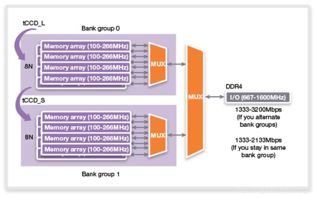
The question becomes: how does this apply to DDR4 and its 8N prefetch? If the trend shown in Figure 3 were followed with DDR4, DDR4 would have a prefetch of sixteen, but we have seen that is not desirable. DDR4 avoids this issue by introducing the concept of bank groups. With bank groups, a prefetch of eight is executed in one bank group, and another prefetch of eight can be executed in another independent bank group. The bank groups are separate entities, such that they allow a column cycle to complete within a bank group, but that column cycle does not impact what is happening in another bank group. Effectively, the DDR4 SDRAM can time division multiplex its internal bank groups in order to hide the fact that the internal SDRAM core cycle time takes longer than a burst of eight requires on the interface. Figure 4 shows how this process looks for a x16 DDR4 SDRAM with two bank groups, which are often used in embedded applications.

Figure 4: DDR4 Solution to Prefetch of Eight
New Bank Groups Specifications
The introduction of bank groups comes with new specifications for DDR4. Two key specifications are tCCD_S and tCCD_L. The “CCD” stands for “column to column delay”, or “command to command delay” on the column side. The “_S” stands for “short”, and the “_L” stands for “long”.
When a command is started in one bank group with an 8N prefetch, the prefetch must be allowed to finish, requiring the entire cycle time of the group to finish. Going from one bank group to another bank group does not have any dependencies on these specifications. That is the case for using the tCCD_S specification, which, at four clock cycles, is unrestrictive in a manner similar to DDR3.
However, here’s the big gotcha. Going from command to command while staying within the same bank group, requires attention to DDR4’s new tCCD_L specification, which is typically greater than four clock cycles. This case can impact your design’s performance, which is particularly important in embedded applications. Figure 5 highlights the difference between tCCD_S and tCCD_L.

Figure 5: tCCD_L and tCCD_S in DDR4 Bank Groups
New tCCD Specifications, Big Impact
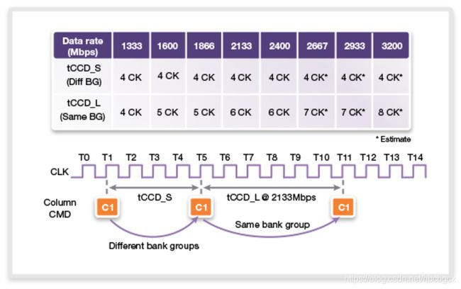
As shown in Figure 6, going between different bank groups with DDR4 requires a delay of four clock cycles. Four clock cycles matches a burst length of eight. Because four clock cycles is eight clock edges, both rising and falling, a burst length of eight puts out data, or receives data, on every clock edge in that four-clock period very efficiently. In this case, there is no wasted bus bandwidth. One command can follow another without any wasted cycles on the bus where data is not being transferred.

Figure 6: Bank Group Defines tCCD Parameters Differently Between the Same Bank Group and a Different Bank Group
However, when staying within the same bank group starting at 1,600 Mbps, the tCCD_L specification requires more than four clocks. It requires five clocks for 1,600 and 1,866 Mbps, and at 2,133 Mbps, it requires six clocks. The timing diagram underneath the table in Figure 6 shows that going between different bank groups can have four clock cycles between the access points. Staying within the same bank group at, e.g., 2,133 Mbps, requires six clock cycles between the column commands. However, only 4 clock cycles are required to transfer the data. Two clock cycles, or 33% of the bus bandwidth, just became unusable.
Scheduling Traffic for Efficient Bank Group Use
The timing diagram in Figure 7 shows the impact of DDR4’s bank groups in a 1600 Mbps example. The tCCD_L long specification of five means that five clock cycles are required between column commands within the same bank group. The highlighted area shows the end result: When there are five clock cycles used, there is one wasted clock cycle without any data going into or out of the device. This becomes a much bigger issue at higher data rates, where tCCD_L becomes six or seven, or even eight clock cycles. In the case of eight, trying to stay within the same bank group effectively gives away half of the bandwidth.

Figure 7: Potential Wasted Clock Cycles Between Column Commands1
DDR4 offers a host of new features for embedded systems that can enhance performance and bandwidth when implemented correctly. Synopsys provides a complete DDR4 solution, including the DDR4 multiPHY, Enhanced Universal DDR Memory Controller, and Verification IP. Synopsys’ DesignWare DDR4 solution supports DDR4 and DDR3, as well as low-power memories (LPDDR2 and LPDDR3), all in a single solution. For more information on how Synopsys IP can benefit your system, visit the Synopsys DDR webpage.
Sources:
1 JEDEC Standard: DDR4 SDRAM (JESD79-4). JEDEC Solid State Technology Association. September 2012.