HDLBits 代码输出 Circuits(二)
(1)combinational Logic
对于真值表,可以化简为“积之和”的形式
(静态冒险:电路的输出在某种输入作用下,不应当发生跳变时却发生了跳变的情况。由于不同扇出路径上的不同传播时延造成的,在输出毛刺是由单个输入信号发生变化而造成时,可以通过在输出表达式的覆盖中引入冗余与项就能够消除静态冒险)
1->0->1 静态1冒险;0->1->0 静态0冒险
(动态冒险:原本期望一个输入变化会造成输出的一次变化,实际上却导致了输出到达期望值之前发生了两次或多次变化)
One simple method to create a circuit that implements the truth table’s function is to express the function in sum-of-products form. Sum (meaning OR) of products (meaning AND) means using one N-input AND gate per row of the truth table (to detect when the input matches each row), followed by an OR gate that chooses only those rows that result in a ‘1’ output.
使用卡诺图(product-of-sums积之和,sum-of-products和之积) 的形式,覆盖静态冒险
When designing circuits, one often has to think of the problem “backwards”, starting from the outputs then working backwards towards the inputs.
注意按照工业代码的写法,还是需要会使用assign 语句写组合逻辑
例如:You are given a four-bit input vector in[3:0]. We want to know some relationships between each bit and its neighbour:
- out_both: Each bit of this output vector should indicate whether both the corresponding input bit and its neighbour to the left (higher index) are ‘1’. For example, out_both[2] should indicate if in[2] and in[3] are both 1. Since in[3] has no neighbour to the left, the answer is obvious so we don’t need to know out_both[3].
- out_any: Each bit of this output vector should indicate whether any of the corresponding input bit and its neighbour to the right are ‘1’. For example, out_any[2] should indicate if either in[2] or in[1] are 1. Since in[0] has no neighbour to the right, the answer is obvious so we don’t need to know out_any[0].
- out_different: Each bit of this output vector should indicate whether the corresponding input bit is different from its neighbour to the left. For example, out_different[2] should indicate if in[2] is different from in[3]. For this part, treat the vector as wrapping around, so in[3]'s neighbour to the left is in[0].
module top_module(
    input [3:0] in,
    output reg [2:0] out_both,
    output reg [3:1] out_any,
    output reg [3:0] out_different );
    always@(*)
        begin
            integer i,j,k;
            for(i=0;i<=2;i=i+1)
                begin
                    if(in[i]==1)
                        out_both[i]=in[i+1]&in[i];
                    else
                        out_both[i]=0;
                end
            for(j=1;j<=3;j=j+1)
                begin
                    if(in[j]==1||in[j-1]==1)
                        out_any[j]=1;
                    else
                        out_any[j]=0;
                end
            for(k=0;k<=2;k=k+1)
                begin
                    out_different[k]=in[k]^in[k+1];
                end
            out_different[3]=in[3]^in[0];
        end
endmodule
与下面的assign 写法的组合逻辑功能相同:
module top_module (
	input [3:0] in,
	output [2:0] out_both,
	output [3:1] out_any,
	output [3:0] out_different
);

	// Use bitwise operators and part-select to do the entire calculation in one line of code
	// in[3:1] is this vector:   					 in[3]  in[2]  in[1]
	// in[2:0] is this vector:   					 in[2]  in[1]  in[0]
	// Bitwise-OR produces a 3 bit vector.			   |      |      |
	// Assign this 3-bit result to out_any[3:1]:	o_a[3] o_a[2] o_a[1]

	// Thus, each output bit is the OR of the input bit and its neighbour to the right:
	// e.g., out_any[1] = in[1] | in[0];
	// Notice how this works even for long vectors.
	assign out_any = in[3:1] | in[2:0];

	assign out_both = in[2:0] & in[3:1];

	// XOR 'in' with a vector that is 'in' rotated to the right by 1 position: {in[0], in[3:1]}
	// The rotation is accomplished by using part selects[] and the concatenation operator{}.
	assign out_different = in ^ {in[0], in[3:1]};

endmodule
overflow detect:
A signed overflow occurs when adding two positive numbers produces a negative result, or adding two negative numbers produces a positive result. There are several methods to detect overflow: It could be computed by comparing the signs of the input and output numbers, or derived from the carry-out of bit n and n-1.
module top_module (
    input [7:0] a,
    input [7:0] b,
    output [7:0] s,
    output overflow
); //
 assign s=a+b;
    assign overflow=((a[7]==b[7])&(s[7]!=a[7]))?1:0;
endmodule
(2)sequential Logic
edgedetect1(detect an edge):

module top_module (
    input clk,
    input [7:0] in,
    output  [7:0] pedge
);
    reg [7:0] pedge1;
    reg [7:0] pedge2;
    always@(posedge clk)
    begin
            pedge1<=in;
        	pedge2<=pedge1;
    end
    assign pedge=pedge1&~pedge2;
endmodule
edgedetect2(detect both edges)

module top_module (
    input clk,
    input [7:0] in,
    output [7:0] anyedge
);
    reg [7:0] pedge1;
    reg [7:0] pedge2;
    always@(posedge clk)
        begin
            pedge1<=in;
            pedge2<=pedge1;
        end
    assign anyedge=pedge1&~pedge2|~pedge1&pedge2;//异或即可
endmodule
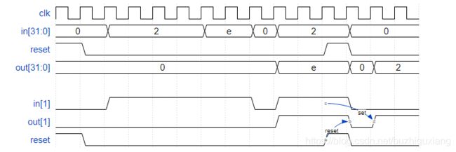
module top_module (
    input clk,
    input reset,
    input [31:0] in,
    output reg [31:0] out
);
    reg [31:0] in1;
    always@(posedge clk)
    begin
      if(reset)
          out<=0;
      else
          out<=out|(in1&~in);
    end
              always@(posedge clk)
                  begin
                      in1<=in;
                  end
endmodule
Dualedge
A dual-edge triggered flip-flop is triggered on both edges of the clock. However, FPGAs don’t have dual-edge triggered flip-flops, and always @(posedge clk or negedge clk) is not accepted as a legal sensitivity list.
Build a circuit that functionally behaves like a dual-edge triggered flip-flop:

count10
module top_module(
	input clk,
	input reset,
	output reg [3:0] q);

	always @(posedge clk)
		if (reset || q == 9)	// Count to 10 requires rolling over 9->0 instead of the more natural 15->0
			q <= 0;
		else
			q <= q+1;

endmodule
