光调制器通过对电压或电场的变化来控制输出光的吸收率、折射率、相位或振幅的变化。其根据各种不同形式的电光、声光、磁光效应、量子陷Stark效应和载流子的色散效应等,调控光发射机发射的光信号的振幅和状态,再进入光纤进行传播。目前,硅基电吸收调制器由于较弱的电光效应所以尺寸较大;目前,锗与其他化合物半导体调制器难以硅基集成;而它们的调制光谱范围通常比较窄。
石墨烯由于其零带隙可以吸收很宽频率范围的光,加之其超高的迁移率,所以在光调制器上可以充分发挥其优势。
2011年, Ming Liu 发表在Nature 474 64-67的Journal “A graphene-based broadband optical modulator”首次制备出光电效应石墨烯调制器,该调制器基于的原理为"...the broad optical absorption in graphene can be controlled through electrical gating: by shifting the electronic Fermi level, one can controllably change graphene's optical transition."。
The structure of the electrabsorption modulator is schematically illustrated in Fig.1:
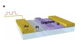
Figre 1.A graphene-based waveguide-integrated optical modulator
在硅波导上铺上一层单层石墨烯,中间用氧化铝隔开,波导是掺杂的并通过薄层的硅与电极相连,通过外加偏置电压控制费米能级的高低来控制光的吸收与透射。(原文:"A 50-nm-thick Si layer was used to connect the 250-nm-thick Si bus waveguide and one of the gold electrodes.Both the silicon layer and the waveguide were shallowly doped with boron to reduce the sheet resistance. A spacer of 7-nm-thick Al2O3 was then uniformly deposited on the surface of the waveguide by atom layer deposition. A graphene sheet grown by chemical vapour deposition was then machanically transferred onto the Si waveguide. To further reduce the access resistance of the device, the counter electrode was extended towards the bus waveguide by depositing a platium(10nm) film on the top of the graphene layer..."。)
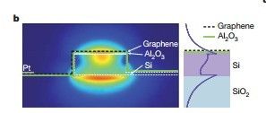
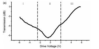
Figure 2 displays the transmission of 1.53μm photons through the waveguide at different drive voltages,VD:

Figure2 Static eletro-optical response of the device at different drive
在图中,只有费米能级位于阈值正负hv0/2之间时,才可能有光吸收,其它情况透射。(At low drive voltage (-1V
2012年,Ming Liu又在材料学顶级期刊Nano Letters发表Letters “Double-Layer Graphene Optical Modulator”,其采用双层石墨烯作为有源区的波导光调制器,采用一种类似p-氧化物-n的结构,直接利用石墨烯代替硅与金属电极形成接触。(By using two graphene layers and an oxide layer in between to forn a p-oxide-n like junction, this modulator operates at 1GHz with a high modulation depth (0.16dBμm-1) at a moderate drive voltage(5V).)。
制作工艺过程如下:The fabricate starts with commercial silicon-on-insulator(SOI) wafers with a device layer thickness of 340nm and a buried-oxide thickness of 2μm. A 400 nm wide silicon waveguide with both ends conected to a pair of grating couplers were fabricated using deep reactive-ion etch. Atomic layer deposition(ALD) technique was then employed to conformally coat a 5nm thick Al2O3 isolation layer to prevent potential carrier injectios from the bottom graphene layer into the silicon. Chip-sized graphene sheet, prepared on Cu film by CVD method, was first pretected by 200 nm thick poly film which was backed at 110C for 10 min.After the Cu film was removed by FeCl3 solution, the graphene sheet was then rinsed and transferred on the waveguides for overnight baking.
调制器结构如下图所示:
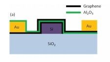
这样既可以增加光的吸收又减少的插入损耗,得到了0.16dBμm-1的调制深度,1GHz响应带宽的光调制器。
以上集成波导结构的调制器达到了很高的调制速率,同时小尺寸的波导结构也限制了其应用范围。尤其需要很低插入损耗的自由空间中,例如高Q值激光谐振腔中的振幅调制。针对此问题,Lee在2010年在光学顶级期刊OE上发表Journal "Broadband graphene electro-optic modulators with sub-wavelengtj thickness",改调制器在蓝宝石衬底上制作,以单层CVD生长石墨烯为有源区(直径为100μm的原型),通过两个电极之间的加电压来改变石墨烯中费米能级的位置和合理设计石墨烯与银之间的Ta2O5绝缘介质的厚度达到光调制的目的,其可以实现1Hz-100MHz的频率调制。这一大尺寸(有源区>7850μm2)的器件为其在激光器和有源干涉仪等光电器件上的应用提供了可能性,背面电极的银同时起到了高反射率反射镜的作用,石墨烯与银之间的Ta2O5绝缘介质的厚度直接影响了石墨烯费米能级的位置,进而影响光吸收的情况,其可以作为一个设计的自由度来根据实际需要设计其具体尺寸。
目前石墨烯光调制器的原型器件虽然取得重要进展,但其调制速率仍然受到限制,这主要是由于器件串联电阻导致的RC时间常数的限制,高的串联电阻主要是由于石墨烯与电极接触所形成的,因此,寻找减小石墨烯金属接触电阻的有效途径有望进一步提高石墨烯光调制器的速率。