思科2018校园招聘硬件笔试试题 及其答案
看到有同学感兴趣再分享一篇
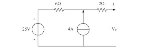
1、Which is the Thevenin equivalent for the circuit below?
A VO=49+8I
B VO=49-8I
C VO=25-8I
D VO=25-6I
正确答案:B
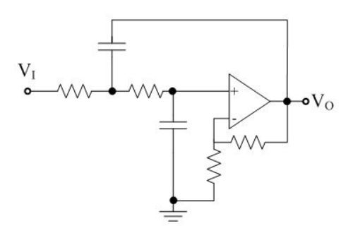
2、The circuit below is used for:
A low pass filter
B high pass filter
C band pass filter
D band stop filter
正确答案:A
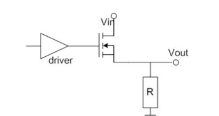
3、For the following circuitry, assuming the driver is outputting 2.5V, Vin is 5V, Vgs(th) is 1.5V and R is 1M ohm, where is the FET’s quiescent point (Q-point) location?
ACut-off region
BTriode region
CSaturation region
DPre-pinch off region
正确答案:C
(4/40) Given the following design, which one is the correct waveform for output Y?
正确答案:C
5、Which of the following terminology is not for the PCIE?
AInterrupt signal
BReceiver detection
CGen-2 5Gbps speed
DMax x16 lanes
EACK/NACK message
正确答案:A
6、 The passive probe is the most widely used general-purpose probe. The diagram below is the compensated attenuator in a probe with attenuation X10, what is the value of the C ideally?
A1pF
B9pF
C18pF
D2pF
正确答案:D
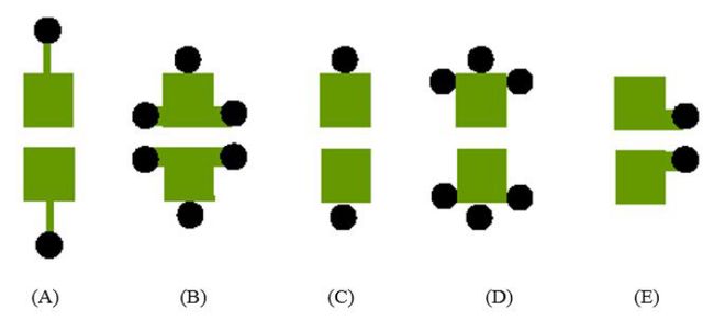
7、Which of the following circuitry is perfectly diff-signal termination designed?
正确答案:A
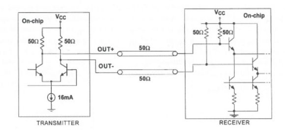
8、The following diagram shows the input and output structure of which type of interface?
A LVPECL
B LVDS
C CML
D CMOS
正确答案:C
9、For the following I2C timing diagram, which statement is correct?
ASTART condition is not correct
BThis is a I2C read operation
CSlave address is “0101101”
DSTOP condition is not correct
正确答案:D
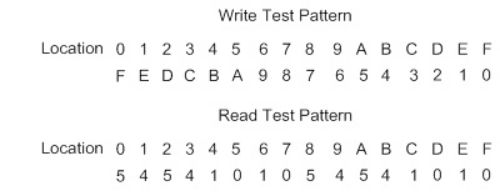
10、In the memory test program, we wrote an inverted pattern into SRAM on 16 locations starting from location 0. After read it back, we found the pattern does not match what we wrote. Which of the following statement is true?
A The address bit 0 is stuck at fault; The data bit 2 is stuck at fault
B The address bit 1 is stuck at fault; The data bit 3 is stuck at fault
C The address bit 2 is stuck at fault; The data bit 0 is stuck at fault
D The address bit 3 is stuck at fault; The data bit 1 is stuck at fault
正确答案:B
11、In the following circuit, the frequency at the output
Ahalf the input frequency
Bsame as input frequency
Ctwice the input frequency
Dfour times the input frequency
正确答案:C
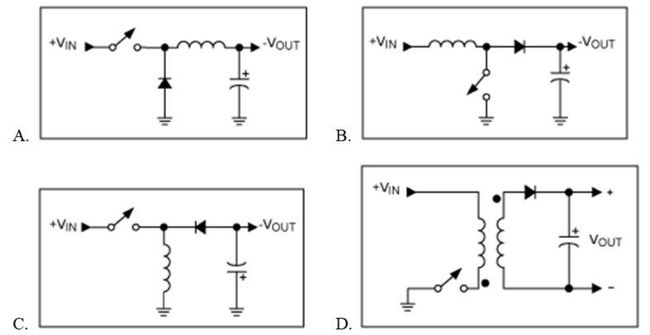
12、There are four popular DC-DC converters topology below, which one is the boost (step up) topology converter?
正确答案:B
13、Which ones of the following are NOT common methods to reduce EMI when routing high speed signal:
AKeep consecutive reference plane for the signal trace, don't cross difference power plane.
BIncrease trace width
CWhen signal trace changes layer, place some vias or bypass capacitors that connect to power or ground plane
DReduce the loop area of returning current
正确答案:B
14、 Which kind of crystal oscillator has the best stability?
A XO
B VCXO
C TCXO
D OCXO
正确答案:D
15、Two capacitors are connected in parallel through a switch. C1= 1uF, C2= 0.25uF. Initially switch is open, C1 is charged to 10V and C2 is not charged. What‘s the final voltage of C1 if we close the switch? Assume there is no loss in the wires and capacitors.
A 2V
B 1.25V
C 8V
D 5V
正确答案:C
16、Under which corner condition does CMOS IC behave slowest?
A Higher temperature and higher voltage
B Higher temperature and lower voltage
C Lower temperature and higher voltage
D Lower temperature and lower voltage
正确答案:B
17、Which of the following terminology is not for the SDRAM?
A CAS Latency
B Pre-charge
C Retry
D Refresh
正确答案:C
18、Regarding below circuit, Tsetup=Thold=Tco=1ns, Buffer delay is 2ns. Combinational logic delay is 3ns.

If use external logic to drive the circuit, what’s the setup time/hold time requirement for “data” signal?
A1ns/1ns
B-1ns/3ns
C0ns/2ns
D3ns/-1ns
正确答案:B
1Regarding the circuit in the above question, what’s the max frequency that the circuit can run?
A500MHz
B250MHz
C333MHz
D200MHz
正确答案:C
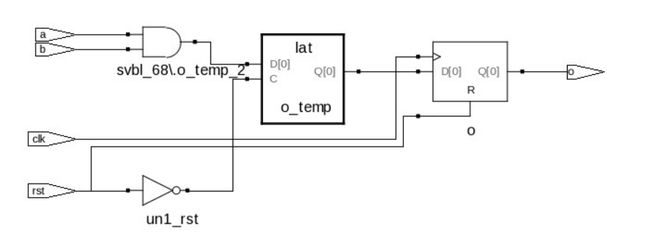
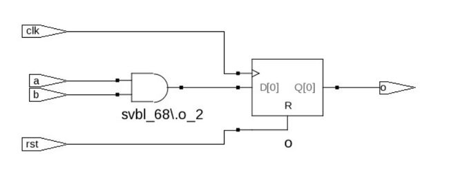
20、Which one is the correct circuit after synthesis for below Verilog code?
always@(posedge clk or posedge rst) begin
if(rst) begin
o <= 1’b0;
end else begin
o <= a && b;
end
end
正确答案:B
21、If you want to design an asynchronous FIFO with a dual port RAM. The FIFO width is 32bit, the depth is 16. If you can only use 4bit read/write address width, which kind of read/write address encoding is best?
Abinary coded decimal code
Bgrey code
Cone hot code
Dnone of above
正确答案:B
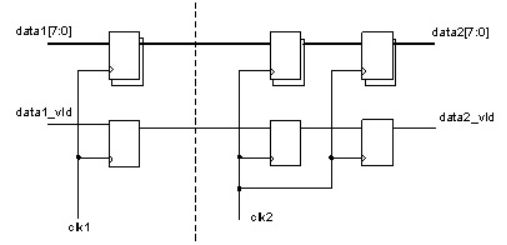
2The following figure is one async design. The data1_vld signal has enough pulse width and the data1[7:0] value will be kept unchanged within the pulse to assure we can get the data and one cycle pulse in clk2 domain. What problem do you see?
AIt is not necessary to synchronize data2[7:0].
Bdata2_vld is not a one cycle pulse.
Cdata2[7:0] and data2_vld do not need two flops to be synchronized to clk2 domain.
DI don’t see any problem.
正确答案:A
23Use a look-up table to design a FSM. The FSM has 25 states totally and 5 input control signals, what is the min size of look-up table to implement the FSM?
Athe look-up table is 30-bit address, 8-bit data
Bthe look-up table is 10-bit address, 5-bit data
Cthe look-up table is 10-bit address, 10-bit data
Dthe look-up table is 30-bit address, 5-bit data
正确答案:B
24Which one of below statements is correct?
AFPGA is a logic device using Product-Term structure
BThere’s no difference to connect the global clock to any FPGA user IO
C4 port input Look-up-table(LUT) can be implemented by 16x1 RAM
DFPGA device which use SRAM technology do not need to be configured after power on
正确答案:C
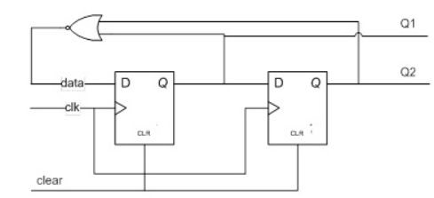
25、In below circuit, clk is 10MHz. Suppose clear signal is synchronous with clk. When 1s after release clear signal, what’s the output of [Q2, Q1]?
A[00]
B[01]
C[10]
D[11]
正确答案:C
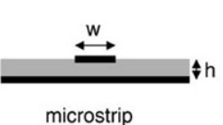
1、Which of the following methods would increase the characteristic impedance of a microstrip line?
(1) Increase height of dielectric substrate h
(2) Decrease height of dielectric substrate h
(3) Increase trace width w
(4) Decrease trace width w
(5) Reduce permittivity of the substrate
(6) Increase permittivity of the substrate
A(2)(4)(5)
B(1)(3)(6)
C(1)(3)(5)
D(1)(4)(5)
正确答案:D
2、If there is a signal with rise time 50 psec transmitting through an interconnector, and the 3dB bandwidth of the interconnector is 7GHz, how much is the rise time of the transmitted signal? (T rise time=0.35/BW)
A100 psec
B83.5 psec
C70.7 psec
D50.6 psec
正确答案:C
3、 Which expression is correct about crosstalk?
(1). The far-end crosstalk could be reduced by increasing the spacing between the signal traces.
(2). The total time the near-end noise lasts is 2 x TD. (TD: The time delay of the coupled) lines)
(3). The total time the near-end noise lasts is TD.
(4). No far-end crosstalk appears until a TD after the signal is launched.
(5). No far-end crosstalk appears until a 2 x TD after the signal is launched.
A(1)(2)(4)
B(1)(3)(5)
C(2)(4)
D(3)(5)
正确答案:A
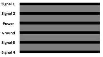
4、 If you have a 6 layers stackup as below, Which layer is the best for high speed signal layout considering signal integrity and EMC?
A Signal 1
B Signal 2
C Signal 3
D Signal 4
正确答案:C
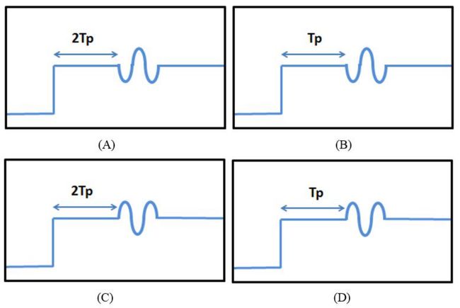
5、The impedance of the channel could be measured by TDR (time domain reflectometer). Now there is a channel including transmission line, capacity and inductor. Which waveform will you see in the TDR?
正确答案:C
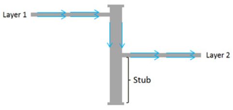
6、If there is a signal transmitting from one layer to anther through via as shown in Figure (a), you will see a sharp dip at 10GHz from the measured insertion loss result shown in Figure (b). Please estimate the length of the stub?
A7.5mm
B10mm
C15mm
D30mm
正确答案:A
7、 Compare the transmission velocity in microstrip (v1), buried microstrip (v2) and stripline (v3) which have the same dielectric constant. Which relationship bellow is correct?
A v1=v2=v3
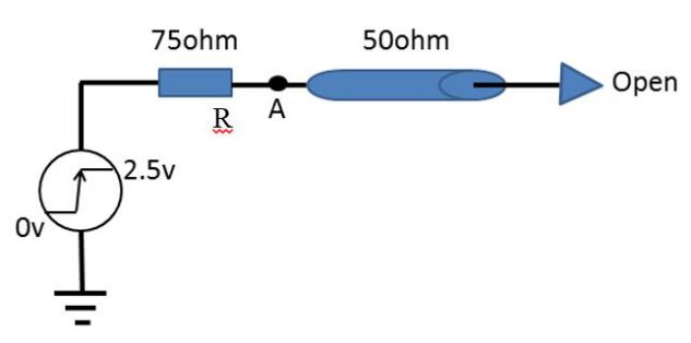
B v1 C v1>v2>v3 D v1>v3>v2 正确答案:C 8 (33/40) The coupled lines have the odd-mode impedance (Zodd), even-mode impedance (Zeven), differential impedance (Zdiff) and common impedance (Zcomn). Which relationship is right? A Zodd=Zdiff,Zeven=Zcomn B Zodd=Zdiff/2,Zeven=2*Zcomn C Zodd=2*Zdiff, Zeven=Zcomn/2 D Zodd=Zdiff/2, Zeven=Zcomn/2 正确答案:B 9、 Which is the best layout for discrete decoupling caps of dc power? 正确答案:B 10、The bellow figure is transmission line circuit. The time needed to transmit through the line is T. What is the voltage of point A at t=2T? A 2.5v B 2V C 1.2V D 2.2V 正确答案:B 11、 Which one or more of the followings properly describes random jitters: A exhibits Gaussian distribution B is a part of deterministic jitter C is linearly additive D is characterized by its bounded, peak-to-peak value 正确答案:A 12、 Choose WRONG approach about how to reduce probe to affect your measurement A Use a probe with higher impedance B Probe the signal somewhere else in the circuit at a test Point that has lower impedance. C Choose a probe with bigger tip cap parameter D Choose a probe with 5 time bandwidth than measured signal 正确答案:C 13、The inductance per unit length and capacitance per unit length of a lossless transmission line are 0.405nH and 0.2pF respectively. What is the characteristic impedance of this transmission line? A 40ohm B 45ohm C 50ohm D 55ohm 正确答案:B 14、 Which of the following factors determine the bandwidth of signal? A rise time B cycle time C clock jitter D flight time 正确答案:A 15、In multilayer board, through hole via structure NOT include: A Pad in positive layer B Pastemask in outer layer C Thermal pad or anti-pad in negative layer D Drill hole and plated wall of hole 正确答案:B
