C8051F310 模拟C2协议浅析与实现
C2
C2协议标准
- Each C2 frame is initiated with a START condition
- Each C2 frame terminates with a STOP condition
- All C2 devices include an 8-bit Device ID register and an 8-bit Revision ID register
寄存器
ADDRESS: Address Register
- 1.ADDRESS selects which C2 Data register is accessed during C2 Data Read/Write frames.
- 2.During Address Read frames, ADDRESS provides PI status information.
The Address Read command returns an 8-bit status code
| Bit | Name | Description |
|---|---|---|
| 7 | EBusy or FLBusy | This bit indicates when the EPROM or Flash is busy completing an operation. |
| 6 | EError | This bit is set to 1 when the EPROM encounters an error. |
| 5:2 | — | Unused |
| 1 | InBusy | This bit is set to 1 by the C2 Interface following a write to FPDAT. It is cleared to 0 when the PI acknowledges the write to FPDAT. |
| 0 | OutReady | This bit is set to 1 by the PI when output data is available in the FPDAT regis-ter. |
DEVICEID: Device ID Register
The Device ID register (DEVICEID) is a read-only C2 Data register containing the 8-bit device identifier of the target C2 device. The C2 address for register DEVICEID is 0x00
REVID: Revision ID Register
The Revision ID register (REVID) is a read-only C2 Data register containing the 8-bit revision identifier of the target C2 device. The C2 address for register REVID is 0x01
Data Register 0 ~ Data Register M-1
Revision ID (REVID)
Device ID (DEVICEID)
ADDRESS
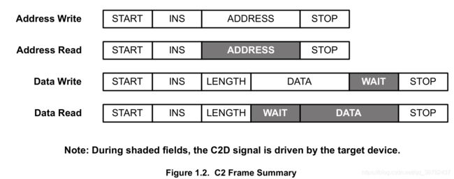
帧 C2 Instruction Frames
| Instruction | INS Code |
|---|---|
| Data Read | 00b |
| Address Read | 1 |
| Data Write | 01b |
| Address Write | 11b |
查看Table 1.3. C2 Bit Field Descriptions
此表讲述了有关于帧 的详细内容。
Address Read Frame

This instruction is typically used to quickly access status information。
Address Write Frame

An Address Write frame loads the target Address register。
Data Write Frame

A Data Write frame writes a specified value to the target Data register, as selected by the target Address register.
DATA length in bytes = LENGTH + 1。
如果要传递的数据是一个字节。那么INS字段的值就应该是00b。
Data Read Frame

A Data Read frame reads the contents of the target Data register, as selected by the target Address register.
Address Write,
Address Read,
Data Write,
Data Read
- 两个CPU。
- MCU_master
- MCU_key
MCU_master模拟C2协议给MCU_key烧写程序。
C2 Timing Specifications 时序图
Device Reset Timing
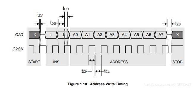
Address Write Timing
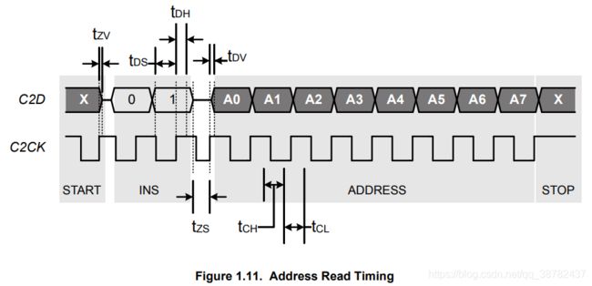
Address Read Timing
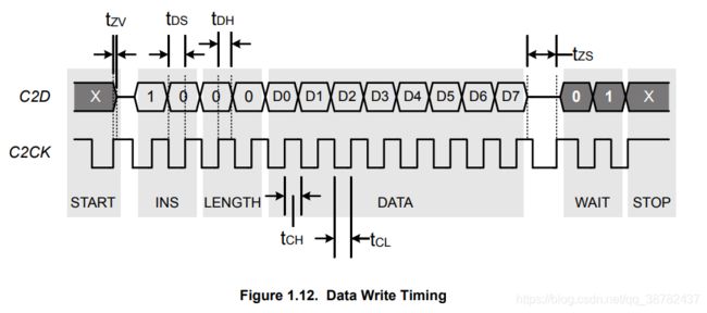
Data Write Timing
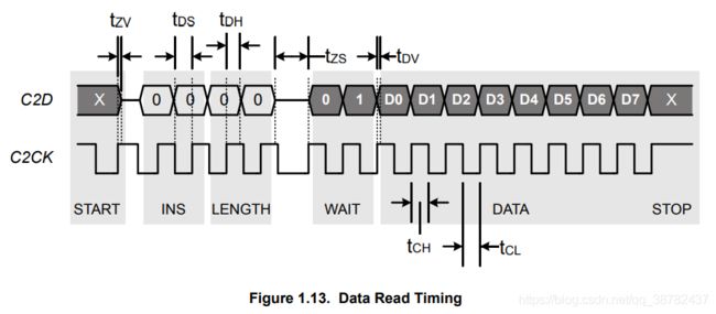
Data Read Timing
引脚分配
- MCU_master
P0.7  - MCU_C2CK2  - C2CK
P1.0  - MCU_C2DAT2 - C2D
需要注意的事项
- 1.If the C2CK master is an MCU, care should be taken to disable interrupts while C2CK is low in order to prevent a clock low time extending beyond 5 μs and potentially causing a target device reset.
C2相应的操作
增加了一个设备的开关操作。对于MCU_master而言需要传送数据显然需要将其引脚设置为push pull
void C2CK_DriverOn(void){ P0MDOUT |= 0x80; }// P0 ^ 7 push pull
void C2CK_DriverOff(void){
    P0 |= 0x80;         // P0 ^ 7 set 1
    P0MDOUT &= (~0x80); // set P0^7 out  open-drain
    }
void C2D_DriverOn(void){
	P1MDOUT |= 0x01;
}
void C2D_DriverOff(void){
	P1 |= 0x01;
  	P1MDOUT &= (~0x01);
}
开启引脚就是将其设置为强推。关闭就是将其设置为开漏。没有驱动能力。
Device Reset
To generate the reset timing:
- Turn the C2CK driver on.
- Force C2CK low.
- Wait at least 20 μs.
- Force C2CK high.
- Wait at least 2 μs.
- (Optional) Turn the C2CK driver off.
SetC2CK 高电平时一个下降沿保持最少tRD的时间然后一个上升沿。
  SetC2CK(LOW);
  Delay_us(20);
  SetC2CK(HIGH);
C2CK Clock Strobes
To generate C2CK clock strobes with a microcontroller-based programmer:
- Turn the C2CK driver on.
- Wait at least 40 ns. This helps ensure C2D data setup time.
- Force C2CK low. Ensure interrupts are disabled at this point.
- Wait between 80 and 5000 ns.
- Force C2CK high.
- Wait at least 120 ns. This helps ensure C2D data valid time.
void StrobeC2CK(void)
{
  SetC2CK(LOW);
  SetC2CK(HIGH);
}
注意 这里没有实现第一个步骤
因此调用StrobeC2CK之前需要确定C2CK为高电平
Performing the Address Write Instruction
The C2CK strobes mentioned in this section refer to the steps described in 1.5.2 C2CK Clock Strobes. To write to a target device’s ADDRESS register:
- Disable interrupts.
- Turn the C2CK driver on.
- Strobe C2CK. This will generate the START field and forces the C2D pin on the target device to become an input.
- Turn on the C2D driver.
- Force C2D high. This sets C2D for the 2-bit INS field, and the Address Write instruction is 11b.
- Strobe C2CK. This transfers the first bit of the INS field.
- Strobe C2CK. This transfers the second bit of the INS field.
- Force C2D to each bit of the address value being written to ADDRESS (starting with bit 0) and strobe C2CK for each bit.
- Turn off the C2D driver. This prepares C2D to possibly become an output from the target device.
- Strobe C2CK to generate the STOP field.
- (Optional) Turn off the C2CK driver.
- Re-enable interrupts.
void C2_WriteAR(unsigned char addr)
{
	static bit EA_SAVE = EA;
	EA = 0;
	C2CK_DriverOn();
	StrobeC2CK();
	C2D_DriverOn();
	SetC2D(HIGH);
	StrobeC2CK();
	//SetC2D(HIGH);  不确定需不需要再次实现C2D拉高 先保留着看一看
	StrobeC2CK();
	for (i = 0; i < 8; i++){
    SetC2D(addr & 0x01);
    StrobeC2CK();
    addr >>= 1;}  //发送每个字节 注意先发送低字节。
	C2D_DriverOff();
	// STOP field
  	StrobeC2CK();
  	C2CK_DriverOff();
  	EA = EA_SAVE;
}
解释
看了9号步骤才发现为什么在C2D_DriverOff以及C2CK_DriverOff为什么还需要将引脚从推挽设置为开漏。此时应该是需要接受来自target device输入。若是设置为推挽,那么target device就没有能力将引脚拉低,表示不了低电平。
Performing the Address Read Instruction
To read the status code from a target device’s ADDRESS register:
- Disable interrupts.
- Turn the C2CK driver on.
- Strobe C2CK. This will generate the START field and forces the C2D pin on the target device to become an input.
- Turn on the C2D driver.
- Force C2D low. This sets C2D for the first part of the 2-bit INS field, and the Address Read instruction is 01b.
- Strobe C2CK. This transfers the first bit of the INS field.
- Force C2D high. This sets C2D for the second part of the 2-bit INS field.
- Strobe C2CK. This transfers the second bit of the INS field.
- Turn off the C2D driver. This prepares C2D to become an output from the target device.
- Strobe C2CK and read C2D from the target device. The device will return the 8-bit status code returned from an Address Read instruction bit by bit starting with bit 0. C2CK must be strobed after each read of C2D.
- Strobe C2CK to generate the STOP field.
- (Optional) Turn off the C2CK driver.
- Re-enable interrupts.
基本和地址写指令区别不大,就是关闭中断然后引脚的设置
unsigned char C2_ReadAR(void)
{
	static bit EA_SAVE = EA;
	EA = 0;
	C2CK_DriverOn();
	// START field
	StrobeC2CK();
	C2D_DriverOn();
	//This sets C2D for the first part of the 2-bit INS field, and the Address Read instruction is 01b.
	SetC2D(LOW);
	//This transfers the first bit of the INS field.
	StrobeC2CK();
	This sets C2D for the second part of the 2-bit INS field.
	SetC2D(HIGH);
	// This transfers the second bit of the INS field.
	StrobeC2CK();
	C2D_DriverOff();
	for (i = 0; i < 8; i++){
    addr >>= 1;StrobeC2CK();
    if (GetC2D()) {addr |= 0x80;}  // 先接受bit0
    //STOP field.
    StrobeC2CK();
    C2CK_DriverOff();
    EA = EA_SAVE;
    return addr;
}
Performing the Data Write Instruction
- Disable interrupts.
- Turn on the C2CK driver.
- Strobe C2CK. This will generate the START field and forces the C2D pin on the target device to become an input.
- Turn on the C2D driver.
- Force C2D high. This sets C2D for the first part of the 2-bit INS field, and the Data Write instruction is 10b.
- Strobe C2CK. This transfers the first bit of the INS field.
- Force C2D low. This sets C2D for the second part of the 2-bit INS field.
- Strobe C2CK. This transfers the second bit of the INS field.
- Leave C2D low. This is the start of the LENGTH field, which will be 00b in this example.
- Strobe C2CK to start the LENGTH field.
- Strobe C2CK to finish transferring the LENGTH field.
- Force C2D to each bit of the data value being written to the data register (starting with bit 0) and strobe C2CK for each bit.
- Turn off the C2D driver. This prepares C2D to become an output from the target device.
- Srobe C2CK.
- Check C2D for a value of 1b. If C2D becomes 1, the WAIT field is over, as it can contain zero or more 0’s and exactly one 1b. If
C2D is not 1b, strobe C2CK and check the status again. - At this point, C2D is driving a 1, indicating the end of the WAIT field. Strobe C2CK to generate the STOP field.
- (Optional) Turn off the C2CK driver.
- Re-enable interrupts.
void C2_WriteDR(unsigned char dat)
{
  unsigned char i;
  static bit EA_SAVE;
  EA_SAVE = EA;
  EA = 0;
  // START field
  C2CK_DriverOn();
  StrobeC2CK();
  // INS field (01b, LSB first)
  C2D_DriverOn();
  SetC2D(HIGH);
  StrobeC2CK();
  SetC2D(LOW);
  StrobeC2CK();
  // LENGTH field (00b -> 1 byte)
  SetC2D(LOW);
  StrobeC2CK();
  SetC2D(LOW);
  StrobeC2CK();
  // DATA field
  for (i = 0; i < 8; i++)
  {
    SetC2D(dat & 0x01);
    StrobeC2CK();
    dat >>= 1;
  }
  C2D_DriverOff();
  // WAIT field
  do
  {
    StrobeC2CK();
  } while (!GetC2D());
  // STOP field
  StrobeC2CK();
  C2CK_DriverOff();

  EA = EA_SAVE;
}
Performing the Data Read Instruction
- Disable interrupts.
- Turn on the C2CK driver.
- Strobe C2CK. This will generate the START field and forces the C2D pin on the target device to become an input.
- Turn on the C2D driver.
- Force C2D low. This sets C2D for the first part of the 2-bit INS field, and the Data Read instruction is 00b.
- Strobe C2CK to transfer the first bit of the INS field.
- Strobe C2CK to transfer the second bit of the INS field.
- Leave C2D low. This is the start of the LENGTH field, which will be 00b in this example.
- Strobe C2CK to start the LENGTH field.
- Strobe C2CK to finish transferring the LENGTH field.
- Turn off the C2D driver. This prepares C2D to become an output from the target device.
- Strobe C2CK.
- Check C2D for a value of 1b. If C2D becomes 1, the WAIT field is over, as it can contain zero or more 0’s and exactly one 1b. If
C2D is not 1b, strobe C2CK and check the status again. - At this point, C2D is driving a 1, indicating the end of the WAIT field.
15.Strobe C2CK and read C2D from the target device. The device will return the contents of the data register bit by bit starting with bit - C2CK must be strobed after each read of C2D.
- Strobe C2CK to generate the STOP field.
- (Optional) Turn off the C2CK driver.
- Re-enable interrupts.
unsigned char C2_ReadDR(void)
{
  unsigned char i;
  unsigned char dat;
  static bit EA_SAVE;
  EA_SAVE = EA;
  EA = 0;
  // START field
  C2CK_DriverOn();
  StrobeC2CK();
  // INS field (00b, LSB first)
  C2D_DriverOn();
  SetC2D(LOW);
  StrobeC2CK();
  SetC2D(LOW);
  StrobeC2CK();
  // LENGTH field (00b -> 1 byte)
  SetC2D(LOW);
  StrobeC2CK();
  SetC2D(LOW);
  StrobeC2CK();
  C2D_DriverOff();
  // WAIT field
  do
  {
    StrobeC2CK();
  } while (!GetC2D());
  // DATA field
  dat = 0;
  for (i = 0; i < 8; i++)
  {
    dat >>= 1;
    StrobeC2CK();
    if (GetC2D())
      dat |= 0x80;
  }
  // STOP field
  StrobeC2CK();
  C2CK_DriverOff();

  EA = EA_SAVE;
  return dat;
}
Programming Registers
- FPCTL: Flash Programming Control Register
- FPDAT: Flash Programming Data Register
- EPCTL: EPROM Programming Control Register
- EPDAT: EPROM Programming Data Register
- EPADDRH and EPADDRL: EPROM Programming Address
- EPSTAT: EPROM Programming Status
其他
C2 isolation circuitry
参考资料
Markdown使用技巧总结——字体,颜色,字号,背景,首行缩进等
C2 协议标准手册
CSDN-markdown 扩展教程
