S3C2440 LCD控制器的设置
目录
- LCD 控制器
-
- LCDCON1的设置
- LCDCON2的设置
- LCDCON3的设置
- LCDCON4的设置
- LCDCON5的设置
- FRAME BUFFER START ADDRESS REGISTER
-
- LCDSADDR1的设置
- LCDSADDR2的设置
- LCDSADDR3的设置
- Lookup Table Register
-
- REDLUT的设置
- GREENLUT的设置
- BLUELUT的设置
- Dithering Mode Register
-
- DITHMODE的设置
- Temp Palette Register
-
- TPAL的设置
- LCD 中断寄存器
-
- LCDINTPND的设置
- LCDSRCPND的设置
- LCDINTMSK的设置
- TCON Control Register
-
- TCONSEL的设置
本文是基于韦东山视频的学习笔记
汇总点这
用液晶屏为4.3寸的 AT043TN24 V.1
LCD 控制器
LCDCON1的设置
[0X4D000000] LCDCON1 = 0x00000000 (初始值)
可读可写,应取 (9<<8) | (3<<5) | (0X0C<<1)
-
[27:18]LCDCON1: Provide the status of the line counter. Down count from LINEVAL to 0 -
- 是(read only),先不管
-
[17:8]CLKVAL: Determine the rates of VCLK and CLKVAL[9:0].
STN: VCLK = HCLK / (CLKVAL x 2) ( CLKVAL ≥2 )
TFT: VCLK = HCLK / [(CLKVAL+1) x 2] ( CLKVAL ≥ 0 ) -
- 我们是TFT屏,VCLK需要看LCD手册,手册里Clock cycle最小为5Mhz,最大为12Mhz,典型值为9Mhz
HCLK需要看内核内存时钟,为100Mhz
那我们就利用公式 5Mhz = 100Mhz / [(CLKVAL+1) x 2] 算出 CLKVAL 应等于 9
- 我们是TFT屏,VCLK需要看LCD手册,手册里Clock cycle最小为5Mhz,最大为12Mhz,典型值为9Mhz
-
[7]MMODE: Determine the toggle rate of the VM.
0 = Each Frame 1 = The rate defined by the MVAL -
- 这个东西没关系
-
[6:5]PNRMODE: Select the display mode.
00 = 4-bit dual scan display mode (STN)
01 = 4-bit single scan display mode (STN)
10 = 8-bit single scan display mode (STN)
11 = TFT LCD panel -
- TFT LCD,选 0b11
-
[4:1]BPPMODE: Select the BPP (Bits Per Pixel) mode.
0000 = 1 bpp for STN, Monochrome mode
0001 = 2 bpp for STN, 4-level gray mode
0010 = 4 bpp for STN, 16-level gray mode
0011 = 8 bpp for STN, color mode (256 color)
0100 = packed 12 bpp for STN, color mode (4096 color)
0101 = unpacked 12 bpp for STN, color mode (4096 color)
0110 = 16 bpp for STN, color mode (4096 color)
1000 = 1 bpp for TFT
1001 = 2 bpp for TFT
1010 = 4 bpp for TFT
1011 = 8 bpp for TFT
1100 = 16 bpp for TFT
1101 = 24 bpp for TFT -
- 我们为16 bpp ,所以是 0b1100
-
[0]ENVID: LCD video output and the logic enable/disable.
0 = Disable the video output and the LCD control signal.
1 = Enable the video output and the LCD control signal. -
- LCD 使能引脚,现在是设置先不使能,取0
LCDCON2的设置
寄存器地址:0X4D000004,可读可写,初始化值:0x00000000, 应取
这个寄存器对应的是这一帧的图
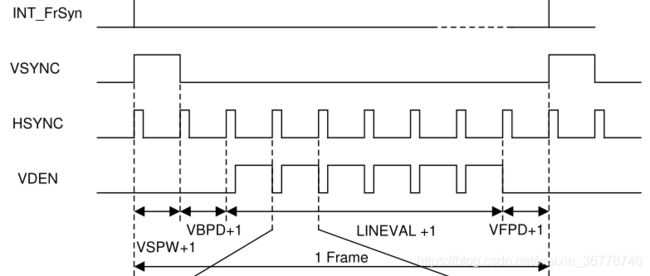
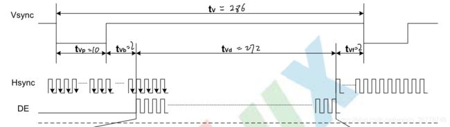
LCD都是从左上到右下扫描显示, 一个画面扫描完,VSYNC(垂直同步信号)就会发出,LCD就会开始重新扫描,而 VSYNC 的发出有一定的时间限制,这个需要结合LCD手册
[31:24]VBPD:
TFT: Vertical back porch is the number of inactive lines at the start of a frame, after vertical synchronization period.
STN: These bits should be set to zero on STN LCD-
- TFT,垂直方向的时间参数,脉冲消失要到多长才可以下一行的数据开始,结合手册是1
[23:14]LINEVAL: TFT/STN: These bits determine the vertical size of LCD panel.-
- 结合手册这里是271
[13:6]VFPD:
TFT: Vertical front porch is the number of inactive lines at the end of a frame, before vertical synchronization period.
STN: These bits should be set to zero on STN LCD.-
- 一行扫描完要多久才到下一行,结合手册是1
[5:0]VSPW:
TFT: Vertical sync pulse width determines the VSYNC pulse's high level width by counting the number of inactive lines.
STN: These bits should be set to zero on STN LCD.-
- 结合手册知道这里为9
LCDCON3的设置
寄存器地址:0X4D000008,可读可写,初始化值:0x00000000
需要结合这一图片
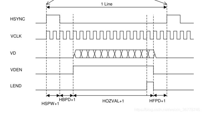
结合LCD手册

[25:19] HBPD (TFT) / WDLY (STN):
TFT: Horizontal back porch is the number of VCLK periods between the falling edge of HSYNC and the start of active data.
STN: WDLY[1:0] bits determine the delay between VLINE and VCLK by counting the number of the HCLK. WDLY[7:2] are reserved.
00 = 16 HCLK, 01 = 32 HCLK, 10 = 48 HCLK, 11 = 64 HCLK-
- 结合手册 HBPD 等于1
[18:8]HOZVAL: TFT/STN: These bits determine the horizontal size of LCD panel.
HOZVAL has to be determined to meet the condition that total bytes of 1 line are 4n bytes. If the x size of LCD is 120 dot in mono mode, x=120 cannot be supported because 1 line consists of 15 bytes. Instead, x=128 in mono mode can be supported because 1 line is composed of 16 bytes (2n). LCD panel driver will discard the additional 8 dot.-
- 结合手册得 HOZVAL 等于479
[7:0] HFPD (TFT) / LINEBLANK (STN):
TFT: Horizontal front porch is the number of VCLK periods between the end of active data and the rising edge of HSYNC.
STN: These bits indicate the blank time in one horizontal line duration time. These bits adjust the rate of the VLINE finely.
The unit of LINEBLANK is HCLK x 8. Ex) If the value of LINEBLANK is 10, the blank time is inserted to VCLK during 80 HCLK.-
- 结合手册得 **HFPD ** 等于1
LCDCON4的设置
寄存器地址:0X4D00000C,可读可写,初始化值:0x00000000
[15:8] MVAL: STN: These bit define the rate at which the VM signal will toggle if the MMODE bit is set to logic '1'.-
- 不管事,不用管
[7:0] HSPW(TFT) / WLH(STN):
TFT: Horizontal sync pulse width determines the HSYNC pulse's high level width by counting the number of the VCLK.
STN: WLH[1:0] bits determine the VLINE pulse's high level width by counting the number of the HCLK. WLH[7:2] are reserved
00 = 16 HCLK, 01 = 32 HCLK, 10 = 48 HCLK, 11 = 64 HCLK-
- 结合手册得 HSPW 等于40
LCDCON5的设置
寄存器地址:0X4D000010,可读可写,初始化值:0x00000000,可设置为0xB41
[31:17] Reserved: This bit is reserved and the value should be ‘0’.[16:15] VSTATUS: TFT: Vertical Status (read only).
00 = VSYNC 01 = BACK Porch
10 = ACTIVE 11 = FRONT Porch-
- 只读
[14:13] HSTATUS: TFT: Horizontal Status (read only).
00 = HSYNC 01 = BACK Porch
10 = ACTIVE 11 = FRONT Porch-
- 只读
[12] BPP24BL: TFT: This bit determines the order of 24 bpp video memory.
0 = LSB valid 1 = MSB Valid-
- 24位的,我们16位,不管
[11] FRM565: TFT: This bit selects the format of 16 bpp output video data.
0 = 5:5:5:1 Format 1 = 5:6:5 Format-
- 565格式,设置为1
[10] INVVCLK: STN/TFT: This bit controls the polarity of the VCLK active edge.
0 = The video data is fetched at VCLK falling edge
1 = The video data is fetched at VCLK rising edge-
- LCD手册里是下降沿取数据,设置为0
[9] INVVLINE: STN/TFT: This bit indicates the VLINE/HSYNC pulse polarity.
0 = Normal 1 = Inverted-
- LCD手册和 S3C2440 里的手册相反,选1
[8] INVVFRAME: STN/TFT: This bit indicates the VFRAME/VSYNC pulse polarity.
0 = Normal 1 = Inverted-
- 同样,相反,选1
[7] INVVD: STN/TFT: This bit indicates the VD (video data) pulse polarity.
0 = Normal 1 = VD is inverted.-
- 相同,选0
[6] INVVDEN: TFT: This bit indicates the VDEN signal polarity.
0 = normal 1 = inverted-
- 相同,选1
[5] INVPWREN: STN/TFT: This bit indicates the PWREN signal polarity.
0 = normal 1 = inverted-
- 不知道什么,选0
[4] INVLEND: TFT: This bit indicates the LEND signal polarity.
0 = normal 1 = inverted-
- 选0
[3] PWREN: STN/TFT: LCD_PWREN output signal enable/disable.
0 = Disable PWREN signal 1 = Enable PWREN signal-
- 选0
[2] ENLEND: TFT: LEND output signal enable/disable
0 = Disable LEND signal 1 = Enable LEND signal-
- 使能LCD,先设置为0
[1] BSWP: STN/TFT: Byte swap control bit.
0 = Swap Disable 1 = Swap Enable-
- 选0,BSWP 和 HWSWP 为[0:1] 时,数据从低到高存放
[0] HWSWP: STN/TFT: Half-Word swap control bit
0 = Swap Disable 1 = Swap Enable-
- 选1,BSWP 和 HWSWP 为[0:1] 时,数据从低到高存放
FRAME BUFFER START ADDRESS REGISTER
LCDSADDR1的设置
STN/TFT: Frame buffer start address 1 register,寄存器地址:0X4D000014,可读可写,初始化值:0x00000000
[29:21] LCDBANK: These bits indicate A[30:22] of the bank location for the video buffer in the system memory. LCDBANK value cannot be changed even when moving the view port. LCD frame buffer should be within aligned 4MB region, which ensures that LCDBANK value will not be changed when moving the view port. So, care should be taken to use the malloc() function.-
- 显存地址
[20:0] LCDBASEU:
For dual-scan LCD : These bits indicate A[21:1] of the start address of the upper address counter, which is for the upper frame memory of dual scan LCD or the frame memory of single scan LCD.
For single-scan LCD : These bits indicate A[21:1] of the start address of the LCD frame buffer.-
- 显存地址
LCDSADDR2的设置
STN/TFT: Frame buffer start address 1 register,寄存器地址:0X4D000014,可读可写,初始化值:0x00000000
[20:0] LCDBASEL:
For dual-scan LCD: These bits indicate A[21:1] of the start address of the lower address counter, which is used for the lower frame memory of dual scan LCD.
For single scan LCD: These bits indicate A[21:1] of the end address of the LCD frame buffer.
LCDBASEL = ((the frame end address) >>1) + 1 = LCDBASEU + (PAGEWIDTH+OFFSIZE) x (LINEVAL+1)
LCDSADDR3的设置
STN/TFT: Virtual screen address set,寄存器地址:0X4D00001C,可读可写,初始化值:0x00000000
[21:11] OFFSIZE: Virtual screen offset size (the number of half words).
This value defines the difference between the address of the last half word displayed on the previous LCD line and the address of the first half word to be displayed in the new LCD line.-
- 虚拟偏移地址,设为0
[10:0] PAGEWIDTH: Virtual screen page width (the number of half words).
This value defines the width of the view port in the frame.-
- 以2字节长度为单位表示一行的长度,即为 480 * 16 /16
NOTE: The values of PAGEWIDTH and OFFSIZE must be changed when ENVID bit is 0.
- Example 1. LCD panel = 320 x 240, 16gray, single scan
Frame start address = 0x0c500000
Offset dot number = 2048 dots ( 512 half words )
LINEVAL = 240-1 = 0xef
PAGEWIDTH = 320 x 4 / 16 = 0x50
OFFSIZE = 512 = 0x200
LCDBANK = 0x0c500000 >> 22 = 0x31
LCDBASEU = 0x100000 >> 1 = 0x80000
LCDBASEL = 0x80000 + ( 0x50 + 0x200 ) x ( 0xef + 1 ) = 0xa2b00- Example 2. LCD panel = 320 x 240, 16gray, dual scan
Frame start address = 0x0c500000
Offset dot number = 2048 dots ( 512 half words )
LINEVAL = 120-1 = 0x77
PAGEWIDTH = 320 x 4 / 16 = 0x50
OFFSIZE = 512 = 0x200
LCDBANK = 0x0c500000 >> 22 = 0x31
LCDBASEU = 0x100000 >> 1 = 0x80000
LCDBASEL = 0x80000 + ( 0x50 + 0x200 ) x ( 0x77 + 1 ) = 0x91580- Example 3. LCD panel = 320*240, color, single scan
Frame start address = 0x0c500000
Offset dot number = 1024 dots ( 512 half words )
LINEVAL = 240-1 = 0xef
PAGEWIDTH = 320 x 8 / 16 = 0xa0
OFFSIZE = 512 = 0x200
LCDBANK = 0x0c500000 >> 22 = 0x31
LCDBASEU = 0x100000 >> 1 = 0x80000
LCDBASEL = 0x80000 + ( 0xa0 + 0x200 ) x ( 0xef + 1 ) = 0xa7600
Lookup Table Register
REDLUT的设置
STN: Red lookup table register,寄存器地址:0X4D000020,可读可写,初始化值:0x00000000
[31:0] REDVAL: These bits define which of the 16 shades will be chosen by each of the 8 possible red combinations.
000 = REDVAL[3:0], 001 = REDVAL[7:4]
010 = REDVAL[11:8], 011 = REDVAL[15:12]
100 = REDVAL[19:16], 101 = REDVAL[23:20]
110 = REDVAL[27:24], 111 = REDVAL[31:28]-
- STN的设置器,不管
GREENLUT的设置
STN: Green lookup table register,寄存器地址:0X4D000024,可读可写,初始化值:0x00000000
[31:0] GREENVAL: These bits define which of the 16 shades will be chosen by each of the 8 possible green combinations.
000 = GREENVAL[3:0], 001 = GREENVAL[7:4]
010 = GREENVAL[11:8], 011 = GREENVAL[15:12]
100 = GREENVAL[19:16], 101 = GREENVAL[23:20]
110 = GREENVAL[27:24], 111 = GREENVAL[31:28]-
- STN的设置器,不管
BLUELUT的设置
STN: Blue lookup table register,寄存器地址:0X4D000028,可读可写,初始化值:0x00000000
[15:0] BLUEVAL: These bits define which of the 16 shades will be chosen by each of the 4 possible blue combinations.
00 = BLUEVAL[3:0], 01 = BLUEVAL[7:4]
10 = BLUEVAL[11:8], 11 = BLUEVAL[15:12]-
- STN的设置器,不管
Dithering Mode Register
DITHMODE的设置
STN: Dithering mode register. This register reset value is 0x00000 But, user can change this value to 0x12210. (Refer to a sample program source for the latest value of this register.),寄存器地址:0X4D00004C,可读可写,初始化值:0x00000000
[18:0] DITHMODE: Use one of following value for your LCD: 0x00000 or 0x12210-
- STN的设置器,不管
Temp Palette Register
TPAL的设置
TFT: Temporary palette register. This register value will be video data at next frame.,寄存器地址:0X4D000050,可读可写,初始化值:0x00000000
[24] TPALEN: Temporary palette register enable bit.
0 = Disable 1 = Enable-
- 临时调色板,先不用,为0
[23:0] TPALVAL: Temporary palette value register.
TPALVAL[23:16] : RED
TPALVAL[15:8] : GREEN
TPALVAL[7:0] : BLUE-
LCD 中断寄存器
LCDINTPND的设置
Indicate the LCD interrupt pending register.,寄存器地址:0X4D000054,可读可写,初始化值:0x00000000
[1] INT_FrSyn: LCD frame synchronized interrupt pending bit.
0 = The interrupt has not been requested.
1 = The frame has asserted the interrupt request-
- 不用中断
[0] INT_FiCnt: LCD FIFO interrupt pending bit.
0 = The interrupt has not been requested.
1 = LCD FIFO interrupt is requested when LCD FIFO reaches trigger level.-
- 不用中断
LCDSRCPND的设置
Indicate the LCD interrupt source pending register.,寄存器地址:0X4D000058,可读可写,初始化值:0x00000000
[1] INT_FrSyn: LCD frame synchronized interrupt source pending bit.
0 = The interrupt has not been requested.
1 = The frame has asserted the interrupt request.-
- 不用中断
[0] INT_FiCnt: LCD FIFO interrupt source pending bit.
0 = The interrupt has not been requested.
1 = LCD FIFO interrupt is requested when LCD FIFO reaches trigger level.-
- 不用中断
LCDINTMSK的设置
Determine which interrupt source is masked. The masked interrupt source will not be serviced..,寄存器地址:0X4D000058,可读可写,初始化值:0x3
[2] FIWSEL: Determine the trigger level of LCD FIFO.
0 = 4 words 1 = 8 words-
- 不用中断
[1] INT_FrSyn: Mask LCD frame synchronized interrupt.
0 = The interrupt service is available.
1 = The interrupt service is masked.-
- 不用中断
[0] INT_FiCnt: Mask LCD FIFO interrupt.
0 = The interrupt service is available.
1 = The interrupt service is masked.-
- 不用中断
TCON Control Register
TCONSEL的设置
This register controls the LPC3600/LCC3600 modes...,寄存器地址:0X4D000060,可读可写,初始化值:0xF84
-
[11] LCC_TEST2: LCC3600 Test Mode 2 ( Read Only ) -
[10] LCC_TEST1: LCC3600 Test Mode 1 ( Read Only ) -
[9] LCC_SEL5: Select STV polarity -
[8] LCC_SEL4: Select CPV signal pin 0 -
[7] LCC_SEL3: Select CPV signal pin 1 -
[6] LCC_SEL2: Select Line/Dot inversion -
[5] LCC_SEL1: Select DG/Normal mode -
[4] LCC_EN: Determine LCC3600 Enable/Disable
0 = LCC3600 Disable, 1 = LCC3600 Enable -
[3] CPV_SEL: Select CPV Pulse low width -
[2] MODE_SEL: Select DE/Sync mode
0 = Sync mode, 1 = DE mode -
[1] RES_SEL: Select output resolution type
0 = 320 x 240
1 = 240 x 320 -
[0]LPC_EN: Determine LPC3600 Enable/Disable
0 = LPC3600 Disable, 1 = LPC3600 Enable
NOTE: Both LPC_EN and LCC_EN enable is not permitted. Only one TCON can be enabled at the same time.