Changing the Output Voltage of a Switching Regulator on the Fly
http://www.powerguru.org/changing-the-output-voltage-of-a-switching-regulator-on-the-fly/
There are many different ways to change the output voltage
Applications that require the output voltage of a power supply to change dynamically come from a wide variety of areas. Examples are sensor applications that require a different supply voltage under varying circumstances and LED applications, where the DC current through an LED, needs to be reduced when the ambient temperature rises above a critical point - to name but a few possibilities.
By Frederik Dostal, National Semiconductor
This article discusses some methods of changing the output voltage of a power supply on the fly. It includes a “how to guide” as well as information on the frequency domain behavior of the control loop of such a system.
Digital Voltage Scaling
Digital voltage scaling (DVS) is becoming more and more important to reduce energy consumption in portable applications by adapting the supply voltage of DSPs and microcontrollers depending on the upcoming tasks. Power supplies for DVS applications are usually set up with VID pins which come with special power management ICs specifically designed for such applications. These VID pins controlled digitally and are used to change the reference voltage of the controller IC, generating a programmable output voltage.
Most switching regulators are not designed for specific microprocessor (DVS) applications so they do not allow modification of the internal reference. The only way to change the regulated output voltage is to modify the feedback pin circuitry.
In principle there are many different ways to change the output voltage by influencing the feedback pin. Three of the most important ways are mentioned in this article.
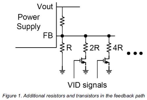
One basic way is to add an additional resistor in parallel or in series to the feedback resistors. To do this on the fly, transistors have to be used in the signal path and the signal controlling the output voltage will have to be able to turn the transistor on and off. Figure 1 shows additional resistor and transistors in the feedback path of a power supply to modify the output voltage.

Direct connection of Vcontrol to the feedback divider
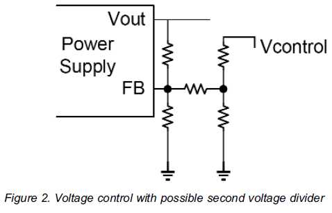
A second possibility is to use the voltage control signal and feed it through a second resistive voltage divider into the feedback pin. The output voltage can be set to multiple voltages and can be changed in continuous transitions and not just discretely as in the way described in the previous paragraph. Also, only one or two additional resistors are required, making this a low cost alternative. The downside of this method is that the programming voltage (Vcontrol) is rather restricted. The control signal will have to be able to drive the resistive dividers and every bit of this control voltage’s behavior is used by the FB pin to alter Vout in a purely analog manner.
Using an operational amplifier in the feedback path
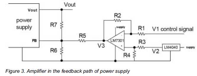
A very flexible way of influencing the feedback pin while not being so restricted in terms of the control signal is to use an operational amplifier. It can be used to inject some current into the feedback divider which then forces the control loop of the power supply to change the output voltage. This way the output voltage can be varied continuously as a function of the current injected into the feedback node.
Often, the information controlling the output voltage change on a power supply in sensor applications as well as motor drive applications is an analog signal. Depending on the nature of this control signal, the circuit around the operational amplifier can be defined to set the lowest voltage output independent of what the control signal range is. Also there is great flexibility in the ratio of control signal change to change in the output voltage.
Figure 3 shows an amplifier circuit in the feedback path of a switching power supply. The difference amplifier uses an operational amplifier and four additional resistors R1 through R4. The output of the operational amplifier acts like a voltage source. In order to inject a current into the feedback node this voltage is converted into a current by resistor R5. It equals the internal impedance of the current source which the operational amplifier and R5 constitute. Together with the feedback resistors R6 and R7 any output voltage changes can be set based on almost any given control signal.
The signal voltage V1 is the control signal. The voltage V2 is a reference voltage for the operational amplifier. It should be a fairly constant voltage since variations on it will change the output voltage of the power supply as well. If a fairly precise rail in the system is available it can generally be used. A good solution is a low voltage reference IC such as National Semiconductors LM4040.

Concerns of the operational amplifier
The operational amplifier needs a supply voltage that ensures proper operation at both ends of the output voltage range. Depending on what the specifications of the power supply are the amplifier may or may not be connected directly to Vin or Vout. In some designs, an amplifier with a wide supply range or an additional supply for the bias voltage of the amplifier might be needed. Since the current required for the supply rails of the amplifier is very little, often the supply is only a resistive divider with a zener diode to limit the supply rail. If amplifiers with a very wide input voltage range such as National Semiconductors LM7301 are used, in most applications they can be attached to the input or output voltage of a design directly. The LM7301 has an input voltage range from 1.8V up to 32V and is optimized to require only 600uA supply current.
Large signal behavior of the power supply
Building a power supply circuit with a varying output voltage is somewhat more difficult than with a fixed output voltage. The selection of the power path components does not only depend on the supply voltage and the output load but also on the output voltage. The usual extremes to look at in a fixed output voltage supply are Vin min, Vin max, Iout min and Iout max. With Vout changing also there is Vout min and Vout max to be considered as well. A spread sheet for the circuit design will be very helpful since there are quite a few combinations to look at.
Stability evaluation: PWM control and constant-on-time control power supplies
Regarding the control loop, it is very important to make sure that a power supply with a changing output voltage is stable under all output voltage conditions.
When using a voltage mode or current mode PWM switching regulator the feedback divider network has an effect on the gain of the control loop.
Buck regulators have a linear transfer function and the compensation will generally not have to be optimized for different output voltages. Other topologies such as the boost regulators do not have a linear transfer function and as such the optimization of the control loop will change when the output voltage or input voltage changes. When power supplies with a variable output voltage are designed, loop stability tests need to be performed throughout the whole output voltage range.
Another interesting observation is that there is a difference if the power supply’s output voltage is changed by modifying the low-side feedback resistor or by injecting a current into the feedback node. Changing the low-side feedback resistor will not change the gain of the circuit if the error amplifier is a conventional opamp. So a designer can replace the low-side feedback resistor with a potentiometer and change the output voltage of the power supply without changing the feedback gain. This will not be true if the error amplifier is a transconductance (gm) amp.
When current is injected into the feedback node with a current source with internal impedance such as the circuit in Figure 3, the frequency behavior of the system depends on the internal impedance of the current source (R5 in Figure 3) but not on the actual current injected into the feedback node. So the closed loop evaluation can be done once for a design with one fixed R5 without needing to redo it for every possible output voltage. However this only holds true for a buck type regulator where the plant gain is independent of duty cycle.
In constant-on-time control ICs such as National Semiconductor’s LM5010 which basically use a comparator at the feedback pin, stability is not a concern. The output voltage is controlled in a hysteretic window directly with some short propagation delay. It does not require compensation components or further stability measurements. The only thing to watch out for is the requirement that in such regulators there is always a bit of ripple voltage necessary on the feedback pin. If this minimum voltage ripple is not available, the hysteretic comparator’s thresholds are not cleanly crossed and the result is frequency jitter and erratic behavior. When a constant-on-time regulator is used for a variable output voltage design, the minimum and maximum ripple on the feedback pin has to be checked. There are techniques of introducing additional ripple on the feedback pin in such designs which can be taken from the individual datasheets of these ICs.
Changing the output voltage on the fly very suddenly
If the output voltage of a power supply is modified on the fly the effect is very similar to the input voltage changing with a fixed output voltage. The duty cycle will have to adapt to the new Vin to Vout ratio and the regulator will need to adjust to the new situation. Just as in input voltage changes the output might see some overshoot or delay in coming up. How fast the regulator can adapt to the new conditions and how much overshoot or delay one will observe is given by the bandwidth of the circuit. One thing that can cause surprises is in regulators that have built in output over voltage protection, a sudden reduction in the programmed output voltage can trip the OVP comparators and force the regulator to latch off. The solution with these types of regulators is to force the output voltage to move relatively slowly when moving lower.
There is no magic about it
Changing the output voltage of a power supply on the fly is not magic. There is nothing to be afraid of as long as all design aspects are considered carefully. Unfortunately changing Vout and making it a variable makes a power supply design more demanding.