常用的RS485芯片简介
本文将简单介绍常用RS485 芯片
MAX48x系列芯片
The MAX481, MAX483, MAX485, MAX487–MAX491, and MAX1487 are low-power transceivers for RS-485 and RS-422 communication. Each part contains one driver and onereceiver. The MAX483, MAX487, MAX488, and MAX489 feature reduced slew-rate drivers that minimize EMI and reduce reflections caused by improperly terminated cables,thus allowing error-free data transmission up to 250kbps.The driver slew rates of the MAX481, MAX485, MAX490,MAX491, and MAX1487 are not limited, allowing them to transmit up to 2.5Mbps.
These transceivers draw between 120µA and 500µA of supply current when unloaded or fully loaded with disabled drivers. Additionally, the MAX481, MAX483, and MAX487 have a low-current shutdown mode in which they consume only 0.1µA. All parts operate from a single 5V supply.
Drivers are short-circuit current limited and are protected against excessive power dissipation by thermal shutdown circuitry that places the driver outputs into a high-imped-ance state. The receiver input has a fail-safe feature that guarantees a logic-high output if the input is open circuit.
The MAX487 and MAX1487 feature quarter-unit-load
receiver input impedance, allowing up to 128 MAX487/
MAX1487 transceivers on the bus. Full-duplex communi-
cations are obtained using the MAX488–MAX491, while
the MAX481, MAX483, MAX485, MAX487, and MAX1487
are designed for half-duplex applications.
PIN 脚定义:
MAX308x 系列
The MAX3080–MAX3089 high-speed transceivers for RS-485/RS-422 communication contain one driver and one receiver. These devices feature fail-safe circuitry,which guarantees a logic-high receiver output when the receiver inputs are open or shorted. This means that the receiver output will be a logic high if all transmitters on a terminated bus are disabled (high impedance).
The MAX3080/MAX3081/MAX3082 feature reduced slew-rate drivers that minimize EMI and reduce reflec-tions caused by improperly terminated cables, allowing error-free data transmission up to 115kbps. The MAX3083/MAX3084/MAX3085 offer higher driver out-put slew-rate limits, allowing transmit speeds up to 500kbps. The MAX3086/MAX3087/MAX3088’s driverslew rates are not limited, making transmit speeds upto 10Mbps possible. The MAX3089’s slew rate isselectable between 115kbps, 500kbps, and 10Mbps by driving a selector pin with a single three-state driver.
These transceivers typically draw 375µA of supply current when unloaded, or when fully loaded with the drivers disabled.
All devices have a 1/8-unit-load receiver input impedance that allows up to 256 transceivers on the bus. The MAX3082/MAX3085/MAX3088 are intended for half-duplex communications, while the MAX3080/MAX3081/MAX3083/MAX3084/MAX3086/MAX3087 are intended for full-duplex communications. The MAX3089 is selectable between half-duplex and full-duplex operation. It
also features independently programmable receiver and transmitter output phase via separate pins.
Pin 脚定义:
MAX3443E
The MAX3443E fault-protected RS-485/RS-422 transceiver features ±60V protection from signal faults on communication bus lines. Each device contains one differential line driver with three-state output, and one differential line receiver with three-state input. The 1/4-unit-load receiver input impedance allows up to 128 transceivers on a single bus. The device operates from a 5V supply at data rates up to 10Mbps. True fail-safe inputs guarantee a logic-high receiver output when the receiver inputs are open, shorted, or connected to an idle data line.
Hot-swap circuitry eliminates false transitions on thedata cable during circuit initialization or connection to a live backplane. Short-circuit current limiting and thermal shutdown circuitry protect the driver against excessive power dissipation, and integrated ±15kV ESD protection eliminates costly external protection devices.
The MAX3443E is available in 8-pin SO and PDIP packages, and is specified over commercial, industrial, and automotive temperature ranges.
封装方式及工作环境温度列表
Pin脚定义:
华之美半导体Max485兼容芯片
是一款国产RS485芯片,应用于 RS-485 和 RS-422通信系统的收发芯片。MAX485 传输和接收的数据传输率可高达 2.5Mbps。485 为半双工型。另外,485 有驱动使能(DE)和接收使能(RE)管脚,当关闭时,驱动和接收输出为高阻。MAX485 具有失效保护功能,在处于接收状态时,输入端开路或短路接收器输出为高电平。
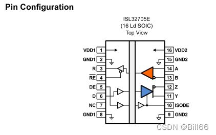
ISL32705E
The ISL32705E is a galvanically isolated, full-duplex differential bus transceiver, designed for bidirectional data transmission meeting the RS-485 and RS-422 standards for balanced communication. All bus terminals are protected against ±7kV ESD strikes without latch-up.
The device uses Giant Magnetoresistance (GMR) as isolation technology. A unique ceramic/polymer composite barrier provides excellent isolation and nearlyunlimited barrier life.
The part is available in a 16 Ld wide-body SOIC package providing true 8mm creepage distance.
The ISL32705E delivers a minimum of 1.5V into a 54Ω differential load for excellent data integrity over long cable lengths.
The device is compatible with 3V and 5V input supplies, allowing an interface to standard microcontrollers without additional level shifting.
Current limiting and thermal shutdown features protect against output short-circuits and bus contention that may cause excessive power dissipation. Receiver inputs feature a “fail-safe if open” design, ensuring a logic high R-output if A/B are floating.
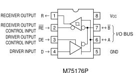
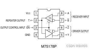
M7517xP 系列
Each of the M75176 to M75179 is a semiconductor IC with a built-in differential driver and a built-in differential receiver both of which meet the EIA standards RS-422A and RS-485.
The M75176P to M75179P are line interface ICs which meet EIA standards RS-422A and RS-485, and are suitable for long-distance, high-speed data transmission.
The M75176P is designed to connect the driver circuit output and the receiver input to each other internally, and serves as a line transceiver. The M75177P/M75178P is designed to connect the receiver circuit output and the driver circuit input internally, and serves as a line repeater. The M75177P and M75178P enter the output enabled state with active “H” and active “L”, respectively. The M75179P is equipped with abuilt-in differential driver and a built-in differential receiver. It does not have an output control input pin but its output im-pedance at the power-OFF time goes high.
Pin脚定义:
SN65HVD11-HT
The SN65HVD11 combines a 3-state differential line driver and differential input line receiver that operates with a single 3.3-V power supply. It is designed for balanced transmission lines and meets or exceeds ANSI TIA/EIA-485-A and ISO 8482:1993, with the exception that the thermal shutdown is removed. This differential bus transceiver is a monolithic integrated circuit designed for bidirectional data communication on multipoint bus-transmission lines. The driver and receiver have active-high and active-low enables, respectively, that can be externally connected together to function as direction control.
The driver differential outputs and receiver differential inputs connect internally to form a differential input/ output (I/O) bus port that is designed to offer minimum loading to the bus when the driver is disabled or V CC = 0.
Pin脚定义:
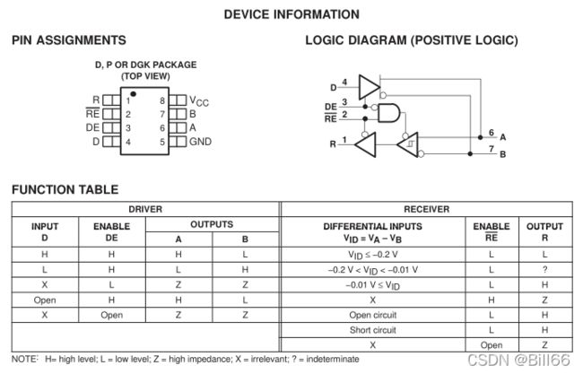
SN65HVD3082E/SN75HVD3082E
These devices are half-duplex transceivers designed for RS-485 data bus networks. Powered by a 5-V supply, they are fully compliant with TIA/EIA-485A standard. With controlled transition times, these devices are suitable for transmitting data over long twisted-pair cables.
SN65HVD3082E and SN75HVD3082E devices are optimized for signaling rates up to 200 kbps.
SN65HVD3085E is suitable for data transmission up to 1 Mbps, whereas SN65HVD3088E is suitable for applications requiring signaling rates up to 20 Mbps.These devices are designed to operate with very low supply current, typically 0.3 mA, exclusive of the load.When in the inactive shutdown mode, the supply current drops to a few nanoamps, making these devices ideal for
power-sensitive applications.
The wide common-mode range and high ESD protection levels of these devices make them suitable for demanding applications such as energy meter networks, electrical inverters, status/command signals across telecom racks,cabled chassis interconnects, and industrial automation networks where noise tolerance is essential. These devices match the industry-standard footprint of SN75176.Power-on reset circuits keep the outputs in a high-impedance state until the supply voltage has stabilized. A thermal shutdown function protects the device from
damage due to system fault conditions. The SN75HVD3082E is characterized for operation from 0°C to 70°C and SN65HVD308xE are characterized for operation from −40°C to 85°C air temperature.
SP3485
The SP3485 device is a +3.3V low power half-duplex transceiver that meets the specifica-
tions of the RS-485 and RS-422 serial protocols. This device is pin-to-pin compatible with
the Exar SP48?, SP483 and SP485 devices as well as popular industry standards. The
SP3485 features the Exar BiCMOS process, allowing low power operation without sacrificing
performance. The SP3485 can meet the electrical specifications of the RS-485 and RS-422
serial protocols up to 10Mbps under load.
Pin脚定义:


