《Imaging Systems For Medical Diagnostics》——12. X-ray components and systems (3) X射线组件和系统(3)
《Imaging System 医学影像》@EnzoReventon
《Imaging Systems For Medical Diagnostics》——12.X-ray components and systems——12.2 X-ray image detectors x射线图像探测器
**
12.3.1 Static detectors 静态探测器
12.3.2 X-ray image intensifiers x射线图像增强器
12.3.3 Processing the X-ray image intensifier’s output image x射线图像增强器输出图像的处理
12.3.4 Flat detectors 平板探测器
**
12.3.1 Static detectors 静态探测器
The X-ray image depicts the spatial distribution of the X-ray quanta transmitted through the object on a plane perpendicular to an impinging X-ray beam. The conversion of an X-ray image into an optical image usually involves a luminescent screen that absorbs X-ray quanta and converts them into visible quanta. As a rule of thumb, one absorbed X-ray quantum can generate up to 3,000 optical quanta.
x射线图像描述了在垂直于撞击x射线束的平面上通过物体传输的x射线量子的空间分布。将x射线图像转换为光学图像通常需要一个发光屏来吸收x射线量子并将它们转换为可见量子。根据经验,一个被吸收的x射线量子可以产生多达3000个光学量子。
In conventional radiography, high quality static images are first recorded and then observed. The placement of a film between two luminescent screens is still the most commonly used method for this purpose. Individual electronic images, which can be easily stored, copied and transmitted, can be generated either by scanning an X-ray film or by deploying photostimulable (or storage) phosphor imaging plates.
在常规射线照相中,首先记录高质量的静态图像,然后观察。在两个荧光屏之间放置薄膜仍然是实现这一目的最常用的方法。通过扫描x射线胶片或使用可光刺激(或存储)的荧光粉成像板,可以生成易于存储、复制和传输的单个电子图像。
Storage phosphor screens are special luminescent screens that are capable of storing a latent image over a long period of time. Electrons generated in the screen during X-ray absorption dwell in metastable states or electron traps near the conduction band until they are released by low energy photons (fig. 12.50). Blue photons are released when the storage screen is scanned with a red laser beam following its exposure to X-rays. These blue photons are detected with an optical detector (e.g. a photo multiplier or PM). The PM’s electric output is digitized and an image reassembled in computer memory.
存储荧光屏是一种特殊的荧光屏,能够在很长一段时间内存储潜影。在x射线吸收过程中,屏幕中产生的电子停留在亚稳态或电子陷阱附近的导带,直到它们被低能光子释放(图12.50)。当存储屏幕在x射线照射下被红色激光束扫描时,蓝色光子就会释放出来。这些蓝色光子由光学探测器(例如,照片倍增器或PM)检测到。PM的电力输出被数字化,图像在计算机存储器中重新组合。
Fluoroscopy involves the direct observation of the optical image supplied by an X-ray screen, and thus enables the real-time imaging of moving objects. However, given that current information and detector technologies provide a means of digitizing and storing not only single images, but also entire scenes, high-end fluoroscopic X-ray systems can also be used for radiological purposes, a duality that blurs the distinction between radiography and fluoroscopy.
透视包括直接观察由x射线屏幕提供的光学图像,从而使移动物体的实时成像成为可能。然而,鉴于目前的信息和探测器技术不仅提供了一种数字化和存储单个图像,而且还提供了整个场景的手段,高端透视x射线系统也可以用于放射目的,这种二元性模糊了射线照相和透视之间的区别。
12.3.2 X-ray image intensifiers x射线图像增强器
The direct viewing of a fluorescent screen is limited by the fact that not enough of the visible photons generated by an absorbed X-ray quantum can reach the eye so as to prevent a loss of information. While the mismatch between the flow of the X-ray quanta supplied (behind the patient) and the flow of visually recorded information was long recognized as a limitation, an effective remedy was not found until the introduction of the electron-optical X-ray image intensifier (I.I.) tube in 1948 [12.40].
由于吸收的x射线量子所产生的可见光光子不够多,无法到达人眼以防止信息丢失,因此荧光屏的直接观看受到了限制。虽然提供的x射线量子流(患者身后)和视觉记录信息流之间的不匹配长期以来被认为是一个限制,但直到1948年引入电子光学x射线图像增强器(I.I.)管[12.40],才找到有效的补救措施。
Modern X-ray image intensifiers are manufactured with input field diameters ranging from 17 to 40 cm. Fig. 12.51 shows a modern 33 cm X-ray image intensifier. The X-ray input window in this case consists of a 1.2 mm thick aluminum sheet, the tube housing is made of stainless steel and the insulating ring surrounding the output window is made of a ceramic material (aluminum oxide).
现代x射线图像增强器的输入场直径从17厘米到40厘米不等。图12.51显示了一个现代的33厘米x射线图像增强器。本例中x射线输入窗口由1.2 mm厚的铝板组成,管壳由不锈钢制成,输出窗口周围的绝缘环由陶瓷材料(氧化铝)制成。

x射线图像增强管与33厘米的输入直径。在保持30 kV阳极电压的同时改变聚焦电压,可以切换到22厘米、17厘米和13厘米的输入场直径。这一过程涉及到转换因子(即相对于输入面剂量率的输出屏幕亮度)的降低和分辨率的提高。
Principles of X-ray image intensifier operation x射线图像增强器的工作原理
An X-ray image intensifier is a vacuum tube in which an X-ray image is transformed into a visible image of high luminance. Fig. 12.52 shows a longitudinal cross section of an X-ray I.I. tube in which only the essential components are depicted. The tube works as follows:
x射线图像增强器是将x射线图像转换为高亮度可见图像的真空管。图12.52显示了 X射线的纵切面。描述了主要部件的组成部分。管道的工作原理如下:
The X-ray radiation, which has been spatially modulated by the object under examination, penetrates the tube’s radiolucent input window and strikes an X-ray fluorescent screen. This converts the X-ray image into an optical image. A very thin photosensitive layer, the photocathode, maintains optical contact to the fluorescent screen. This photocathode transforms the brightness distribution of the optical image on the screen into an electron flux density distribution. The photoelectrons are emitted in all directions within the half-space in front of the photocathode.
被被检查物体在空间上调制的x射线辐射穿透管的辐射透入窗口并照射到x射线荧光屏上。这将x射线图像转换为光学图像。一个非常薄的感光层,即光电阴极,保持与荧光屏的光学接触。这个光电阴极将屏幕上光学图像的亮度分布转换成电子通量密度分布。光电子在光电阴极前面的半空间内向各个方向发射。
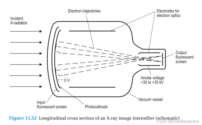
x射线图像增强器的纵向横截面(示意图)
While every effectively absorbed X-ray quantum in the X-ray screen generates several thousand light quanta, only a small fraction of these reach the photocathode, and thereby lead to the emission of photoelectrons representing a quantum yield of a few percent. One obtains a total of around 300 photoelectrons per absorbed X-ray quantum.
在x射线屏幕上,每一个有效吸收的x射线量子都能产生几千个光量子,但只有一小部分能到达光电阴极,从而导致光电子的发射,其量子产率只有几个百分点。每个被吸收的x射线量子总共获得大约300个光电子。
The electrons that are emitted in various directions from a point in the photocathode are deflected by the electric field in the interior of the image intensifier in such a way that their combined trajectories form a lobar bundle that attains its greatest thickness near the photocathode and becomes progressively narrower towards the anode. The electron trajectories converge again at a point (the image point) on the output fluorescent screen. The electrons take on kinetic energy as they move in the externally applied electric field. After traversing a potential difference of around 30 to 35 kV, the energy of an electron is sufficient to generate roughly one thousand light quanta in the output screen.
在各个方向发出的电子从一个点在光电阴极电场偏转的图像增强器的内部以这样一种方式,他们的轨迹相结合形成一个肺叶的包,达到它的最大厚度附近向阳极光电阴极,变得越来越窄。电子轨迹再次会聚在输出荧光屏上的一点(像点)。当电子在外部施加的电场中移动时,它们具有动能。在穿过大约30到35千伏的电位差后,一个电子的能量足以在输出屏幕上产生大约1000个光量子。
The information in an X-ray I.I. image is thus passed through several conversion stages:
x射线i . i图像中的信息因此经过几个转换阶段:

1吸收x射线量子 → 3000光量子
1吸收x射线量子 → 300年电子
1吸收x射线量子 → 300×1000光量子
The electric field in the X-ray I.I. has an effect on the photoelectrons that is similar to that of a focusing lens on light rays: an inverted (in this case substantially reduced) image arises. Given that all of the photo electrons emitted into the half-space are caught by the electron lens, electron-optical imaging qualifies as very efficient. The high luminance at the output fluorescent screen is achieved via the acceleration of the photoelectrons and via the concentration of the electron flux from the large photocathode area on the very much smaller output screen area. While the total luminous flux is not increased as a result of this second effect, the luminance is. The small, bright output image is very well suited for transmission to connected systems (e.g. CCD camera and imaging system with memory and monitor).
x射线I.I.中的电场对光电子的影响类似于聚焦透镜对光线的影响:产生一个倒转的(在这种情况下大大减少)图像。考虑到所有发射到半空间的光电子都被电子透镜捕获,电子光学成像可以被认为是非常有效的。输出荧光屏的高亮度是通过光电子的加速和从大的光电阴极区域到非常小的输出屏幕区域的电子通量的集中来实现的。虽然总光通量不会因为第二种效应而增加,但亮度却增加了。小而明亮的输出图像非常适合传输到连接的系统(如CCD相机和带有内存和监视器的成像系统)。
X-ray fluorescent screens (input screens) x射线荧光屏(输入屏)
The properties of the input phosphor have a major impact on the quality of the image transmission enabled by the X-ray image intensifier as a whole. The input phosphor determines the extent to which the X-ray quantum flux, which has to be kept as small as possible for reasons of radiation protection, can be exploited for image generation. Here, it is clearly necessary to find a compromise between the conflicting requirements of greater quanta absorption (large X-ray fluorescent layer thickness) and high resolution, which is diminished by excessively thick fluorescent layers due to the scattering of the generated light.
输入荧光粉的特性对x射线图像增强器的图像传输质量有很大的影响。输入的荧光粉决定了x射线量子通量的大小,由于辐射防护的原因,x射线量子通量必须尽可能地保持在较小的范围内,以便利用它来生成图像。在这里,显然有必要在更大的量子吸收(大x射线荧光层厚度)和高分辨率的相互矛盾的要求之间找到一个折衷方案,由于产生的光的散射,过厚的荧光层降低了高分辨率。
A breakthrough was made in this context as the X-ray fluorescent material zinc cadmium sulfide (ZnCdS: Ag) was replaced by cesium iodide (CsI:Na), an X-ray fluorescent material that combines several desirable properties in an almost ideal manner:
x射线荧光材料硫化锌镉(ZnCdS: Ag)被碘化铯(CsI:Na)取代,这是一个突破性的进展。碘化铯是一种x射线荧光材料,以近乎理想的方式结合了几个理想的性能:
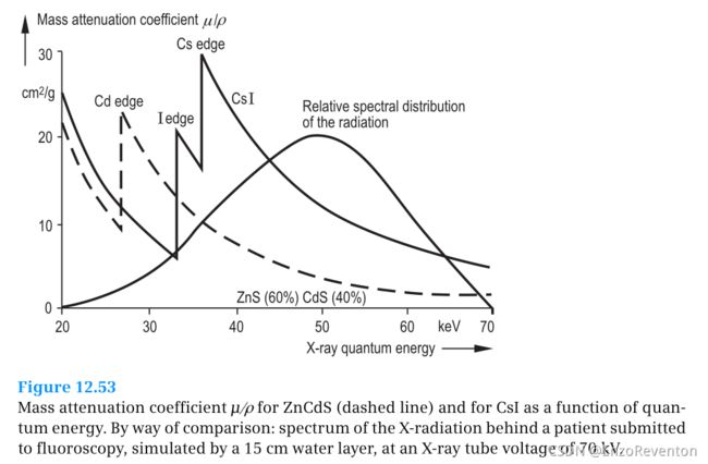 对于ZnCdS(虚线)和CsI,质量衰减系数μ/ρ作为量子能量的函数。比较:在x射线管电压为70千伏的情况下,用15厘米水层模拟接受透视的患者身后的x射线光谱。
- Favorable absorption values for X-ray quantum energies above the K-absorption edges of Cs (36 keV) and I (33 keV) (fig. 12.53) Cs (36 keV)和I (33 keV)的k吸收边以上x射线量子能的有利吸收值(图12.53)
- Good spectral matching to SbCs3 photocathodes (fig. 12.54), chemical compatibility with this photocathode 与SbCs3光电阴极具有良好的光谱匹配性(图12.54),与该光电阴极具有化学相容性
- Good vacuum properties (capacity to withstand degassing temperature) 良好的真空性能(耐脱气温度)
- Screen manufacture by vapor deposition 用气相沉积法制造筛网
- Packing density almost equal to that of the bulk material (in contrast to sedimentation screens exhibiting substantially lower packing densities) 堆积密度几乎与散装物料相当(与沉淀法筛相比,沉淀筛的堆积密度要低得多)
- Good adhesion of the vapor-deposited screen to aluminum sheet, enabling the easy production of any screen shape and narrow tolerances (important for the electron optics) 气相沉积屏幕与铝板的良好附着力,使任何屏幕形状和窄公差的生产变得容易(对电子光学很重要)
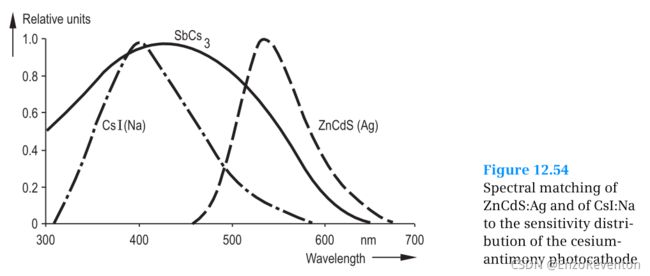
ZnCdS:Ag和CsI:Na与铯锑光电阴极灵敏度分布的光谱匹配

用扫描电子显微镜拍摄的Csl x射线屏幕破裂边缘的照片。顶部:x光屏的表面。中间:CsI晶体的破碎边缘(高度约450 μm)。底部:铝基板
If the vapor deposition process is carried out in a suitable manner, the screen will consist of continuous crystallites partially separated by fissures that are perpendicular to the substrate and that help to conduct the light in the desired direction (fig. 12.55). This enables one to significantly increase the thickness of the layer and hence the quantum absorption without sacrificing spatial resolution. The optimization of manufacturing processes allows one to produce needle-shaped crystallites with diameters of less than 10 μm [12.41], and thereby achieve an improvement in MTF.
如果以合适的方式进行气相沉积过程,屏幕将由连续的微晶组成,部分微晶被垂直于衬底的裂缝所分隔,这些裂缝有助于将光引导到所需的方向(图12.55)。这使得我们能够在不牺牲空间分辨率的情况下显著增加层的厚度和量子吸收。通过对制造工艺的优化,可以生产出直径小于10 μm的针状微晶[12.41],从而改善MTF。
12.3.2.3 Photocathode 光电阴极
The transparent photocathode in the X-ray image intensifier is made of antimony and one or more alkali metals (preferably cesium), which are deposited simultaneously or sequentially by vaporization in a thin layer (around 10 to 30 nm) [12.42]. The photocathode’s substrate is the X-ray screen (with or without a transparent intermediate layer). The spatial distribution of the photoelectron emission is thus a contact print of the instantaneous distribution of luminescent light in the X-ray screen.
x射线图像增强器中的透明光电阴极由锑和一种或多种碱金属(最好是铯)组成,它们同时沉积或依次蒸发在一薄层(约10至30 nm)中[12.42]。光电阴极的衬底是x射线屏(有或没有透明中间层)。因此,光电子发射的空间分布是x射线屏上荧光光瞬时分布的接触印版。
The service life of the photocathode – and thus of the X-ray image intensifier tube – extends to many years where conditions include constant room temperature and a good vacuum of around 10-6 mbar (it may be necessary to re-getter the vacuum). Longterm exposure to temperatures above approximately 35°C will have an adverse effect on the photocathode’s longevity.
如果条件包括恒定的室温和大约10-6毫巴的良好真空(可能需要重新获得真空),光电阴极和x射线图像增强管的使用寿命可以延长很多年。长期暴露在大约35°C以上的温度下将对光电阴极的寿命产生不利影响。
12.3.2.4 Electron optical imaging 电子光学成像
The photoelectrons that are emitted from each point of the photocathode and move off in all directions in the vacuum space are accelerated in the X-ray I.I.’s electron-optical system and focused as sharply as possible onto a corresponding point on the output screen. This is possible only to a limited extent, especially given the fact that the photoelectrons, apart from the direction of their distribution, also possess an initial energy of between 0 and approximately 1.3 eV. This is small in comparison to the acceleration voltage of 30 to 35 kV, but not negligible. Furthermore, it is also necessary to keep pincushion-shaped distortions small and the length of the X-ray I.I. tube short.
从光电阴极的每一点发射出来的光电子,在真空空间中向各个方向移动,在x射线i.i.s的电子光学系统中加速,并尽可能敏锐地聚焦到输出屏幕上的相应点上。这在一定程度上是可能的,特别是考虑到光电子除了其分布方向外,还具有0到大约1.3 eV的初始能量。与30至35千伏的加速电压相比,这是很小的,但不可忽略。此外,还需要保持针垫形状的扭曲较小和x射线I.I.管的长度较短。

数值计算具有两个聚焦电极的x射线图像增强器子午面的等势面和电子轨迹(初始光电子能:0.5 eV)
A planar output image is required for camera filming. A further requirement is the deployment of either a flat output screen or a fiber-optic plate with a hollow-ground inner surface coated with fluorescent material and a flat-ground outer surface.
相机拍摄需要平面输出图像。另一项要求是部署一个平面输出屏幕或一个光纤板,其内表面涂有荧光材料的空心地面,外表面是平面地面。
Electron optical imaging takes place via axial symmetric electrostatic potential distribution, which is produced by the photocathode, several auxiliary electrodes and the anode with the output screen. Favorable imaging properties will result if the photocathode has the shape of a rotation hyperboloid whose contour deviates only slightly from that of a spherical cap. This enables one to achieve a nearly flat output image. Fig. 12.56 shows a computer-generated potential distribution involving just a few electron trajectories.
光电成像是通过光电阴极、若干辅助电极和带有输出屏的阳极产生的轴对称静电势分布来实现的。如果光电阴极具有旋转双曲面的形状,其轮廓只稍稍偏离球帽的轮廓,就会产生良好的成像特性。这使人们能够获得几乎平坦的输出图像。图12.56显示了仅涉及几个电子轨迹的计算机生成的电位分布。
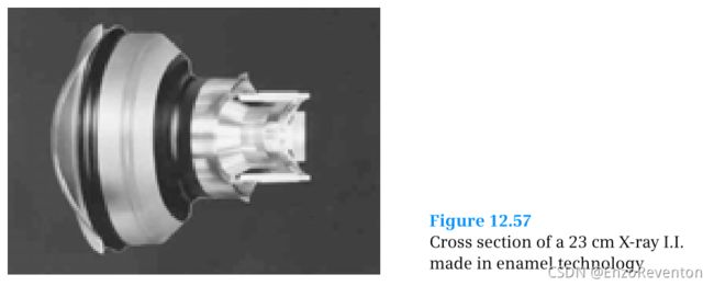
Deviations from the axially symmetric potential distribution lead to imaging errors (astigmatism). Electrode dimensional accuracy is therefore important. Fig. 12.57 shows the cross section of a 23 cm X-ray I.I. with the electrode system vapor deposited on enameled walls of stainless steel.
偏离轴对称电位分布导致成像误差(散光)。因此,电极尺寸精度很重要。图12.57显示了23厘米x射线i . i的横截面,其中电极系统蒸汽沉积在不锈钢的搪瓷壁上。
Electron optical imaging is very sensitive to external electric and magnetic fields. X-ray I.I. devices are therefore surrounded by a protective housing that is made of highly permeable sheet metal and sealed as well as possible. While this effectively screens out the geomagnetic field, it is necessary to avoid exposure to electric coils, magnets and power lines.
电子光学成像对外界电场和磁场非常敏感。因此,x射线i . i设备被一个由高渗透性金属板制成的保护外壳包围,并尽可能密封。虽然这有效地屏蔽了地磁场,但有必要避免暴露在线圈、磁铁和电线。
Large format modern X-ray image intensifiers typically offer electron-optical format switching (zoom). Keeping the anode voltage constant and changing only the focusing voltages enables one to map a (concentric) part of the input field onto the output screen, i.e. the electron-optical diminution is lessened and the image resolution increased while the image brightness is also reduced.
大画幅现代x射线图像增强器通常提供电子光学格式切换(缩放)。保持阳极电压不变,只改变聚焦电压,就可以将输入场的(同心)部分映射到输出屏幕上,即电子光学衰减减小,图像分辨率提高,同时图像亮度也降低。
12.3.2.5 Output screens 输出屏幕
X-ray image intensifier output phosphors consist of a uniform fluorescent layer (generally ZnCdS:Ag) that is a few micrometers thick and that is applied to a glass base that can simultaneously serve as the vacuum envelope’s image output window. The introduction of the finer and faster phosphor GdOS has led to an improvement in image quality. The feedback of light to the photocathode is prevented by covering the surface of the fluorescent layer with an aluminum skin that is opaque to light, but transparent to the high-energy electrons. The aluminum skin also serves as an equipotential surface and electrical connection to the anode.
x射线图像增强器输出荧光粉由一层均匀的荧光层(通常是ZnCdS:Ag)组成,这层荧光层有几微米厚,应用在玻璃基底上,同时作为真空包膜的图像输出窗口。更精细、更快的荧光粉GdOS的引入提高了图像质量。通过在荧光层的表面覆盖一层铝膜来阻止光线反馈到光电阴极,铝膜对光线不透明,但对高能电子透明。铝表皮也作为等电位面和与阳极的电连接。
Multiple reflections in the output screen’s glass base cause stray light and diminished image contrast. Contrast can be improved using tinted glass for the screen base. Useful light that passes only once through the base is attenuated less than stray light, which goes through the glass base at least three times. The use of a fiber-optic disk for the output screen’s base represents an effective, but expensive measure to bring about the selective attenuation of stray light.
输出屏幕玻璃底座的多次反射导致杂光和图像对比度降低。用有色玻璃做屏幕底座可以提高对比度。仅通过一次的有用光衰减小于杂散光,杂散光至少通过玻璃基座三次。使用光纤盘作为输出屏的基座是一种有效但昂贵的方法来实现杂散光的选择性衰减。
The best technical concept for stray light reduction involves making the output screen’s glass base roughly as thick as its radius. The totally reflected part of the stray light, which is the largest part, is then not directed back towards the fluorescent layer, but to the blackened edge of the screen base, where it is absorbed (fig. 12.58).
减少杂散光最好的技术概念是使输出屏幕的玻璃底座大致与其半径一样厚。杂散光的完全反射部分,也就是最大的部分,并没有被定向回荧光层,而是被屏幕基底的黑色边缘吸收(图12.58)。
12.3.2.6 Total gain factor, conversion factor 总增益因子、转换因子
As mentioned above, one obtains around 100 light quanta at the output screen for every light quantum emitted by the input screen into the photocathode. This factor is referred to as the lumen gain, although the term is slightly dubious because of the different luminescence spectra involved. The luminance ( c d / m 2 cd/m^2 cd/m2) is increased additionally by the ratio of the areas of the input and output screens (i.e. 50 to 200 for a typical X-ray II). The total luminance gain is thus around 1 0 4 10^4 104.
如上所述,对于输入屏发射到光电阴极的每一个光量子,在输出屏获得大约100个光量子。这个因素被称为流明增益,尽管这个术语有点可疑,因为涉及不同的发光光谱。亮度( c d / m 2 cd/m^2 cd/m2)还随着输入和输出屏幕面积的比例(即典型x射线II的50比200)而增加,因此总亮度增益约为 1 0 4 10^4 104。
It has become more common, however, to specify the conversion factor GX (cd/m2/μGy/s), which is the luminance at the output phosphor in relation to the dose rate of the incident radiation for standardized ICRU (International Commission on Radiological Units and Measurements) radiation quality, i.e. 20 mm Al-prefiltration and 7 mm first half-value aluminum thickness.
然而,规定转换系数GX (cd/m2/μGy/s)已变得更加普遍,这是标准ICRU(国际放射单位和测量委员会)辐射质量中输出荧光粉的亮度与入射辐射剂量率的关系,即20毫米铝预过滤和7毫米前半值铝厚度。
12.3.2.7 Resolving power, modulation transfer function (MTF), contrast ratio 分辨率、调制传递函数(MTF)、对比度
The resolving power (characterized by the MTF) of an X-ray image intensifier is determined by the two screens and the quality of the electron-optical imaging – in particular, the electron-optical diminution ratio. The resolving power can thus be increased by electron-optical zooming (fig. 12.59).
x射线图像增强器的分辨率(以MTF为特征)取决于两个屏幕和电子光学成像的质量,特别是电子光学衰减比。因此,通过电子光学变焦可以提高分辨率(图12.59)。
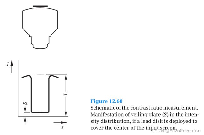
In addition to its spatial resolution, an X-ray I.I. is also characterized by its contrast resolution at low spatial frequencies, which can be measured by imaging a disc of lead (fig. 12.60). It turns out that the disk’s image brightness does not vanish altogether, even though it is entirely opaque to X-rays. The background brightness is referred to as veiling glare and is caused by the stray effects of X-ray quanta, photons and electrons in the X-ray I.I. tube.
除了空间分辨率外,x射线I.I.还具有低空间频率下的对比度分辨率,这可以通过成像铅盘来测量(图12.60)。事实证明,尽管x射线完全不透明,但圆盘的成像亮度并没有完全消失。背景亮度被称为遮蔽眩光,是由x射线I.I.管中x射线量子、光子和电子的杂散效应引起的。
A large amount of veiling glare leads to blurry images. This glare is characterized by the contrast ratio, i.e. the background brightness under an opaque disc related to the full brightness. Modern X-ray IIs have a contrast ratio of 35:1, measured using a lead disc that covers 10% of the input screen according to the IEC standard [12.43].
大量的遮蔽眩光导致图像模糊。这种眩光的特征是对比度,即不透明光盘下的背景亮度与全亮度相关。现代x射线的对比度为35:1,根据IEC标准[12.43],使用覆盖输入屏幕10%的引线盘测量。
12.3.3 Processing the X-ray image intensifier’s output image x射线图像增强器输出图像的处理
12.3.3.1 Second quantum sink 第二量子汇
The image intensifier (I.I.) provides a demagnified visible picture of the invisible X-ray image in real time. The size of this picture is too small to permit recognition of anatomic details with the naked eye and the picture’s brightness is not sufficient for optical magnification. The I.I.’s output screen is therefore recorded using a television (TV) camera and displayed as a large, bright and contrast-rich image on a TV screen. Furthermore, the fact that the electric signal of an electronic sensor can be digitized means that one can easily store, process and transmit the X-ray images.
图像增强器(I.I.)实时提供不可见x射线图像的非放大可见图像。这张照片的尺寸太小,肉眼无法识别解剖细节,照片的亮度也不足以进行光学放大。因此,人工智能的输出屏幕被电视摄像机记录下来,并在电视屏幕上显示为一个大的、明亮的、对比度丰富的图像。此外,电子传感器的电信号可以数字化,这意味着人们可以轻松地存储、处理和传输x射线图像。
The electrons generated by the impinging light in an electronic image sensor are the products of a multistage quantum process. This process is illustrated in fig. 12.61. The average total number of electrons generated in a pixel can be expressed by :
在电子图像传感器中,由碰撞光产生的电子是多级量子过程的产物。这个过程如图12.61所示。在一个像素中产生的电子的平均总数可以表示为:

a : 输 入 屏 的 平 均 吸 收 系 数 a:输入屏的平均吸收系数 a:输入屏的平均吸收系数
N : 撞 击 i . i 输 入 屏 幕 的 x 射 线 量 子 数 N:撞击i.i输入屏幕的x射线量子数 N:撞击i.i输入屏幕的x射线量子数
g i : 在 转 换 步 骤 i ( i = 1 , 2 , 3 , … ) 中 生 成 次 级 量 子 的 平 均 增 益 因 子 g_i:在转换步骤i (i = 1,2,3,…)中生成次级量子的平均增益因子 gi:在转换步骤i(i=1,2,3,…)中生成次级量子的平均增益因子
The fluctuations in the number of quanta in the pixel can be expressed by:
像素中量子数的波动可以表示为:
with average gain fluctuation at stage i:
在第一阶段有平均增益波动i:

第i阶段增益的方差
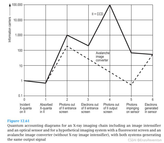
包括图像增强器和光学传感器的x射线成像链,以及带有荧光屏和雪崩图像转换器(没有x射线图像增强器)的假设成像系统的量子计算图,这两个系统产生相同的输出信号
Hence, the total fluctuation of the electrons in the electronic sensor (also referred to as photon shot noise) can be expressed as:
因此,电子传感器中电子的总涨落(也称为光子脉冲噪声)可以表示为:

and the detective quantum efficiency (DQE) (at spatial frequency u = 0) can be expressed as [12.44]
空间频率u = 0处的探测量子效率(DQE)可表示为[12.44]

(Here, it would be necessary to replace g i g_i gi with the product g i M T F i ( u ) 2 g_iMTF_i(u)^2 giMTFi(u)2 to obtain the spatial frequency dependence of the MTF.) The denominator in eq. (12.27) has to be close to 1 in order not to degrade the DQE. The signal-to-noise ratio in a multistage conversion process is determined by the lowest number of quanta. As shown in fig. 12.61, if an optical sensor is coupled to the X-ray I.I., the number of subsequent quanta (following the conversion of one X-ray quantum) is always high enough to avoid degrading the information generated by the impinging quantum flux. However, if one were to use an avalanche image converter with an X-ray fluorescent screen, the DQE would decrease as a result of the insufficient number of photons reaching the light sensitive area, although the output signal has the same signal amplitude. An effect referred to as the second quantum sink (the first being the absorption of the X-ray quanta in the fluorescent screen) thus occurs in the absence of an I.I.
(在这里,需要用产品 g i M T F i ( u ) 2 g_iMTF_i(u)^2 giMTFi(u)2替换 g i g_i gi,以获得MTF的空间频率依赖性。)为了不降低DQE, eq.(12.27)中的分母必须接近1。多级转换过程中的信噪比由最小的量子数决定。如图12.61所示,如果光学传感器耦合到x射线I.I.,则后续的量子数(在一个x射线量子转换后)总是足够高,以避免由碰撞量子通量产生的信息退化。然而,如果使用带有x射线荧光屏的雪崩图像转换器,DQE将会由于到达光敏区域的光子数量不足而减少,尽管输出信号具有相同的信号幅度。因此,在没有I.I.的情况下,就会出现被称为第二量子汇的效应(第一个是荧光屏对x射线量子的吸收)
12.3.3.2 Lens systems 透镜系统
A lens system is used to match the size of the I.I.’s output to that of the optical sensor’s input area. The relay optics for the X-ray I.I. are required to exhibit a large aperture and high optical transmittance in order to minimize the loss of photons. Image details are to remain free of blurring and distortion. Given that image sensors can only store a certain amount of electrons in their charge-integrating capacitors, it will be necessary to furnish the relay optics with a light control system. This enables one to reduce excess light (e.g. generated at high X-ray doses) before the occurrence of signal amplitude saturation. A combination of a motor driven iris and light absorbing filters in the light path is used for this purpose. The latter helps one to avoid excessively narrow iris openings in the case of bright objects that could cause disturbing optical effects (e.g. diffraction patterns or foreign-particle shadows in the image). Closing the iris will essentially reduce the DQE, however, doing so will have virtually no visual effect on the images.
一个透镜系统被用来匹配i.i.的输出和光学传感器的输入区域的大小。为了减少光子的损失,x射线I.I.的中继光学要求具有大口径和高光学透过率。图像细节保持不模糊和失真。由于图像传感器只能在电荷积分电容器中存储一定数量的电子,因此有必要为继电光学配备一个光控系统。这使人们能够在信号振幅饱和之前减少多余的光(例如在高x射线剂量下产生的光)。电机驱动的虹膜和光路中吸收滤光片的组合用于此目的。后者有助于避免在明亮物体的情况下过于狭窄的虹膜开口,这可能会导致干扰光学效应(如衍射图案或图像中的外来粒子阴影)。关闭虹膜将本质上减少DQE,然而,这样做将几乎没有视觉效果的图像。
The largest possible solid angle for light collection from the I.I. is provided by tandem optics (fig. 12.62). A telecentric beam configuration is usually applied with each of two individual lens systems focused to infinity. The magnifying ratio necessary to adapt the size of the I.I.’s output screen to the size of the sensor’s light-sensitive area can be expressed by the ratio of the focal length of the two lenses. A mirror or prism can be placed between the lenses to provide an additional light channel for exposure control. The output lens with the charge-coupled device (CCD) may be rotated to provide upright images at all angulations.
串联光学提供了从I.I.收集光的最大立体角(图12.62)。远心光束配置通常应用于两个独立透镜系统中的每一个,聚焦到无穷大。为了使i.i.的输出屏幕尺寸与传感器的光敏区尺寸相适应,所需的放大比可以用两个镜头的焦距比来表示。一个镜子或棱镜可以放置在镜片之间,以提供额外的光通道,以进行曝光控制。带有电荷耦合装置(CCD)的输出透镜可以旋转以提供所有角度的垂直图像。

i . i . ccd组合的双远心光学装置,光圈控制和曝光控制通道
12.3.3.3 Charge-coupled device (CCD) image sensors 电荷耦合器件(CCD)图像传感器
The image pick-up tubes that used to be deployed as optical sensors with image intensifiers (e.g. the Vidicon) have been replaced by high resolution, charge-coupled devices (CCDs) that satisfy virtually all diagnostic imaging requirements, including digital spot filming and motion studies. Fig. 12.63 shows a typical example of such a camera system.
图像采集管曾经作为带有图像增强器的光学传感器(如Vidicon)部署,现在已经被高分辨率、电荷耦合设备(ccd)所取代,这些设备几乎可以满足所有诊断成像需求,包括数字斑点拍摄和运动研究。图12.63显示了这种摄像系统的一个典型示例。
While the initial phases of their development date back to 1969, it was not until the late 1990s that charge-coupled devices (CCDs) had evolved to the point of meeting the relevant specifications (matrix size, signal-to-noise ratio) at production costs enabling their standard deployment as image sensors in X-ray TV chains. These devices are free of the typical disadvantages associated with image pick-up tubes, including temporal cathode degradation, dependence on several stabilized high supply voltages, high power consumption and large size.
在初始阶段的发展可以追溯到1969年,直到1990年代末,电荷耦合器件(ccd)进化的会议相关规范(矩阵大小、信噪比)的生产成本,使其标准部署在x射线图像传感器电视链。这些器件没有与图像采集管相关的典型缺点,包括时间阴极降解,依赖于几个稳定的高电源电压,高功耗和大尺寸。
Electron-hole pairs are generated in the depletion barrier of a silicon crystal when light photons impinge on the CCD’s photo sensitive area. The raising of the electrons from the valence band to the conduction band leaves holes in the valence band. Both charges are separated by an applied electric field. The charges can be displaced from one location to another if one moves their potential well by changing the potential distribution with an array of electrodes. The charges trapped under a single pixel are shifted serially to an output capacitor that feeds a signal processing circuitry.
当光子撞击到CCD的感光区域时,在硅晶体的耗尽势垒中产生电子-空穴对。电子从价带上升到导带,在价带上留下了空穴。两个电荷被外加电场分开。如果用电极阵列改变电极的电位分布,电荷可以从一个位置转移到另一个位置。捕获在单个像素下的电荷被连续地转移到一个输出电容上,该电容为信号处理电路提供信号。
Fig. 12.64 offers an illustration of the basics of charge transport for a three phase CCD design. Three electrodes are placed above each pixel. In the first phase, only the left electrode over the pixel has a positive potential, causing all of that pixel’s electrons to gather under that electrode. In the second phase, the middle electrode is also connected to the positive voltage and the charges are distributed under both electrodes. During the third phase, the left electrode is switched to negative and the electrons gather under the pixel’s middle electrode. The charge has thus been moved by a distance of one electrode (a third of a pixel). Charge movement amounts to a space of one pixel when the described scheme is applied three times.
图12.64给出了三相CCD设计中电荷传输的基本原理。三个电极被放置在每个像素的上方。在第一阶段,只有像素上的左电极具有正电位,导致该像素上的所有电子聚集在该电极下。在第二相中,中间电极也与正电压相连,电荷分布在两个电极下方。在第三阶段,左电极转换为负极,电子聚集在像素的中间电极下。电荷因此被移动了一个电极的距离(1 / 3像素)。当所述方案应用三次时,电荷移动相当于一个像素空间。
Many charge carriers are integrated into the pixel capacitors before read out. The voltage across the pixel capacitor increases during charge accumulation. If the voltage exceeds a certain level (full well capacity), charges can spill over to adjacent pixels, an effect called blooming. To avoid this, CCDs for X-ray imaging need to be furnished with an anti-blooming mechanism. A drain electrode is located in the substrate under each pixel. To protect against overload, the substrate voltage can be set to a potential that will trigger the draining of surplus charges into the substrate during the CCD’s inte-
gration period.
在读出之前,许多载流子被集成到像素电容器中。在电荷积累过程中,像素电容器上的电压增加。如果电压超过一定的水平(满井容量),电荷就会溢出到邻近的像素上,这种效果叫做“晕屏”。为了避免这种情况,用于x射线成像的ccd需要配备防晕装置。漏极位于衬底的每个像素下方。为了防止过载,可以将衬底电压设置为一个电位,该电位将触发CCD集成期间剩余电荷向衬底排放。
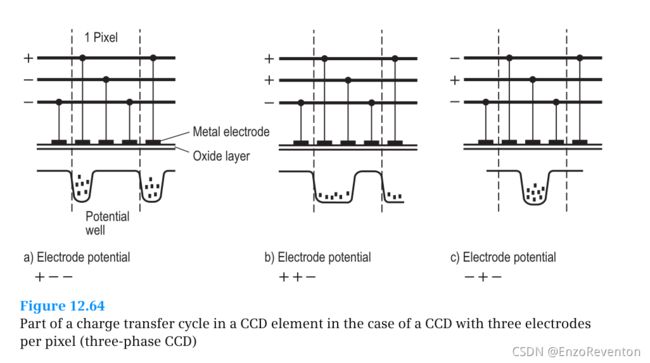
在每像素有三个电极的CCD(三相CCD)的情况下,CCD元件中的电荷转移循环的一部分
12.3.3.4 CCD architecture CCD架构
CCDs come in various architectures [12.45]. The simplest is the full frame (FF) CCD (fig. 12.65). Here, the integrated charges are shifted line by line into a horizontal readout register after image acquisition. The FF-CCD is ready for a new image only after all the charges have been read out because smearing effects occur when light impinges on the photosensitive array during the charge transport. The frame transfer (FT) concept allows for a higher frame rate. The FT-CCD is divided into three areas: the image area, the storage area and the horizontal read-out register (fig. 12.66). The read-out register is shielded against light by an aluminum cover. Image signals can be read out while a new image frame is acquired as soon as the integrated charges have been moved to the storage area.
ccd有不同的架构[12.45]。最简单的是全帧(FF) CCD(图12.65)。在这里,集成电荷在图像采集后逐行移位到水平读出寄存器中。因为在电荷传输过程中,当光撞击到光敏阵列上时,会产生涂抹效应,所以只有在读出所有电荷后,FF-CCD才会产生新的图像。帧传输(FT)的概念允许更高的帧率。FT-CCD被分为三个区域:图像区、存储区和水平读出寄存器(图12.66)。读出寄存器用铝盖遮光。一旦集成电荷被转移到存储区域,图像信号就可以读取,同时获取新的图像帧。
The interline transfer (IT) CCD design (fig. 12.67) enables one to avoid smearing effects to a very high degree thanks to the fact that no charge transport takes place across a photosensitive area. The charges of each photo site are transferred virtually instantaneously (i.e. within a few nanoseconds) into light-shielded vertical shift registers that then transfer the charges into the horizontal output register. However, as in the case of IT-CCDs of the same size, the light sensitive area is smaller than that of FF and FT-CCDs (i.e. they are less sensitive).
线间传输(IT) CCD设计(图12.67)使人们能够在很大程度上避免涂抹效应,因为在光敏区不发生电荷传输。每个照片位置的电荷几乎在瞬间(即在几纳秒内)转移到光屏蔽的垂直移位寄存器,然后转移到水平输出寄存器。但是,在相同尺寸的it - ccd的情况下,光敏面积比FF和ft - ccd小(即灵敏度较低)。
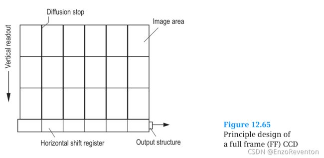
全帧(FF) CCD的原理设计

帧传递(FT) CCD的原理设计

线间传输(IT) CCD的原理设计
12.3.3.5 CCD noise sources CCD噪声源
When considering CCD noise it is important to draw a distinction between stochastic and systematic noise [12.46]. The composition of stochastically fluctuating noise charges can be expressed as:
考虑CCD噪声时,区分随机噪声和系统噪声是很重要的[12.46]。随机波动噪声电荷的组成可以表示为:

Dark noise N D a r k = q T h e r m a l N_{Dark} = \sqrt{q_{Thermal}} NDark=qThermal stems from thermally generated electrons q T h e r m a l q_{Thermal} qThermal in the light sensitive and storage areas. The value of qThermal q T h e r m a l q_{Thermal} qThermal increases exponentially along with temperature.
暗噪声 N D a r k = q T h e r m a l N_{Dark} = \sqrt{q_{Thermal}} NDark=qThermal来自于光敏区和存储区的热生电子 q T h e r m a l q_{Thermal} qThermal。 q T h e r m a l q_{Thermal} qThermal的值随温度呈指数增长。
Transfer-inefficient shot noise N T r a n s f e r N_{Transfer} NTransfer results from the stochastically fluctuating loss of electrons during charge transfer from the light sensitive area to the read-out capacitor. This noise is generated by a multistage process that is similar to that described by eq. (12.23) and depends on signal intensity.
转移效率低的散粒噪声 N T r a n s f e r N_{Transfer} NTransfer是由于电荷从光敏区转移到读出电容时电子的随机波动损失造成的。这个噪声是由一个类似于eq.(12.23)所描述的多阶段过程产生的,并且取决于信号强度。
Photon shot noise N S h o t N_{Shot} NShot has already been explained (section 12.3.3.1). As has been shown, the number of electrons generated per optical photon in the CCD will have to be as high as possible and the CCD will have to be furnished with sufficient full well capacity.
光子散粒噪声 N S h o t N_{Shot} NShot已经解释过了(章节12.3.3.1)。如前所述,在CCD中每个光子产生的电子数量必须尽可能高,并且CCD必须具有足够的充分容量。
Reset noise N R e s e t = k T C N_{Reset} = \sqrt{kTC} NReset=kTC (T: Temperature) is thermal noise generated by the channel resistance of the field effect transistor (FET) that resets the sense capacitor C. Reset noise can be avoided via correlated double sampling, a procedure that measures the difference between reset and signal level.
复位噪声 N R e s e t = k T C N_{Reset} = \sqrt{kTC} NReset=kTC(T:温度)是由场效应晶体管(FET)的通道电阻产生的热噪声,它对感知电容c进行复位。复位噪声可以通过相关的二次采样来避免,这是一种测量复位和信号电平之间差异的方法。
Output amplifier noise N A m p ∝ Δ f N_{Amp} ∝ \sqrt{Δf} NAmp∝Δf arises from the analog signal processing circuits (1/frequency and resistive noise). It depends on temperature and on the bandwidth Δf, which is inversely proportional to the read-out time.
输出放大器噪声 N A m p ∝ Δ f N_{Amp} ∝ \sqrt{Δf} NAmp∝Δf来自模拟信号处理电路(1/频率和电阻噪声)。它取决于温度和带宽Δf,带宽与读出时间成反比。
Dark noise in CCDs for X-ray imaging is very small, down to 5 equivalent electrons. The noise generated by all other noise sources can be as large as 75.
用于x射线成像的ccd中的暗噪声非常小,低至5个等效电子。所有其他噪声源产生的噪声可高达75。
Regular disturbance structures extending across a uniformly illuminated CCD image are referred to as fixed pattern noise (FPN). These structures originate from small deviations in the CCD manufacturing process (e.g. nanometer-range errors in the alignment of the various photomasks deployed). These non-uniformities are usually so small that they do not hinder diagnostic procedures. Given higher requirements, however, image homogeneity can be augmented via flatfielding. Flatfielding involves acquiring and storing a zero image and then subtracting this zero image from the actual image during the image acquisition phase.
在均匀照明的CCD图像上延伸的规则扰动结构称为固定模式噪声(FPN)。这些结构源于CCD制造过程中的小偏差(例如,不同掩模排列时的纳米范围误差)。这些不均匀性通常很小,并不妨碍诊断过程。然而,在更高的要求下,可以通过平场增强图像的均匀性。平场包括获取和存储一个零图像,然后在图像采集阶段从实际图像中减去这个零图像。
The same principle can also be applied to level out the small pixel sensitivity variations. Each pixel’s actual signal will then have to be multiplied by its stored zero-image value to obtain homogeneous signal distribution at all illumination levels.
同样的原理也可以用于消除微小的像素灵敏度变化。每个像素的实际信号将必须乘以其存储的零图像值,以获得均匀的信号分布在所有光照水平。
12.3.3.6 Other CCD properties CCD的其他属性
In contrast to some types of pick-up tubes, the amplitude response of a CCD is strictly linear. A deviation from signal linearity is to be expected only in the case of very high signals near the CCD’s saturation point (where the anti-blooming mechanism begins to work).
与某些类型的拾取管相比,CCD的幅值响应是严格线性的。只有在靠近CCD饱和点(即防晕机制开始工作的地方)的高信号情况下,信号线性度才会发生偏差。
Given that they involve a different scanning principle, CCDs offer a further advantage of being free of the ghost images that sometimes appear in connection with pick-up tubes. Therefore, CCDs do not limit overall temporal resolution when coupled with an X-ray I.I.
由于它们涉及到不同的扫描原理,ccds 提供了一个进一步的优势,即不会出现有时与拾取管有关的鬼影图像。因此,当使用 x 射线 i.i. 时,ccds 并不限制总时间解析度。
The imperfections in the scanning electron optics (as well as in the image itself) that are associated with pick-up tubes can degrade performance. In contrast to pick-up tubes, the MTF of a CCD is perfectly uniform across the sensor area. A CCD’s MTF (when indicated in line pairs per picture height) is superior to a tube’s MTF when operated at the same scanning matrix.
扫描电子光学(以及图像本身)的缺陷与拾取管可以降低性能。与拾取管相比,ccd 的 mtf 在整个传感器区域非常均匀。当在相同的扫描矩阵下工作时,ccd 的 mtf (当以每幅图像高度的线对表示时)优于管道的 mtf。
Given that virtually no charges are lost during transfer, the MTF of a CCD that is used in X-ray imaging is only dependent on the pixel aperture. A CCD thus enables the realization of an MTF at the theoretical limit established by the pixel size and the imaging matrix. However, if CCDs are deployed as digital detectors coupled to a scintillator layer (as is the case in mammography), the image quality in terms of MTF and DQE will largely depend on the scintillator and the optical coupling to the sensor.
考虑到传输过程中几乎不会丢失电荷,用于 x 射线成像的 ccd 的 mtf 仅依赖于像素孔径。因此,ccd 能够在由像素尺寸和成像矩阵确定的理论极限上实现 mtf。然而,如果将 ccd 作为耦合到闪烁体层的数字探测器部署(如同乳房 x 光摄影中的情况) ,则 mtf 和 dqe 的图像质量将在很大程度上取决于闪烁体和与传感器的光学耦合。
12.3.3.7 Video signal digitization 视频信号数字化
Given that digital signals provide more freedom with respect to image processing, storage and display, the CCD’s analog output signal is digitized using an analog-todigital converter (ADC) that is usually integrated into the camera (fig. 12.68). Output signal filtering is necessary prior to digitizing the CCD so as to cut off all frequencies above half the sampling frequency and thereby avoid aliasing and additional noise.
由于数字信号在图像处理、存储和显示方面提供了更大的自由度,ccd 的模拟输出信号通过通常集成到相机中的模数转换器(adc)进行数字化(图12.68)。在对 ccd 进行数字化之前,必须对输出信号进行滤波,以便切断采样频率一半以上的所有频率,从而避免混叠和附加噪声。

对模拟图像信号进行数字化
The ADC is usually a monolithic MOS circuit. The analog input signal is quantized into 2 N 2^N 2N (N is the resolution of the ADC in bits) equal amplitude intervals. Each quantization level is assigned to an integer between 0 and 2 N – 1 2^{N–1} 2N–1. This number is turned into binary code by the ADC, which represents it on N separate output lines (fig. 12.68). In principle, one has to accept a loss of information (least significant bit or LSB) according to ±1/2 of the quantization step (least significant bit or LSB).
Adc 通常是单片 mos 电路。将模拟输入信号量化为 2 N 2^N 2N (n 是 adc 的分辨率,以位为单位)等幅区间。每个量化水平被分配给0到 2 N – 1 2^{N–1} 2N–1之间的整数。这个数字被 adc 转换成二进制代码,在 n 个单独的输出线上表示它(图12.68)。原则上,必须根据量化步骤的 ± 1/2接受信息的丢失(最低有效位或 lsb)。
The number of necessary bits can be calculated by dividing the CCD’s full well (e.g. 170,000 electrons) for a single scan by the electronic noise floor (e.g. 75 electrons). Here, a 12 bit ADC would be required for a low noise CCD camera. However, 10 bit ADCs are also used with CCD cameras for X-ray imaging.
用电子噪声层(例如75个电子)除以 ccd 的全阱(例如170,000个电子)就可以计算出一次扫描所需的位数。在这里,低噪声 ccd 相机需要12位 adc。然而,10位 adc 也用于 ccd 摄像机的 x 射线成像。
12.3.3.8 CMOS sensors cmos 传感器
The proven technology deployed in the latest CCDs offers a fully satisfactory solution for X-ray TV cameras. CMOS image sensors may become an interesting alternative in the future. These promise higher scanning speeds, lower noise levels, advanced circuit miniaturization and greater energy efficiency. The principle behind a CMOS image sensor is shown in fig. 12.69. The light sensitive area can be read out in an arbitrary order. This enables one to track rapidly changing details in a reduced image area via a significantly faster readout.
新的 ccd 采用了成熟的技术,为 x 射线电视摄像机提供了完全令人满意的解决方案。Cmos 图像传感器将来可能会成为一种有趣的替代品。这些承诺更高的扫描速度,更低的噪音水平,先进的电路小型化和更高的能源效率。有源像素传感器的原理如图12.69所示。光敏区域可以按任意顺序读出。这使人们能够跟踪快速变化的细节,在缩小的图像区域,通过显着更快的读出。

X-y 可寻址有源像素传感器的设备架构
12.3.4 Flat detectors 平面探测器
The flat detector (FD) established itself as the prime standard in digital X-ray imaging in the late 1990s. Flat detectors designed for use in projection radiography and mammography continue to replace analog screen-film combinations and digital storagephosphor systems. In the areas of cardiac angiography and pediatric cardiac imaging, flat detectors offering real-time imaging of up to 30 frames per second (fps) or even 60 fps have become a popular replacement for the image intensifier. Similar changes are taking place in general angiography and in fluoroscopy. Flat detectors offer a tantalizing all-in-one potential: a single technology covering all diagnostic and interventional applications in X-ray imaging [12.47, 12.48].
平面探测器(fd)在20世纪90年代末成为数字 x 射线成像的主要标准。用于放射照相和乳房 x 光摄影的平板探测器继续取代模拟屏幕-胶片组合和数字存储荧光体系统。在心血管造影和儿童心脏成像领域,平板探测器提供高达30fps (fps)甚至60fps 的实时成像,已经成为图像增强器的普遍替代品。类似的变化也发生在全身血管造影和透视中。扁平探测器提供了一个诱人的多合一的潜力: 一个单一的技术,涵盖所有诊断和介入应用的 x 射线成像[12.47,12.48]。
In what follows, we introduce the subject of flat detector technology and its two basic designs: indirect conversion and direct conversion. After describing the required calibration and the steps involved in image processing, we present an overview of basic flat detector performance characteristics. We then turn to a discussion of the many advantages associated with flat detector technology and how these advantages relate to workflow and new applications. We conclude our discussion with a brief look at future developments.
接下来,我们介绍了平面探测器技术及其两种基本设计: 间接转换和直接转换。在描述了所需的校准和图像处理所涉及的步骤之后,我们提出了一个基本的平板探测器性能特点的概述。然后,我们将讨论扁平检测器技术的许多优点,以及这些优点与工作流和新应用程序的关系。我们以对未来发展的简短展望来结束我们的讨论。
12.3.4.1 Flat detector design and technology 平面探测器设计和技术
The purpose of any medical imaging X-ray detector is to efficiently absorb the impinging X-ray flux and to convert this flux into a geometry-conserving digital image signal. In general, one should keep the unavoidable additional electronic noise generated during the numerous conversion and amplification steps to a minimum while maintaining the levels of spatial and contrast resolution that are required for the respective applications. Detective quantum efficiency (DQE) has become the fundamental physical parameter. This parameter describes a detector’s ability to efficiently convert the X-ray radiation at its input into a useful image signal at its output. The objective of any developmental work in detector technology must be to either reach or surpass the established DQE levels. Besides DQE, the following design parameters are used to characterize detectors: a) dynamic range, b) maximum image acquisition rate, c) active area, d) pixel size, e) device size and f) weight. The values for all of these parameters need to be selected carefully so as to best match the detector’s intended application.
任何医学成像 x 射线探测器的目的都是有效地吸收撞击的 x 射线通量,并将其转换成几何保护的数字图像信号。一般而言,我们应尽量减少在多次转换及放大过程中不可避免产生的额外电子噪音,同时保持各项应用所需的空间及对比度分辨率。探测量子效率(dqe)已经成为基本的物理参数。这个参数描述了探测器有效地将输入的 x 射线辐射转换为输出的有用图像信号的能力。任何探测器技术开发工作的目标必须达到或超过既定的 dqe 水平。除了 dqe,以下设计参数被用来表征探测器: a)动态范围,b)最大图像采集率,c)有效面积,d)像素大小,e)设备大小和 f)重量。需要仔细选择所有这些参数的值,以便最好地匹配检测器的预期应用程序。
Flat detector technology is the only detector technology available today that covers the various requirements of the entire application spectrum, ranging from general radiography to mammography, angiography and fluoroscopy.
平板探测器技术是目前唯一可用的探测器技术,它涵盖了整个应用范围的各种要求,从普通 x 线摄影到乳房 x 线摄影、血管造影和透视。
Active readout matrices for flat detectors 平面探测器主动读出矩阵
The development of liquid crystal display (LCD) technology for the consumer market as a replacement for monitors based on cathode ray tubes has introduced a technology whose characteristics are also ideally suited to sensors in medical X-ray imaging. This technology is based on hydrogenated amorphous silicon (a-Si:H) that can be deposited in the form of a thin film. Amorphous silicon combines several favorable characteristics. First, it possesses the relevant semiconductor properties, including doping, photoconductivity and junction formation. This makes a-Si:H suitable for the manufacture of electrical components such as switching transistors (thin film transistors, TFT) and photodiodes, but not for amplification circuits. Second, the material permits large-format deposition and thus enables one to deploy large active matrices (exceeding 40×40 cm2) of several million pixels (fig. 12.70). These active matrices represent the central component of flat detectors. Third, amorphous silicon exhibits high radiation hardness, making it suitable for applications in medical X-ray imaging.
随着液晶显示器(lcd)技术在消费市场的发展,以取代基于阴极射线管的显示器,这项技术引进了一种特性也非常适合医用 x 射线成像传感器的技术。这种技术基于氢化非晶硅(a-si: h) ,可以以薄膜的形式沉积。非晶硅结合了几个有利的特点。首先,它具有相关的半导体特性,包括掺杂、内光电效应和结的形成。这使得 a-si: h 适用于制造诸如开关晶体管(薄膜晶体管,tft)和光电二极管等电子元件,但不适用于放大电路。第二,材料允许大幅面沉积,因此可以部署几百万像素的大型有源矩阵(超过40 × 40立方厘米)(图12.70)。这些有源矩阵代表了扁平探测器的中心组成部分。第三,非晶硅具有很高的辐射硬度,适用于医疗 x 射线成像。

A-si 有源矩阵传感器像素结构的显微图像,显示光电二极管、 tft、门、偏置和数据线
Two different processes for converting X-ray radiation into electric charge are used. The first process (indirect) involves first converting the X-ray radiation into light and then using the absorption of this light to generate electric charge. The second process involves directly converting X-ray quanta into electric charge.
使用两种不同的方法将 x 射线辐射转化为电荷。第一个过程(间接的)首先将 x 射线辐射转化为光,然后利用这种光的吸收产生电荷。第二个过程是直接把 x 射线量子转换成电荷。
Flat detectors based on an indirect conversion process 基于间接转换过程的平面探测器
The most widely used flat detector design today is based on a two-level, indirect conversion process (fig. 12.71). The photo absorption of the X-ray quantum generates a high energy electron. While losing energy in the scintillator material, the electron creates a large number of electron-hole pairs, which in turn recombine to produce photons in the visible range. This light subsequently strikes the photodiode where it is converted to electric charge. This two-step conversion process has the advantage of permitting one to optimize each step relatively independently of the other. Fig. 12.72 offers an illustration of such a detector.
目前使用最广泛的平面探测器设计是基于两级间接转换过程(图12.71)。X 射线量子的光吸收产生了一个高能电子。当闪烁体材料失去能量时,电子产生大量的电子-空穴对,这些电子-空穴对反过来重组产生可见范围内的光子。这种光随后击中光电二极管,在那里转化为电荷。这两个步骤的转换过程的优点是允许一个优化每一个步骤相对独立于其他。图12.72展示了这种探测器。

间接 x 射线转换过程
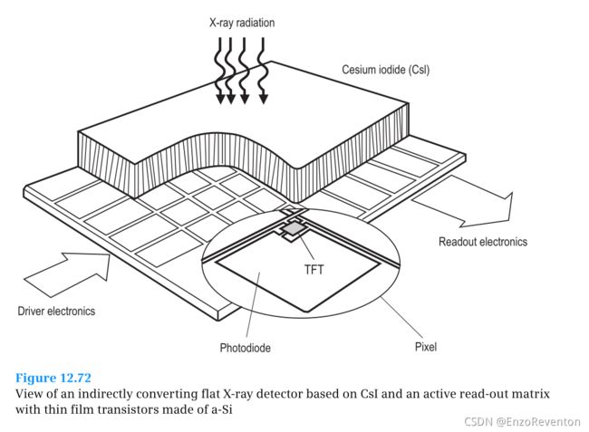
本发明提供了一种基于 csi 的间接转换平面 x 射线探测器和由 a-si 制成的薄膜晶体管的有源读出矩阵
Suitable scintillators for flat detectors include gadolinium oxysulfide ( G d 2 O 2 S Gd_2O_2S Gd2O2S) and thallium-doped cesium iodide (CsI:Tl) – CsI being the scintillator of choice. While CsI:Na is already well established in image intensifier technology, the alternative Tl doping substance used for flat detectors shifts the color of the fluorescent light from blue to green, thereby providing a better match for the spectral sensitivity of the photodiode. A thickness of about 500 μm yields absorption values of > 80% for a typical Xray spectrum at 70 kV. The a-Si photodiode is designed for a large geometric aperture covering 70% of the pixel area (geometric fill factor) at a pixel size of about 150 μm. Taking all effects into account, an absorbed X-ray quantum with an energy of 60 keV will generate about 1,000 electrons in the a-Si photodiode.
适用于平板探测器的闪烁晶体包括硫氧化钆(gd2o2s)和掺铊碘化铯(csi: tl)-csi 是首选的闪烁晶体。虽然 csi: na 在像增强技术方面已经很成熟,但用于平板探测器的替代 tl 掺杂物质将荧光灯的颜色从蓝色转换为绿色,从而为光电二极管的光谱敏感度提供了更好的匹配。厚度约为500微米产生的吸收值大于80% 的典型 x 射线光谱在70千伏。非晶硅光电二极管设计用于在像素大小约为150微米的情况下覆盖像素面积的70% (几何填充因子)的大几何孔径。考虑到所有的影响,一个能量为60千电子伏的吸收 x 射线量子,将在 a-si 光电二极管中产生大约1000个电子。
Fig. 12.73 shows the electric circuit of a TFT-based pixel structure. The photodiode, which acts as a capacitor, is charged to full-bias voltage prior to X-ray radiation while the TFT remains in the off state. The absorption of the incident light that is generated in the photodiode during X-ray radiation creates electron-hole pairs. These pairs drift to opposite contacts and gradually discharge the photodiode. The readout is initiated when the TFT is switched on via the gate line. This causes charge to flow to the photodiode, thus leading to the restoration of the data-line voltage. The charge flow is measured in the external electronics and recorded as the signal. Given that this step resets the photodiode to full bias, the pixel is ready for the next acquisition.
图12.73示出了基于 tft 的像素结构的电路。作为电容器的光电二极管,在 x 射线辐射之前充满全偏置电压,而 tft 保持关闭状态。在 x 射线辐射期间在光电二极管中产生的对入射光的吸收产生了电子-空穴对。这些对漂移到相反的接触,并逐渐放电的光电二极管。当 tft 通过门线打开时,读数就开始了。这导致电荷流向光电二极管,从而导致恢复数据线电压。电荷流在外部电子器件中测量并记录为信号。假设这一步将光电二极管重置为完全偏置,像素就可以进行下一次采集了。
The readout is performed row by row and addresses all pixels in a given row simultaneously. Optimized low-noise electronic circuits with high bandwidths are used to measure the charge and amplify the signal. Such application-specific integrated circuits (ASICs) may be connected to as many as 120 or more individual readout channels. The readout chip also functions as a multiplexer that feeds the signals to an ADC. At this stage the signal is available for further processing in the image processing chain.
读出是一行一行地执行的,并且同时地址给定行中的所有像素。采用优化的高带宽低噪声电路测量电荷,放大信号。这种应用专用集成电路(专用集成电路)可以连接多达120个或更多的单个读出通道。读出芯片还可以作为多路复用器,将信号输入 adc。在这个阶段,信号可用于图像处理链中的进一步处理。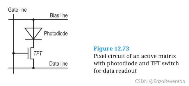
用于数据读出的带有光电二极管和 tft 开关的有源矩阵像素电路
Flat detectors based on a direct conversion process 基于直接转换过程的平面探测器
The direct detection process is depicted in fig. 12.74. The absorption of the X-ray in the photoconductor material generates a high energy electron. This electron loses its energy as it passes through the material, thereby creating many electron-hole pairs. An electric field applied across the detection material is used to collect the generated charge carriers.
直接检测过程如图12.74所示。光导体材料对 x 射线的吸收产生高能电子。这个电子在穿过材料时会失去能量,从而产生许多电子空穴对。施加在所述检测材料上的电场用于收集所述产生的电荷载流子。
The suitability of a material for use in direct converters is determined by the following basic characteristics: a) high X-ray absorption, b) generation of a large number of charge carriers for each absorbed X-ray, c) high charge-carrier collection efficiency and d) low dark current. The subjects of current research include photoconductor materials exhibiting high atomic numbers and densities and therefore good absorption characteristics (e.g. PbI, PbO, CdTe and HgI). However, the best understood and most frequently used material is amorphous selenium (a-Se). This material can be deposited directly onto an a-Si active matrix, with each pixel consisting of an electrode and a TFT, used for charge storage and charge readout, respectively.
直接转换器材料的适用性取决于以下基本特性: a)高的 x 射线吸收,b)每吸收一次 x 射线就产生大量的电荷载流子,c)高的电荷载流子收集效率和 d)低的暗电流。目前的研究对象包括具有高原子序数和高密度,因此具有良好吸收特性的光导体材料(如 PbI, PbO, CdTe,HgI)。然而,最好的理解和最常用的材料是无定形硒(硒)。这种材料可以直接沉积在 a-si 有源矩阵上,每个像素由一个电极和一个 tft 组成,分别用于存储电荷和读出电荷。
Due to its low-lying K-edge, a-Se is particularly well suited to the X-ray spectra used in mammography. A selenium thickness of 250 μm is adequate for mammography applications involving X-ray energy levels of around 30 keV. However, sufficient absorption can only be obtained in general radiography and fluoroscopy with a ‘thick’ a-Se layer of around 1 mm due to selenium’s relatively low atomic number (Z = 34). Depending on the energy of the absorbed X-ray, anywhere from several hundred to more than a thousand charge carriers are generated and then transported to the electrode of the respective pixel via the applied electric field. A portion of the generated charge is lost via recombination and deep trapping as the charge carriers pass through the material to the storage electrode. A voltage of approximately 10 kV or more is applied across a 1 mm selenium layer to obtain sufficient charge-collection efficiency. This in turn requires special care in pixel design in order to protect the TFT against damage.
由于它的 k 型边缘较低,a-se 特别适合 x 光摄影中使用的 x 光光谱。250微米的硒厚度足以用于乳腺 x 射线照相,x 射线能级约为30千电子伏。然而,由于硒的原子序数相对较低(z = 34) ,只有在普通 x 线摄影和荧光透视中才能获得足够的吸收,“厚”的 a-se 层大约为1毫米。根据被吸收的 x 射线的能量,产生几百到一千多个电荷载流子,然后通过外加电场传输到各自像素的电极。当所述电荷载流子通过所述材料到所述存储电极时,所述产生的电荷的一部分通过复合和深陷阱丢失。在一毫米硒层上施加大约10千伏或更高的电压,以获得足够的电荷收集效率。这反过来又需要在像素设计中特别注意,以保护 tft 免受损害。
Charge readout is accomplished by addressing the TFTs line by line, recharging the electrodes via the data line and measuring the respective signals in the peripheral low-noise readout electronics. The amplified signals are sequentially converted to digital signals via one or more ADCs. The signal is then fed to the image processing chain for further processing.
电荷读出是通过逐行寻址 tft 线,通过数据线给电极充电和测量外围低噪声读出电子学中各自的信号来完成的。放大的信号通过一个或多个 adc 顺序转换成数字信号。然后将信号反馈给图像处理链进行进一步处理。
12.3.4.2 Image pre-processing for flat detectors 平面探测器图像预处理
Further data processing is required before the image data generated by flat detectors can be displayed for medical purposes. This further processing includes a) image preprocessing, b) image post-processing and c) final image processing at the display medium. While the first step is specific to a given flat detector whose characteristics need to be matched, the remaining two steps apply in general to all digital X-ray detector technologies, such as computed radiography and image intensifier CCD-camera systems.
平板探测器产生的图像数据需要进行进一步的数据处理才能用于医学目的。该进一步处理包括 a)图像预处理,b)图像后处理和 c)显示介质上的最终图像处理。虽然第一步是针对特定的平板探测器,其特性需要匹配,其余两步通常适用于所有数字 x 射线探测器技术,如计算机放射成像和像增强器 ccd-camera 系统。
Image pre-processing for flat detectors is usually required to generate artifact-free images from the generated raw data. The most common types of artifacts stem from a) pixel-to-pixel sensitivity variations, b) pixel-to-pixel dark-current variations, c) horizontal and vertical structures arising from channel-to-channel driver and readoutcircuitry variations and d) inhomogeneous illumination of the radiation field.
平面探测器的图像预处理通常需要从生成的原始数据中生成无伪影的图像。最常见的伪影类型源于 a)像素-像素灵敏度变化 b)像素-像素暗电流变化 c)水平和垂直结构产生于通道-通道驱动器和读出电路变化 d)辐射场的不均匀照明。
Offset and gain corrections are carried out to remove such background patterns. Such flatfielding is applied for each individual pixel in the image matrix. The corrected image I i j ( t ) I_{ij}(t) Iij(t) is calculated on the basis of the raw image X i j ( t ) X_{ij}(t) Xij(t)acquired at time t for each pixel ij in row i and column j according to the formula where O i j ( t 1 ) O_{ij}(t1) Oij(t1) is the offset image taken at time t1 and where denotes the gain image derived at time t2 from a set of X-ray and offset images, XG and OG, respectively. Here, the raw image XG is generally acquired under conditions similar to those actually used in the application (with respect to X-ray spectrum, dose and geometry). Offset images, in contrast, are acquired without radiation.
进行偏移和增益校正以去除这些背景图案。对图像矩阵中的每个单独像素应用这种平面场地分析。校正图像 I i j ( t ) I_{ij}(t) Iij(t)是根据行 i 和列 j 中每个像素 ij 在时间 t 时获得的原始图像 X i j ( t ) X_{ij}(t) Xij(t)计算的,公式中 O i j ( t 1 ) O_{ij}(t1) Oij(t1)是在时间 t1时获得的偏移图像,其中表示在时间 t2时从一组 x 射线图像和偏移图像 X G X^G XG 和 O G O^G OG 中分别获得的增益图像。在这里,原始图像 X G X^G XG 通常是在类似的条件下获得的实际应用(关于 x 射线光谱,剂量和几何)。相比之下,偏移图像是在没有辐射的情况下获得的。


Offset and gain images have to be calibrated. While gain images are typically required once every few months, new offset images need to be acquired every few hours or even minutes, as they depend strongly on temperature, which may change in the room or vary along with detector energy consumption (i.e. usage).
偏移和增益图像必须校准。虽然通常需要每隔几个月拍摄一次图像,但每隔几小时甚至几分钟就需要拍摄新的偏移图像,因为这些图像强烈依赖于室内温度,而温度可能会随着探测器的能量消耗(即使用量)而变化。
Flat detectors generally provide various modes of operation as defined by a) frame rate, b) effective pixel size, which is adjustable via analog or digital binning, c) dose range, which is determined by specific settings for the internal amplification stages, d) zoom factor and e) X-ray integration time. The values for all of these parameters are linked to specific applications. Each detector mode may need its own set of calibration data.
平板探测器通常提供各种不同的工作模式,如 a)帧速率,b)有效像素大小,可通过模拟或数字结晶进行调整,c)剂量范围,这是由内部放大级的特定设置决定的,d)变焦因子和 e) x 射线积分时间。所有这些参数的值都链接到特定的应用程序。每种探测器模式可能需要自己的校准数据集。
Furthermore, the linear approach to the flatfielding process described in eq. (12.29) may not be sufficient. A nonlinear approach to the gain correction (e.g. involving the acquisition of a set of gain images for different dose levels and appropriate interpolation techniques) may be required to obtain the best correction values.
此外,线性方法的平面菲尔丁过程描述在均衡器。(12.29)可能不足够。为了获得最佳的校正值,可能需要采用非线性方法进行增益校正(例如,需要获得一组不同剂量水平的增益图像和适当的插值技术)。
Averaging techniques are often applied to reduce the noise contribution inherent to the calibration data. While standard averaging is typically used to generate the gain image, moving average methods may be required for offset images. These latter techniques reflect a compromise between adequate averaging and sufficient weight for the most recent offset image.
平均技术通常用于减少校准数据固有的噪声贡献。标准平均法通常用于产生增益图像,而移动平均法可能需要偏移图像。这些后者的技术反映了一个妥协之间的充分平均和足够的权重为最新的偏移图像。
In addition to flatfielding corrections, other forms of image pre-processing may be necessary to correct for other common artifacts:
除了扁平化校正外,其他形式的图像预处理可能对其他常见的人工制品也是必要的:
- Defective pixel interpolation: Owing to the huge number of pixels in an active matrix (as many as several million), defective pixels cannot be completely avoided if reasonable yields in the production process are to be obtained. The signal at the location of these defective pixels is restored by interpolation on the basis of the signal information from neighboring non-defective pixels. 有缺陷的像素内插: 由于有源矩阵中有大量的像素(多达几百万) ,如果要在生产过程中获得合理的产量,就不能完全避免有缺陷的像素。根据邻近无缺陷像素的信号信息,通过插值恢复缺陷像素所在位置的信号。
- Image lag correction: Image lag derives primarily from deep traps in the detection material that may prevent the release of the charge until after normal readout. This effect presents two major drawbacks. First, it reduces the signal of the original image and second – and more importantly – it may contribute to the signal of the next image. In most cases, the interval between the images is long enough to negate the lag’s contribution. If this is not the case – especially when switching from a high dose application to a low dose application (e.g. from DSA to fluoroscopy) – one can effectively compensate for the effect by correcting the next X-ray image with an offset acquired before or after that X-ray image.图像滞后校正: 图像滞后主要来自探测材料中的深陷阱,这些陷阱可能会阻止电荷的释放,直到正常读出之后。这种效应有两个主要缺点。首先,它减少了原始图像的信号,其次,更重要的是,它可能有助于下一幅图像的信号。在大多数情况下,图像之间的间隔足够长,以抵消滞后的贡献。如果情况不是这样——特别是从高剂量应用转向低剂量应用(例如从 dsa 转向透视)——人们可以有效地补偿这种影响,方法是在 x 光图像之前或之后对下一张 x 光图像进行偏移校正。
- Line noise correction: Voltage fluctuations in the driving or readout circuitry may lead to line-correlated noise, i.e. small offset fluctuations from one line to the next. An effective way of removing this noise contribution is to measure the mean signal with the help of additional pixels positioned outside of the sensor’s active area. Given that these pixels are not subject to X-ray radiation (dark reference zone), they provide a measure of the line noise that can be used subsequently to perform the line-correlated noise correction.线路噪声校正: 驱动或读出电路中的电压波动可能导致线路相关噪声,即从一条线到下一条线之间的小偏移波动。去除这种噪声贡献的一个有效方法是通过定位在传感器活动区域之外的附加像素来测量平均信号。由于这些像素不受 x 射线辐射(黑暗参考区)影响,因此它们可提供一个量度行噪音的量度,以便日后可用来进行行相关噪音修正。
Once the necessary pre-processing steps have been applied to correct for detector-specific artifacts, the images will be ready for further processing. A number of the postprocessing techniques that help to reveal and improve the diagnostic content of the image will be addressed in section 12.3.4.4.
一旦必要的预处理步骤已被应用于纠正探测器特定的伪影,图像将准备进一步处理。12.3.4.4节将介绍一些有助于揭示和改进图像诊断内容的后处理技术。
Final processing is required to actually view the image, either as a printout on film (hardcopy reading) or as an image displayed on a monitor (softcopy reading). This final processing includes grey-value mapping to the display device’s grey-scale resolution and image-matrix rescaling to the display device’s spatial resolution.
实际查看图像需要进行最后处理,可以是胶片打印输出(硬拷贝阅读) ,也可以是显示在显示器上的图像(软拷贝阅读)。最后的处理包括灰度值映射到显示器件的灰度分辨率和图像矩阵重标度到显示器件的空间分辨率。
12.3.4.3 Flat detector performance 平探测器性能
The main flat detector performance characteristics include a) dynamic range, b) modulation transfer function (MTF), c) detective quantum efficiency (DQE) and d) image lag. These performance parameters are fundamentally governed by a large set of detector design and material parameters.
主要的平板探测器性能特性包括 a)动态范围,b)调制传递函数(mtf) ,c)检测量子效率(dqe)和 d)图像滞后。这些性能参数基本上是由一系列探测器设计和材料参数决定的。
Fig. 12.75 shows a flat detector specifically designed for general radiography applications [12.49, 12.50]. This detector uses CsI as a scintillator. Its active area of ( 43 c m ) 2 (43 cm)^2 (43cm)2 – large enough to cover the most demanding sizes (thorax, pelvis) – and its pixel size of ( 143 μ m ) 2 (143 μm)^2 (143μm)2 yield a square matrix of around 9·106 pixels.
图12.75示出专为一般 x 线摄影应用而设计的平板探测器[12.49,12.50]。这个探测器用 csi 作为闪烁器。它的活动区域 ( 43 厘 米 ) 2 (43厘米)^2 (43厘米)2——足以覆盖最苛刻的尺寸(胸部、骨盆)——和像素尺寸 ( 143 微 米 ) 2 (143微米)^2 (143微米)2产生了大约9106像素的正方形矩阵。

用于射线照相的平板 x 射线成像探测器,敏感面积为 43 × 43 c m 2 43 × 43cm^2 43×43cm2,像素尺寸为 143 × 143 μ m 2 143 × 143μm^2 143×143μm2
Dynamic range 动态范围
Dynamic range is a key flat detector performance parameter. The low electronic noise (at the level of the least significant bit) of the flat detector shown in fig. 12.75, which uses several 14 bit ADCs, allows one to cover a large dose range without internal detector amplifier gain changes. Fig. 12.76 shows the signal response of this detector as a function of dose, indicating linear behavior over several orders of magnitude up to about 80 μGy, at which point the detector begins to saturate. This allows one to use the detector at the standard dose level of 2.5 μGy (equivalent to a screen-film combination speed of 400) and at higher (e.g. 5 μGy or a speed of 200) or lower (e.g. 1.25 μGy or a speed of 800) levels [12.51]. Even much lower doses have been demonstrated to be useful for specific purposes such as controlling implants and searching for foreign bodies. By way of comparison, fig. 12.76 shows a screen-film system’s response function. The flat detector’s much larger dose range nearly rules out the possibility of erroneous exposures, a particularly handy feature whenever dose sensing devices are not available (e.g. in the case of free exposures).
动态范围是一个关键的平板检测器性能参数。图12.75所示的平板探测器的低电子噪声(在最低有效位的水平上) ,它使用了几个14位的 adc,允许一个人在不改变内部探测器放大器增益的情况下覆盖大剂量范围。图12.76显示了探测器的信号响应与剂量的函数关系,显示了在80μgy 以下几个数量级的线性行为,在这一点探测器开始饱和。这使得人们可以在标准剂量水平2.5 μgy (相当于屏幕-胶片组合速度400)和更高(如5μgy 或200速度)或更低(如1.25 μgy 或800速度)的水平上使用探测器[12.51]。甚至更低的剂量已被证明对特定目的有用,例如控制植入物和寻找异物。通过比较,图12.76显示了屏幕-胶片系统的响应函数。平板探测器更大的剂量范围几乎排除了错误的照射的可能性,这是一个特别方便的特点,当剂量感应装置不可用时(例如在自由照射的情况下)。
Given that it is necessary to address fluoroscopic and DSA (digital subtraction angiography) dose levels, an even broader dose range needs to be covered for applications such as vascular imaging and cardiac angiography. The need for a broad dynamic range to account for various applications can be met by selecting the appropriate detector mode (e.g. the right amplification level at the input stage).
由于需要处理透视和 dsa (数字减影血管造影术)剂量水平,因此,血管成像和心血管造影术等应用需要涵盖更广的剂量范围。通过选择合适的检测器模式(例如在输入级选择合适的放大级别) ,可以满足各种应用对宽动态范围的需要。

射线照相用14位 adc 平板探测器的信号响应与屏-片系统相比。平板探测器的电子噪声水平也显示。
Modulation transfer function 调制传递函数
Measuring the MTF of a pixelized detector system with grids of different periodicity can lead to ambiguities owing to the fact that the output signal depends on the phase shift between the object and the pixel grid. One therefore defines the pre-sampling MTF (MTF) as the product of the Fourier transform of the line spread function present before sampling ( M T F b s MTF_{bs} MTFbs) and the sinc function defined by the discrete sensor structure with pixel aperture a
 Fig. 12.77 shows typical pre-sampling MTFs for various technologies used in general radiography. The screen-film system and storage phosphor system exhibit similar curves across the spatial frequency range. Indirect converting flat detectors that are based on CsI show improved MTF, particularly at higher spatial frequencies. Light scatter in the CsI, however, leads to some spreading effects that prevent the MTF from reaching the theoretical maximum given by the sinc function. The MTF for direct, a-Se-based converting detectors comes closer to the theoretical limit because the applied electric field ensures that the charge generated in the volume above the pixel is collected almost completely in the one pixel below.
图12.77示出一般 x 线摄影中使用的各种技术的典型预取样调频信号。屏-膜系统和存储荧光粉系统在空间频率范围内呈现相似的曲线。基于 csi 的间接转换平面探测器显示 mtf 有所改善,特别是在更高的空间频率上。然而,csi 中的光散射会导致一些扩散效应,使 mtf 无法达到 sinc 函数给出的理论最大值。用于直接的、基于 a-se 的转换探测器的 mtf 接近理论极限,因为外加电场确保了在像素上方体积内产生的电荷几乎完全收集在像素下方的一个像素内。
Flat detector spatial resolution is independent of the applied dose level (in the linear region). This represents an advantage over screen-film systems, where each dose range requires a different screen-film combination exhibiting reduced spatial resolution as the film speed increases.
平面探测器的空间分辨率与应用剂量水平无关(在线性区域)。这代表了相对于屏幕-胶片系统的一个优势,在屏幕-胶片系统中,每个剂量范围需要不同的屏幕-胶片组合,随着胶片速度的增加,空间分辨率降低。
Spatial resolution in digital imaging is not only limited by pixel aperture a, but also by pixel spacing d Š a. Spatial Nyquist frequency is defined as 1/2d, a level above which aliasing effects occur. This fact holds not only for the signal, but also for the noise.
数字成像的空间分辨率不仅受到像素孔径 a 的限制,而且还受到像素间距 d 的限制。空间奈奎斯特频率定义为1/2 d,高于1/2 d 就会产生混叠效应。这个事实不仅适用于信号,也适用于噪音。

射线照相中不同 x 射线探测器典型预取样 mtf 曲线的比较
MTFs that do not reach the limit of the sinc function thus act as a kind of built-in, lowpass filter that reduces aliasing and thus the backfolding of noise from frequency regions beyond Nyquist. While this is the case for the most commonly used scintillators (CsI and G d 2 O 2 S Gd_2O_2S Gd2O2S) due to light scatter processes in the scintillator layer, direct converting, a-Se-based detectors may exhibit this property to a lesser extend.
没有达到 sinc 函数极限的 mtfs 因此充当了一种内置的低通滤波器,减少了混叠,从而减少了奈奎斯特以外频率区域的噪声的回折。虽然这是最常用的闪烁晶体(CsI and G d 2 O 2 S Gd_2O_2S Gd2O2S)的情况下,由于光散射过程中的闪烁层,直接转换,a-se 为基础的探测器可能表现出这一特性较小的扩展。
Detective quantum efficiency 探测量子效率
A flat detector’s detective quantum efficiency [12.52, 12.53] (DQE) is derived from the measurable quantities MTF(f), noise power spectrum NPS(f), detector gain G, and the calculated input quanta per unit area q.
平板探测器的侦测量子效率12.52,12.53是由测量量 mtf (f) ,噪声功率谱 nps (f) ,探测器增益 g 和计算出的单位面积 q 的输入量子数计算出来的。
Fig. 12.78 offers a comparison of DQEs for different detector technologies in radiography for a typical X-ray spectrum of 70 kV. Indirect converting flat detector technology based on CsI shows the highest values, mainly due to the favorable absorption properties of the scintillator material. The advantage compared to a-Se is even more dramatic at higher X-ray energy levels (e.g. as occur in thoracic imaging). CsI is also superior to a-Se in fluoroscopic imaging where signal levels are low and electronic noise is not negligible.
图12.78比较了射线照相中典型的70千伏 x 射线光谱的不同探测器技术。基于 csi 的间接转换平板探测器技术显示了最高的价值,主要是由于闪烁体材料良好的吸收特性。在较高的 x 射线能量水平下(例如在胸部成像中) ,与自旋相比的优势更加明显。Csi 也优于自身的荧光成像的信号水平低,电子噪声不容忽视。
Image lag 图像滞后
There are two potential sources of image lag and ghosting artifacts. The first potential source is the converter material (scintillator or photoconductor) and the second is the a-Si matrix. Traps in the a-Si photodiodes that are incompletely read out by the TFT constitute the main source in the case of indirect converting flat detectors (e.g.CsI/a-Si). The main source in the case of direct converter detectors (e.g. a-Se/a-Si) is the photoconductor itself. Indirect converting flat detectors based on CsI generally exhibit lower lag values than direct converting flat detectors based on a-Se.
有两个潜在的图像滞后和鬼影的来源。第一个电位源是转换器材料(闪烁体或光电导体) ,第二个电位源是非晶硅矩阵。在间接转换平面探测器(例如 csi/a-si)的情况下,非完全读出 tft 的非完全光电二极管中的陷阱构成了主要来源。直接转换探测器(例如 a-se/a-si)的主要来源是光电导体本身。基于 csi 的间接转换平板探测器通常比基于 a-se 的直接转换平板探测器具有更低的延迟值。
Lag is defined as the ratio of the signal that remains in a dark image and of the signal of a previously exposed X-ray image. Lag strongly depends on the time that elapses after exposure. Indirect converting flat detectors based on CsI/a-Si, for instance, that are designed for real-time applications and that are running at 30 fps (frames per second ) show values below 0.4% after 33 ms and below 0.2% after 66 ms. The intervals between images for general radiography applications are much longer. On the other hand, the integration time during the X-ray exposure is also much longer, giving way to the collection of more charges generated by thermally-induced de-trapping. The detector depicted in fig. 12.75 exhibits a lag of about 0.3% after 5 s and a lag of well below 0.04% after 20 s, which is a typical minimum time needed to reposition and prepare the patient for the next image acquisition. Intelligent offset acquisition techniques (see section 12.3.4.2) can be used to further reduce the remaining lag effect.
滞后定义为信号保留在暗图像和信号的比率,以前暴露的 x 射线图像。滞后很大程度上取决于暴露后的时间。例如,基于 csi/a-si 的间接转换平板探测器,这种探测器是为实时应用而设计的,运行速度为30fps (帧率) ,在33ms 之后探测器显示值低于0.4% ,在66ms 之后探测器显示值低于0.2% ,普通 x 线摄影应用的图像之间的间隔要长得多。另一方面,在 x 射线曝光过程中的积分时间也要长得多,由于热诱导去陷阱而产生的更多电荷的收集。图12.75中所示的探测器在5s 后滞后约0.3% ,20s 后滞后远低于0.04% ,这是重新定位和准备病人下一次图像采集所需的典型最短时间。智能偏移采集技术(见第12.3.4.2节)可以用来进一步减少剩余的滞后效应。
12.3.4.4 Flat detector advances for X-ray applications 平面探测器用于 x 射线应用
Flat detectors have played a central role in the evolution of diagnostic and interventional techniques in X-ray imaging. The evolutionary process has included improved image quality, new image processing techniques, true workflow orientation and new interventional techniques based on the use of magnetic fields. In the sections to follow, we outline the advantages offered by digital imaging and workflow in radiography and present a number of new applications in real-time imaging (fluoroscopy and angiography).
扁平探测器在 x 射线成像诊断和介入技术的演变中发挥了中心作用。这一进化过程包括图像质量的提高、新的图像处理技术、真实的工作流定位以及基于磁场的新的干预技术。在接下来的章节中,我们概述了数字成像和工作流程在 x 线摄影中的优势,并介绍了实时成像(透视和血管造影)中的一些新应用。
Radiography 辐射
Radiography and mammography are still dominated by analog screen-film systems. These diagnostic fields stand to profit in two respects from the full integration of flat detector technology in the X-ray system and the connection of the X-ray system in turn to the RIS (radiology information system) and PACS (picture archiving system) data infrastructure of a hospital. First, digital image processing improves image quality and enables new applications. Second, the new technology enables workflow improvements within a given radiology department and provides connectivity within a medical services complex. In what follows, we discuss both areas in some detail.
X 线摄影和乳房 x 线摄影仍然被模拟屏-片系统所主导。X 射线系统中平板探测器技术的充分集成和 x 射线系统与医院的 ris (放射线资讯系统)和 pacs (图像存档系统)数据基础设施的连接,使这些诊断领域从两个方面获益。首先,数字图像处理提高了图像质量,使新的应用。其次,新技术可以改进给定的放射科的工作流程,并在医疗服务综合体内提供连接。接下来,我们将详细讨论这两个领域。
Digital image processing can be broken down into three main areas: a) the optimized processing of single images to improve image quality, b) the fusion of several images to add new diagnostic content and c) the automatic extraction of diagnostically important features.
数字图像处理可以分为三个主要方面: a)对单幅图像进行优化处理以提高图像质量; b)对多幅图像进行融合以增加新的诊断内容; c)诊断重要特征的自动提取。
The capability to process images is a key feature of digital radiography and mammography. This capability allows one to extract diagnostic information not possible with analog screen-film systems. Flat detectors cover a dynamic range of up to 14 bits or even more. By way of comparison, the human eye is incapable of differentiating from among more than 7 to 8 bit grey levels. An adequate reduction in the dynamics of the image signal is thus required (fig. 12.79). Basic operations that meet this functionality include:
处理图像的能力是数字X线摄影和乳房 x 光检查的一个关键特征。这种能力使人们能够提取模拟屏幕-胶片系统不可能的诊断信息。平面探测器覆盖14位甚至更多的动态范围。相比之下,人眼无法从7位到8位的灰度区分出来。因此需要适当地降低图像信号的动态性(图12.79)。满足这一功能的基本操作有:
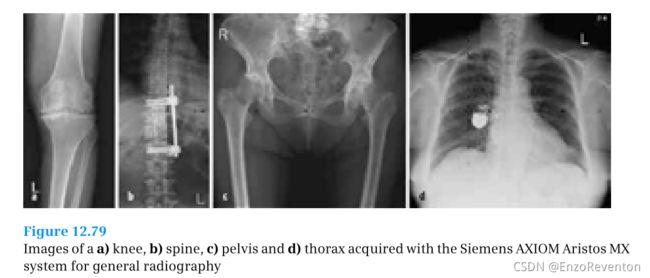
A)膝关节,b)脊柱,c)骨盆和 d)胸腔图像采集与西门子 axiom aristos mx 系统普通 x 线摄影
- Dynamic range rescaling by an appropriate setting of the grey scale window and level values: This function can be implemented automatically using the histogram of the image intensities. Additionally, image areas covered by the X-ray beam collimators can be removed. 动态范围重新标定通过适当的设置灰度窗口和水平值: 这个功能可以自动实现使用直方图的图像强度。另外,被 x 射线束准直器覆盖的图像区域可以被移除。
- Nonlinear grey scale mapping to increase contrast in the region of interest 非线性灰度制图,以增加对比度在感兴趣的区域
- Dynamic range or density compression via unsharp masking: This enables one to display a thoracic image of the lung and the mediastinum with the same high contrast. Similarly, this procedure lends itself to the simultaneous and optimal display of the breast wall and skin area of a mammogram. 动态范围或密度压缩通过反锐化掩蔽: 这使人们能够显示肺和纵隔相同的高对比度胸图像。同样,这个过程适用于乳房壁和皮肤区域的同时和最佳显示乳房 x 光片。
- Edge enhancement to enhance fine details of objects via the application of a high pass filter 通过应用高通滤波器来增强对象的细节边缘锐化
- Multifrequency filtering techniques used to combine contrast and resolution improvements with noise reduction: The image is divided into several spatial frequency domains that are separately filtered with optimized parameters. Furthermore, these parameters may adjust themselves to the local image’s signal-to-noise ratio so as to enable an optimal presentation of the diagnostic image content to the eye of the radiologist. 多频滤波技术用于结合对比度和分辨率的改善与降低噪声: 图像被划分为几个空间频率域,分别用优化的参数进行滤波。此外,这些参数可以根据当地图像的信噪比进行自我调整,从而使放射科医生的眼睛能够看到最佳的诊断图像内容。
Image stitching is a method deployed to create a new image that is larger than the detector area. A rapid examination is required in some applications (e.g. a full body scan of an elderly or weak patient in an upright position). The fast repetitive imaging capability of a flat detector allows one to take several consecutive X-ray exposures of the object with a minimal overlap between any two neighboring images. The overlapping areas of the X-ray exposures are used by the image stitching software to create seamless junctions. This enables one to display the complete spinal column or the entire skeleton in a single image.
图像拼接是一种用于创建大于探测器面积的新图像的方法。在某些应用程序中,需要进行快速检查(例如对年长或虚弱的病人进行全身扫描)。平面探测器的快速重复成像能力使得人们可以连续拍摄物体的几次 x 射线照射,而相邻两张图像之间的重叠却很小。图像拼接软件使用 x 射线曝光的重叠区域来创建无缝连接。这使得人们可以在一张图片中显示完整的脊柱或整个骨架。
The dual energy method makes use of the energy dependence of the mass absorption coefficient. Two X-ray images with very different spectra are gathered using different voltages and filters. Adequate linear superposition of the images permits one to selectively display different types of tissue. Flat detectors are ideally suited for this application because they allow one to acquire the two images rapidly and thus to reduce motion artifacts. In thoracic diagnostics, for example, soft tissue (lung parenchyma, mediastinum) or structures containing calcium (bone, calcifications) can be displayed separately, which may prove advantageous for displaying tumors. However, computed tomography is a well-established alternative to this kind of application.
双能法利用了质量吸收系数对能量的依赖关系。使用不同的电压和滤波器,收集了两幅不同光谱的 x 射线图像。所述图像的足够的线性叠加允许人们选择性地显示不同类型的组织。扁平探测器非常适合这种应用,因为它们允许一个人快速获得两个图像,从而减少运动伪影。例如,在胸部诊断中,软组织(肺实质、纵隔)或含钙结构(骨骼、钙化)可以分开显示,这对显示肿瘤是有利的。然而,X射线计算机断层成像是这种应用程序的一个广泛接受的替代方案。
平面探测器代表了将 x 射线系统集成到 ris 和 pacs 环境中的缺失环节,在这个环境中,多个组件联网以产生一个优化的工作流程。以下是建立一个通用放射摄影系统的流程所需的步骤大纲: 由区域摄影机提供的工作清单会自动载入系统的采集站。一旦从工作列表中选出病人,系统就自动选择正确的检测器(如果系统包括一个以上的检测器) ,将管和检测器定位到与第一次检测相对应的预定位置,设置发生器数据,预置管准直器,并准备采集检测器。所有必要的前后处理功能和参数也是预先选定的。所有这一切都发生在背景之前或当病人被放置在桌子上或在专门的直立立场前面。一旦拍摄了 x 光曝光照片,图像就会自动处理并立即显示在检查监视器上。同时系统自动选择各种预定义的参数,以便下一次检查工作列表。一旦获得所有的图像,它们将自动发送到 pacs,并提供给所有联网的医院科室,甚至通过远程放射学提供给远程专家。
Workflow-oriented radiography systems based on flat detectors have been shown to substantially reduce the overall times required for nearly all examinations when compared to screen-film and storage-phosphor-based systems. They thus play a central role in improving radiology department productivity.
基于平板探测器的面向工作流程的射线照相系统与屏幕-胶片和基于荧光粉的系统相比,大大减少了几乎所有检查所需的总时间。因此他们在提高放射科的生产力方面,扮演了中心角色。
Angiography and fluoroscopy 血管造影和透视
Real-time X-ray imaging systems are used for a broad spectrum of clinical applications. Such systems range from mobile X-ray systems for surgery and over- and undertable fluoroscopy systems (e.g. for examinations of the gastrointestinal tract) to angiography systems equipped for the diagnosis of vessel pathologies and minimally invasive treatment. Moreover, the field of angiography includes special systems for cardiology and neurology.
实时 x 射线成像系统用于广泛的临床应用。这些系统包括用于外科手术的可移动 x 射线系统、用于透视和透视下的系统(例如用于检查肠粘膜) ,以及用于诊断血管病变和微创治疗的血管造影系统。此外,血管造影领域包括心脏病学和神经病学的特殊系统。
Patient and user exposure to X-rays has been successively reduced along with the successive reductions in the X-ray doses required for examination and intervention. Much of this progress is due to improvements enabled by the X-ray image intensifier optical sensor combination, which still represents the gold standard for some areas in fluoroscopic X-ray imaging. All new detector technologies will have to be measured against this level of quality.
随着检查和干预所需的 x 射线剂量逐渐减少,病人和使用者接触 x 射线的机会也逐渐减少。这种进步主要归功于 x 射线图像增强器光学传感器组合的改进,它仍然代表着荧光 x 射线成像某些领域的黄金标准。所有新的探测器技术,都必须以这种质量水平来衡量。
But it has to be pointed out that the image intensifier is not perfect, mainly because of its contrast (veiling glare) and spatial resolution limitations. Furthermore, its bulkiness limits both patient access and flexibility during angulation in C-arm X-ray systems. Large-format image intensifiers have not succeeded at replacing screen-film Bucky trays in fluoroscopy systems to cover radiography applications on account of their size, round image format and limited dynamic range at the high exposure levels required in radiography. Image intensifier-based systems are also very sensitive to magnetic fields and thus cannot be used in the vicinity of high magnetic fields.
但必须指出的是,像增强器的不完善,主要是由于其对比度(面纱眩光)和空间分辨率的限制。此外,它的膨胀限制了病人接触和角度的灵活性在 c 臂 x 射线系统。大幅面影像增强器由于其体积、圆形影像格式和高曝光水平下有限的动态范围等原因,未能成功地取代荧光透视系统中的屏-胶片胶卷托盘,应用于 x 线摄影。基于像增强器的系统对磁场也非常敏感,因此不能在强磁场附近使用。
Flat detector technology has the potential to eliminate or at least reduce some of the disadvantages associated with the image intensifier. In contrast to image intensifiers, flat detectors provide
扁平检测器技术具有消除或至少减少与像增强器相关的一些缺点的潜力。与图像增强器相比,平板探测器提供
- Homogeneous image quality across the entire image area, resulting in distortion-free images and position-independent spatial resolution 整个图像区域均匀的图像质量,导致无失真图像和位置无关的空间分辨率
- High low-contrast resolution 高低对比度分辨率
- High DQE across all dose levels 所有剂量级别的药物
- Square or rectangular image areas coupled with a flat and compact design, offering improved patient access 正方形或矩形影像区加上扁平和紧凑的设计,提供改善的病人访问
- Compatibility with environments that include the use of strong magnetic fields 与环境的兼容性,包括强磁场的使用

一位新发心绞痛患者的心脏图像。A)心脏血管造影: 右冠状动脉血管次全狭窄; b)经皮介入直接支架置入术; c)介入术后无残留狭窄

两块转向磁铁的磁导航系统和一个平板探测器的 c 臂 x 射线系统(西门子 axiom artis dfc 磁导航)
These advantages suggest that X-ray systems with flat detectors may have the potential to further improve the existing applications and give way to new diagnostic and interventional techniques. The following three examples shall underline this statement.
这些优点表明,x 射线系统与平板探测器可能有潜力,进一步改善现有的应用,并让位于新的诊断和介入技术。以下三个例子将强调这一说法。
The improved detectability of small structures such as the tip of the catheter (fig. 12.80) may lead to shorter examination times. This in turn should reduce the integrated applied dose. The improved visibility of stents in cardiac angiography allows one, for instance, to use hand injections of contrast media for left ventriculograms. This reduces the contrast medium load for the patient.
小结构的可检测性的改善,例如导管的尖端(图12.80)可能导致更短的检查时间。这反过来应该减少综合应用剂量。心血管造影中支架的可见性提高,例如,可以手动注射造影剂进行左心室造影。这样可以减少病人的造影剂负荷。
The rectangular image format, high spatial resolution, distortion-free images and excellent soft-tissue contrast resolution offer advantages when it comes to applying 3D image reconstruction techniques.
矩形图像格式、高空间分辨率、无畸变图像和优秀的软组织对比度分辨率为应用三维图像重建技术提供了优势。
The flat detector’s insensitivity to magnetic fields introduces a new technology for image-guided catheter navigation in the vascular system. The tip of a special catheter is equipped with a tiny permanent magnet. Two large magnets, positioned on both sides of the patient table (fig. 12.81), generate a magnetic field at the catheter tip whose gradient can be adjusted by moving or rotating the magnets. The catheter tip can thus be maneuvered into a pre-defined direction. Guidance is provided by acquiring two X-ray images from different projections that show the catheter and the vessel structure: by drawing the new intended direction of the catheter directly onto the projection images, the new required local magnetic field can be determined and set up by moving the magnets into their new position. Difficult navigation tasks can be accomplished such as changing direction at a bifurcation, moving along a vessel with a strong bending radius and navigating other difficult sections in the vascular or cardiac system.
扁平探测器对磁场的不敏感性为血管系统中的图像导航导管引入了一种新的技术。特殊导管的顶端装有一个小永磁体。两块位于病床两侧的大型磁铁(图12.81)在导管顶端产生磁场,磁场的梯度可以通过移动或旋转磁铁来调整。因此导管顶端可以被操作到预定的方向。通过从显示导管和血管结构的不同投影中获取两个 x 射线图像来提供指导: 通过将导管的新的预期方向直接绘制到投影图像上,通过将磁铁移动到新的位置来确定和设置新的所需的局部磁场。困难的导航任务可以在分叉处改变方向,沿着弯曲半径较大的血管移动,以及在血管或心脏系统的其他困难部位导航。
The various applications of magnetic navigation center mainly on cardiac intervention. A chronic total occlusion of the cardiac vasculature, for instance, can be opened, thereby making it unnecessary for the patient to undergo cardiac surgery. Complex arrhythmia, such as fibrillation in the left atrium, can be treated via radio-frequency ablation of the arrhythmogenic tissue in the atrium. In the case of serious cardiac insufficiencies involving the use of pacemakers to stimulate both chambers of the heart, the surgeon can navigate the electrodes into optimal positions via the veins.
磁导航中心的各种应用主要是在心脏介入治疗方面。例如,慢性完全闭塞的心脏血管,可以被打开,从而使病人不必进行心脏手术。复杂的心律失常,如左心房颤动,可以通过射频消融心房的致心律失常组织来治疗。在心脏严重不足的情况下,使用起搏器刺激心脏的两个腔室,外科医生可以通过静脉导航电极到最佳位置。
12.3.4.5 Future developments 未来发展
Flat detector technology continues to develop and improve in fascinating ways. Higher bit depths of 16 or 18 bits promise improvements for 3D applications. Miniaturized electronics permit even flatter and lighter detectors for mobile and portable applications. External cooling systems, still required in some real-time applications today, may be made obsolete. Signal-to-noise ratio represents another area of improvement. Such improvements can be achieved, for instance, by extending the pixel structure into the 3rd dimension. This approach involves stacking the photodiode and switching transistors on top of one another instead of placing them next to one another in the manner of current and past designs. The active area of the photodiode is enlarged by such maximum fill-factor designs, thereby allowing one to detect nearly all of the generated photons and thus maximize the signal. The objective behind the development of new direct conversion materials (e.g. CdTe, PbI, and HgI) is to improve absorption characteristics and thus DQE.
平板探测器技术继续发展和改进,在迷人的方式。更高的16位或18位深度有望改善3 d 应用。微型电子许可证,甚至更扁平和更轻的移动和便携式应用探测器。外部冷却系统,仍然需要在一些实时应用,可能会被淘汰。信噪比是另一个需要改进的领域。这样的改进可以实现,例如,通过扩展到第三维的像素结构。这种方法包括叠加光电二极管和把晶体管一个接一个地放在一起,而不是像现在和过去的设计那样把它们一个接一个地放在一起。通过这种最大填充因子设计放大光电二极管的有效区域,从而允许人们检测几乎所有产生的光子,从而最大限度地提高信号。开发新型直接转化材料(如 CdTe、 PbI和 HgI)的目的是改善吸收特性,从而提高 DQE。
Pixel arrays based on CMOS (complementary metal oxide semiconductor) technology may provide a basis for future progress. Several steps can be envisioned. Pixel structures in the integrating domain, including a photodiode and an amplifying transistor, help to increase the signal-to-noise ratio. A further step might involve the deployment of counting structures for the detection and individual registration of each absorbed X-ray quantum. Developments of this kind would introduce the possibility of detector systems in which noise is determined only by quantum statistics. If one were to expand the counting of quanta to include the detection of their energy levels, one would be close to the development of new X-ray image contrasts based on spectral tissue properties (color imaging).
基于 CMOS (互补金属氧化物半导体)技术的像素阵列可以为未来的发展提供基础。我们可以设想几个步骤。积分域中的像素结构,包括光电二极管和放大晶体管,有助于提高信噪比。进一步的步骤可能涉及部署计数结构,用于检测和单独登记每个吸收的 x 射线量子。这种发展将引入仅由量子统计决定噪声的探测器系统的可能性。如果扩大量子计数的范围,包括探测它们的能级,那么将接近基于光谱组织特性(彩色成像)的新 x 射线图像对比的发展。

