传输门、D 锁存器、D触发器、建立时间与保持时间
TRANSMISSION GATE,D LATCH,DFF,SETUP &HOLD
-
- Remark:plysicaldesign4u
- Transmission Gate
- D latch(时钟电平触发)
-
- Positive D latch using transmission Gate
- Negative D latch using transmission Gate
- D Flip flop(时钟边沿触发)
-
- D Flip flop using a transmission gate
- Setup Time
-
- If skew is present in the design
- Hold Time
-
- If positive skew is present
- If negative skew is present
Remark:plysicaldesign4u
在了解setup time和hold time之前,我们应该了解D锁存器D latch和 D触发器DFF 。D锁存器和DFF是由传输门transmission gate和反相器inverters组成。
Transmission Gate
- The transmission gate is consists of a parallel connection of PMOS & NMOS.
- Two gate voltage of PMOS and NMOS are the complement of each other.
- The effective resistance of the transmission gate is almost constant because of the parallel connection of PMOS and NMOS.
- It is a bidirectional circuit and it carries the current in either direction.(这是一个双向电路,它把电流传送到任何一个方向)
PMOS is on when gate input is 0. NMOS is on when gate input is 1.

When control is high (1) from the truth table we can see both transistors are ON at the same time and whatever is applied to the input we got at the output.
When control is low (0) from the truth table we can see both transistors are OFF at the same time and whatever is applied to the input is not reached to the output so we got high impedance (Z) at the output.
D latch(时钟电平触发)
The latch is a level-sensitive(电平敏感) device and it is transparent when the clock is high if it is a positive level-sensitive latch and when the clock is low it is called negative level-sensitive latch.
In latch the output (Q) is dependent only on the level of the clock (Clk). In this latch D is control the output (Q).

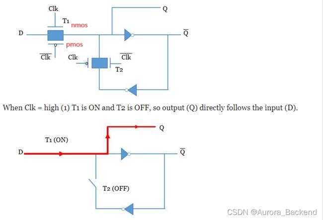
Positive D latch using transmission Gate
- It consists of two transmission gates and two inverters.

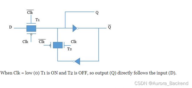
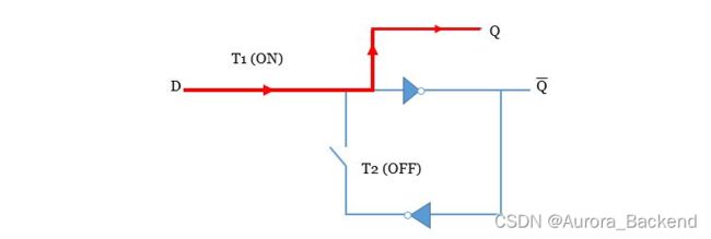
Negative D latch using transmission Gate
It is also consist of two transmission gate and two inverters. It is working in an exactly opposite manner of the positive level-sensitive D latch.
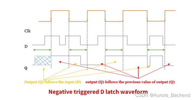
- When Clk = high (1) T1 is OFF and T2 is ON, now new data entering into the latch is stopped and we get only previously-stored data at the output

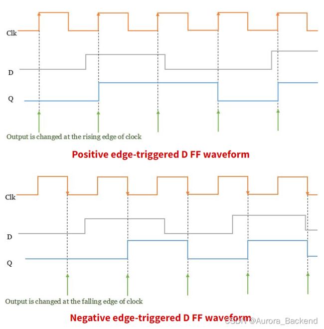
D Flip flop(时钟边沿触发)
A D flip flop is an edge-triggered边沿触发 device which means the output (Q) follows the input (D) only at the active edge (for positive rising edge) of the clock (for the positive edge-triggered) and retain the same value until the next rising edge i.e. output does not change between two rising edges, it should be changed only at the rising edge.
输出Q仅在时钟的上升沿(对于上升沿触发)跟随输入D ,并保持相同的值,直到下一个上升沿,即输出不会在两个上升沿之间改变,它应该只在上升边沿改变。

- 上升沿触发与下降沿触发的D触发器
D Flip flop using a transmission gate
It is a combination of negative level-sensitive latch and positive level-sensitive latch that giving an edge-sensitive
device. Data is change only at the active edge of the clock.(data只在有效的时钟边沿改变)


-
when Clk= Low (0) T1, T4 is ON and T2, T3 is OFF.
-
New data (D) is continuously entering through T1 and getting stored till the edge of
T2 (path is D-1-2-3-4 and at node 4 it stops)it cannot pass through T2 and T3 transmission gate because they are off. This operation for the master latch. -
For slave latch it keeps retaining the previously stored value of output (Q) (path is 5-6-7-8-5).(保持的是以前存储的输出值)

-
When Clk= HIGH (1) T2, T3 are ON and T1, T4 are OFF.
-
Now master latch did not allow new data to enter into the device because T1 is OFF and the previously stored data at point 4 is going through the path 4-1-2-5-6-Q and this same data is reflected at the output and this does not change until the next rising edge and this same data is also going to the transmission gate T4 (path is 4-1-2-5-6-7-8 and stops because transmission gate T4 is OFF).
Again if Clk is low the master latching circuit is enabled and there is no change in the output.
Any changes in input is reflected at node 4 which is reflected at the output at the next positive edge of the clock.
输入的任何变化都会反映在“节点 4”上,并会在时钟的下一个上升沿反映在输出上。
So we can say that if D changes, the changes would reflect only at node 4 when the clock is low and it will appear at the output only when the Clk is high.
如果 D发生变化,则D的变化只会在时钟为低电平时反映在节点 4 上,只有在 Clk 为高电平时D的变化才会出现在输出端。
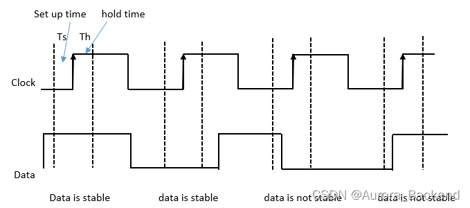
Setup Time
The minimum time for which the data (D) should be stable at the input before the active edge of clock arrival.
The data is launched from FF1 and captured at the FF2 at the next clock edge. The launched data should be present at the D pin of capture flop at least setup time before the next active edge of the clock arrives.
launched data应至少在时钟的下一个有效沿到达之前的建立时间前出现在捕获触发器capture flop的 引脚上。

So total time to propagate the data(传播数据的总时间) from launch to capture flop = one time period (T) –Tsu
This is the required time for the data travel from launch to capture flop.
And how much time it does take data to arrive at the D pin of capture flop is =Tcq (clock to Q delay of FF1) + Tcomb (combinational delay). This is called arrival time.
So condition for setup timing to not violate
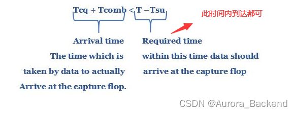
- Require time > Arrival time
- Slack = Require time - Arrival time
- Slack > 0 (no violation)
- Slack < 0 (setup violation)
PR阶段对于setup是否需要fix的判断方法是slack是否小于100ps(-100ps以内都可以)
WNSworst negative slack控制在100ps以内就可以往下继续跑其他flow,这里是指PR阶段即ICC2或Innovus中。PR实现过程是一个实现的过程,而非timing signoff或时序验收阶段。PR这个过程可以理解成工地里面的施工队,而PT是第三方验收单位。工程合不合格需要看PT第三方验收结果。但是为了达到某个特定要求的验收标准,施工队PR就得按照稍微高点的标准来施工,这样验收的时候才能更容易通过(严于律己)。

-
setup time
- When the CLK is low the input (D) is following the path D-1-2-3-4 and it will take some time to reach at the node 4 that time we will call setup time.
-
如果在时钟的下一个有效边沿到达之前,data (D) is not stable for the setup time,会发生什么
- So now when the clock turns high the data which has to be launched should be present at node 4
- but since the data is slow it would not get enough time to travel till node 4 and the data (D) is still be present somewhere between node 2 and 3 (let’s say) 由于数据很慢,它没有足够的时间传输到节点4,而数据(D)仍然出现在节点2和3之间的某个地方
- so we don’t know which data will be launched at the rising edge and output will be indeterminate(不确定的) because data is not reached at node 4. Data is late.
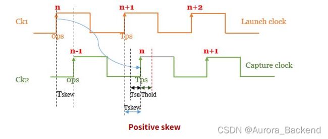
If skew is present in the design

If there is a positive skew it means we are giving more time to data to arrive at D pin of capture FF. so positive skew is good for setup but bad for hold
Tskew is positive or negative depending on the capture clock it comes fast or slow than the launch clock.
- Positive skew: if the capture clock comes late than the launch clock.
- Negative skew: if the capture clock comes early than the launch clock.
Hold Time
The minimum time for which the data (D) should be stable at the input after the active edge of clock has arrived.

- Data is launched from FF1 at osec and this data should be captured at FFF2 after one time period (T).
- The hold time is to make sure that the current data (n) which is being captured at the FF2 should not be corrupted(破坏) by the next data (n+1) which has been launched from the launch flop at the same edge(不会被从同一边沿发射的下一个数据(n + 1)破坏)
Why do we check to hold at the same edge itself?
-
Because this same edge is going to both the flip flops if at this edge The capturing flop FF2 is capturing the current data (n) at this same edge itself the launch flop FF1 is launching the next data (n+1)
-
so the whole check is to make sure that this new data (n+1) which is being launched at the same edge from the launch flop FF1 should not come so fast that it corrupts the current data (n) which is being captured at the capture flop at the same edge.
The arrival time of this (n+1)th data should at least be greater(更长) than the Thold time of capture flop FF2.
Basically this current data (n) should be held for enough time for it to be captured reliably, that enough time is called hold time.

-
Hold slack = Arrival time – Require time
- Hold slack > 0 (No violation)
- Hold slack < 0 (hold violation)
-
If arrival time is less that means data coming is very fast (or early) so hold violation occurs
If positive skew is present
It means the next data (n+1) will be launched early from the launch flop FF1 and till now the capture clock is not reached to the capture flop FF2 so the data (n) also did not have to capture yet,
but this nth(第n个数据) data has to be stable at the capture clock for Tskew+ Thold time otherwise data n will be corrupted.
So we can say positive skew is bad for hold.(hold slack = arriveal time - require time变大了)
If negative skew is present
it means the data (n) is being captured at captured flop FF2 early but by the time (n+1) data will not be getting launched from the launched flop FF1,
so the data (n) got enough time to be held at the input for it to be captured reliability but till now the launch flop did not launch (n+1) data. So negative skew is good for hold.
