ARTS 挑战打卡的第5天 --- 实现简单的 1.2V 电机控制设计(Share)
前言
(1)在逛嵌入式社区的时候,突然发现了这一篇博客挺有意思的。如果是想做电动牙刷的朋友可以看看。
(2)原文链接:https://www.embedded.com/implementing-a-simple-1-2v-motor-control-design/
Implementing a simple 1.2V motor control design(实现简单的 1.2V 电机控制设计)
introduction (前言)
During the last decade, oral health and hygiene were given special attention. This tendency is driving more innovation among designers who invent new enhanced oral health technologies. Electric toothbrushes significantly improved the brushing experience and brushing habits.
在过去的十年中,口腔健康和卫生受到特别关注。这种趋势正在推动发明新的增强口腔健康技术的设计师进行更多创新。电动牙刷显着改善了刷牙体验和刷牙习惯。
The most popular and effective type of electric toothbrush is the one with a rotating or side-to-side movement. Motions at sonic or lower speeds are made thanks to a motor.
最流行和最有效的电动牙刷类型是旋转或左右移动的电动牙刷。电机可以实现音速或更低速度的运动。
Modern electric toothbrushes typically rely on rechargeable batteries, which are charged through inductive charging when the toothbrush is placed in a charging base between uses. They often use nickel-metal hydride (NiMH) batteries, whose nominal voltage is 1.2 V. The Low Voltage GreenPAK™ SLG47513 has a working voltage range from 1 V to 1.65 V, enabling control over the toothbrush’s operation.
现代电动牙刷通常使用可充电电池,当牙刷被放置在充电底座上时,通过感应充电来充电。他们通常使用镍氢(NiMH)电池,其标称电压为1.2 V。低电压GreenPAK™SLG47513的工作电压范围从1 V到1.65 V,可以控制牙刷的操作。
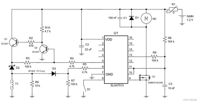
Figure 1: General schematic of electric toothbrush based on SLG47513.
图1:基于SLG47513的电动牙刷的总体原理图。
GreenPAK Design(总体设计)
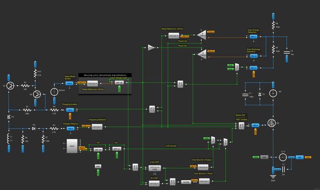
Figure 2 shows an internal design of the electric toothbrush in Go Configure™ Software Hub. The complete design file can be found here: AN-CM-360 Electric Toothbrush.gp6.
图 2 显示了 GoConfigure™ Software Hub 中电动牙刷的内部设计。完整的设计文件可以在这里找到:AN-CM-360电动牙刷.gp6
Figure 2: Electric toothbrush GreenPAK designer schematic.
图 2:电动牙刷 GreenPAK 设计器原理图。
Motor Control(电机控制)
When the toothbrush is in sleep mode, Pin 8 output is set to HIGH due to a pull-up resistor, but when a button is pressed, a low-level signal appears for a brief period. To filter out switch bouncing, a Delay macrocell DLY4 is used.
当牙刷处于睡眠模式时,由于上拉电阻,第 8 脚输出被设置为高电平,但当按下按钮时,会出现短暂的低电平信号。为了滤除开关跳动,使用了延迟宏单元 DLY4。
A DFF18 latches the voltage level and flips it each time the button is pressed, allowing the toothbrush to switch between two modes using an external button – working mode and sleep mode.
DFF18 会锁存电压电平,并在每次按下按钮时翻转它,从而允许牙刷使用外部按钮在两种模式之间切换:工作模式和睡眠模式。
When the toothbrush is switched to the working mode, there is a constant HIGH voltage level at a gate of a transistor, as well as at the output of a multiplexer 3-L2. This voltage level opens the transistor Q3 and starts a DC motor.
当牙刷切换到工作模式时,晶体管的栅极以及多路复用器3-L2的输出端有恒定的高电压电平。该电压电平打开晶体管 Q3 并启动直流电机。
The brush has 2 timers. The first one informs the user about the completion of a 2-minute brushing session. An oscillator OSC0, a DFF19, and a DFF11 form a clock signal with a frequency of 2.67 Hz.
刷子有 2 个定时器。第一个通知用户 2 分钟的刷牙过程已完成。振荡器OSC0、DFF19和DFF11形成频率为2.67Hz的时钟信号。
When the toothbrush is switched to ON mode, a 2-bit LUT1 feeds this clock signal to the CLK input of a CNT0. After two minutes have passed, a HIGH level appears at the CNT0 output, which triggers a one-shot (CNT6), forming a signal pulse with a width equal to three and a half periods of the clock signal.
当牙刷切换到 ON 模式时,2 位 LUT1 将此时钟信号馈送到 CNT0 的 CLK 输入。两分钟后,CNT0 输出出现高电平,触发单触发(CNT6),形成宽度等于时钟信号三个半周期的信号脉冲。
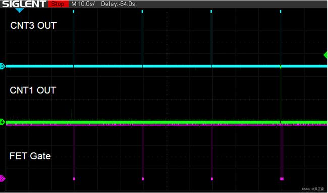
These three pulses, through two multiplexers, 3-bit LUT0, and Pin 9 are fed to the transistor gate and, accordingly, to the motor, creating a vibration effect (see Figure 3 and Figure 4a).
这三个脉冲通过两个多路复用器、3 位 LUT0 和引脚 9 馈送到晶体管栅极,并相应地馈送到电机,从而产生振动效果(见图 3 和图 4a)。
In addition to the 2-minute timer, this toothbrush also contains a 30-second timer based on a CNT3, which signals the need to proceed with brushing the next quadrant (quarter) of the oral cavity. After 30 seconds have passed, a HIGH level appears at the CNT3 output.
除了 2 分钟计时器外,这款牙刷还包含一个基于 CNT3 的 30 秒计时器,该计时器发出信号,表明需要继续刷牙口腔的下一个象限(四分之一)。 30 秒后,CNT3 输出出现高电平。
A 2-bit LUT0 filters every 4th pulse, and a Filter macrocell eliminates glitches. The CNT3 output signal triggers a one-shot (CNT1), which forms a signal pulse with a width equal to one and a half periods of the clock signal (see Figure 3 and Figure 4b).
2 位 LUT0 每 4 个脉冲进行一次过滤,过滤器宏单元可消除毛刺。 CNT3 输出信号触发单触发 (CNT1),形成宽度等于时钟信号一个半周期的信号脉冲(见图 3 和图 4b)。
To ensure that the timers are restarted each time the toothbrush is turned off, the counters are reset on the rising edge of the DFF18 output signal.
为了确保每次关闭牙刷时计时器都会重新启动,计数器会在 DFF18 输出信号的上升沿重置。
Digital multiplexers enable the passage of either a constant voltage, one pulse, or three pulses to the transistor gate based on the one-shots outputs.
数字多路复用器可根据单次输出将恒定电压、一个脉冲或三个脉冲传递到晶体管栅极。
The 3-bit LUT0 prevents the motor from running while charging. Specifically, a signal on the transistor gate is HIGH only when the toothbrush is in working mode and not placed in the charging station.
3 位 LUT0 可防止电机在充电时运行。具体地,仅当牙刷处于工作模式并且未放置在充电站中时,晶体管栅极上的信号才为高电平。
Figure 3: Waveforms that illustrate work of toothbrush during one brushing session .
图 3:说明一次刷牙过程中牙刷工作情况的波形。
Figure 4: Signals informing about completion: 2-minute total brushing (left) and 30-second quadrant brushing (right).
图 4:通知完成的信号:总刷牙时间为 2 分钟(左)和象限刷牙时间为 30 秒(右)。
Charging(充电)
Most modern electric toothbrushes use wireless inductive charging. The toothbrush and its base form a two-part transformer, with the base having the primary winding of the transformer and the toothbrush having the secondary winding.
大多数现代电动牙刷都使用无线感应充电。牙刷及其底座形成两部分变压器,底座具有变压器的初级绕组,牙刷具有次级绕组。
The voltage induced on the secondary winding is rectified by a diode D1 and then reduced by a resistive divider to the value required for proper detection of the presence of a charger (see Figure 1).
次级绕组上感应的电压通过二极管 D1 进行整流,然后通过电阻分压器降低至正确检测充电器是否存在所需的值(见图 1)。
The divider comprises external resistors R7 (100 kΩ) and R5 (4.7 kΩ), and an internal pull-down resistor (10 kΩ) inside the SLG47513, which sets the peak value of the voltage on Pin 6 at around 1.2 V.
该分压器包括外部电阻器 R7 (100 kΩ) 和 R5 (4.7 kΩ),以及 SLG47513 内部的内部下拉电阻器 (10 kΩ),它将引脚 6 上的电压峰值设置在 1.2 V 左右。
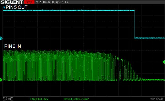
When the signal from the charger reaches Pin 6, which functions as an analog comparator, a HIGH level appears at the input of a frequency detector.
当来自充电器的信号到达用作模拟比较器的引脚 6 时,频率检测器的输入端会出现高电平。
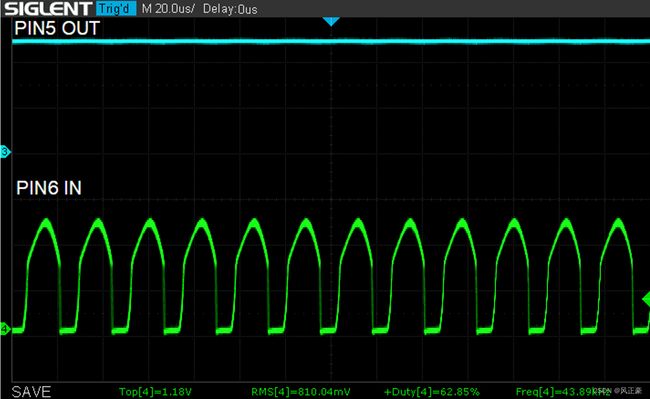
The frequency detector generates a high-level output on this signal, which goes to Pin 5 and enables charging (see Figure 5 and Figure 6).
频率检测器在此信号上生成高电平输出,该信号发送到引脚 5 并启用充电(参见图 5 和图 6)。
This high-level signal at the output of Pin 5 opens a Q2 transistor, which, in turn, opens a Q1 transistor, initiating the charging process of the battery.
引脚 5 输出处的高电平信号会打开 Q2 晶体管,进而打开 Q1 晶体管,启动电池的充电过程。
Figure 5: Signal from charger at input of pin 6 and output enable at pin 5.
图 5:引脚 6 输入处来自充电器的信号和引脚 5 处输出使能的信号。
Figure 6: Signals at input of pin 6 and output of pin 5 during the process of disconnecting charger.
图 6:断开充电器过程中引脚 6 输入和引脚 5 输出的信号。
To protect the battery against overcharging, an analog comparator ACMP1H is used. Resistors R8 and R9 divide the battery voltage in half, and this voltage is applied to the input of Pin 11. Then it is compared with a reference voltage of 725 mV by a comparator with a hysteresis of 100 mV.
为了防止电池过度充电,使用了模拟比较器 ACMP1H。电阻R8和R9将电池电压分成两半,并将该电压施加到引脚11的输入。然后通过迟滞为100 mV的比较器将其与725 mV的参考电压进行比较。
If the voltage from the divider reaches this reference voltage, the battery charging stops. A Delay macrocell DLY2 as a filter is used.
如果分压器的电压达到该参考电压,电池充电就会停止。使用延迟宏单元DLY2作为滤波器。
To protect the battery against over-discharging, an analog comparator ACMP0H is used. This comparator compares the same voltage from the divider but has its reference voltage set at 500 mV and hysteresis at 100 mV.
为了防止电池过度放电,使用了模拟比较器 ACMP0H。该比较器比较来自分压器的相同电压,但其参考电压设置为 500 mV,迟滞设置为 100 mV。
When the measured voltage becomes less than the reference, the comparator output goes LOW and the transistor closes, preventing the battery from over-discharging.
当测量的电压低于参考电压时,比较器输出变为低电平,晶体管关闭,防止电池过度放电。
To prevent the circuit from consuming excess energy through the divider, the divider is connected to the ground bus only when the battery is charging or when the toothbrush is on.
为了防止电路通过分压器消耗过多的能量,仅当电池充电或牙刷打开时,分压器才连接到接地总线。
These conditions are checked by a 2-bit LUT3 and its output goes HIGH when at least one of the conditions is met. A multiplexer 3-L0, based on this high-level signal, connects the ground bus to the divider through an open-collector transistor of Pin13. Additionally, ACMP0H is powered on only when the toothbrush comes out of sleep mode, and ACMP1H is powered on only when the charger is connected.
这些条件由 2 位 LUT3 检查,当至少满足其中一个条件时,其输出变为高电平。多路复用器 3-L0 根据该高电平信号,通过 Pin13 的集电极开路晶体管将接地总线连接到分压器。此外,ACMP0H 仅当牙刷退出睡眠模式时才通电,ACMP1H 仅当连接充电器时才通电。
These measures ensure extremely low consumption in sleep mode.
这些措施可确保睡眠模式下的功耗极低。
Simulation of Project(项目模拟)
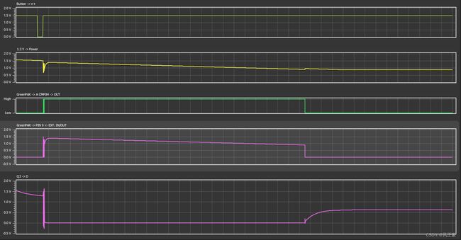
The motor control part of the project can be simulated in the GreenPAK Designer Software Simulation Tool. Figure 7 shows simulation waveforms. The simulation shows that after pressing the button, the transistor opens and the motor starts working.
该项目的电机控制部分可以在GreenPAK Designer软件仿真工具中进行仿真。图 7 显示了仿真波形。仿真表明,按下按钮后,晶体管打开,电机开始工作。
And when the battery voltage becomes less than 900 mV, the motor turns off.
当电池电压低于 900 mV 时,电机关闭。
Figure 7: Simulation waveforms for motor control part.
图 7:电机控制部分的仿真波形。
Conclusions (结论)
The SLG47513 low-voltage operation allows to power the proposed device by just one 1.2 V NiMH battery, which is the primary power source for electric toothbrushes.
SLG47513 低压运行允许仅通过一节 1.2 V NiMH 电池为拟议设备供电,这是电动牙刷的主要电源。
The SLG47513 is a perfect fit for these devices as it has enough digital and analog macrocells that can be used to control the toothbrush motor and implement additional features such as timers and charging control.
SLG47513 非常适合这些设备,因为它具有足够的数字和模拟宏单元,可用于控制牙刷电机并实现定时器和充电控制等附加功能。
The SLG47513 can serve as a functional replacement for popular electric toothbrushes available in the market.
SLG47513 可作为市场上流行电动牙刷的功能替代品。
Because there are not many integrated circuits available in the market that can be powered by 1.2 V and can implement toothbrush functionalities, manufacturers often use custom ASICs, which increases the cost of the toothbrush.
由于市场上可用1.2V供电并能实现牙刷功能的集成电路并不多,制造商通常使用定制ASIC,这增加了牙刷的成本。
GreenPAK is a cost-effective solution as it uses an off-the-shelf base die and comes in an extremely small case of 1.6 mm x 1.6 mm, which helps to reduce the board space required.
GreenPAK 是一种经济高效的解决方案,因为它使用现成的基础芯片,并且采用 1.6 mm x 1.6 mm 的极小外壳,有助于减少所需的电路板空间。
Note: All images are courtesy of Renesas Electronics.
注:所有图片均由瑞萨电子提供。
