Enable Secure boot on software
User Guide:
- Secure Boot V1
- Secure Boot V2
- espsecure.py
Please follow these steps:
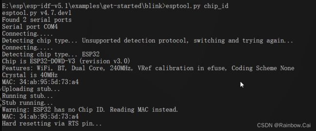
1、Query the chip version
esptool.py chip_id
-
The V1.0 version chip only supports Secure boot V1
-
The V3.0 or later version chip support Secure boot V2
2、You need to get the secure boot private key. As follows:
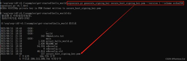
- The Secure Boot V1 key requires use the
ECDSA 256(SHA-256) bitprivatekeys.
- Running the following command to obtain the Secure Boot V1
ECDSA 256bit(SHA-256) private key.
espsecure.py generate_signing_key secure_boot_signing_key.pem --version 1 --scheme ecdsa256
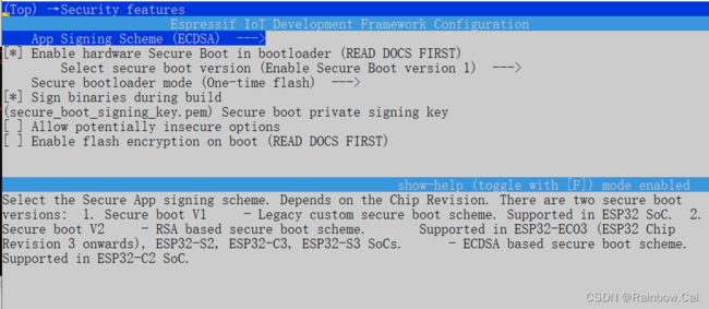
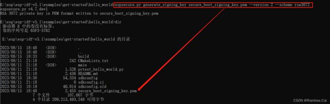
- If you are use the
ECO3orECO4SoC , we recommend to use the Secure Boot V2 . The Secure boot V2 key requires use thersa3072private keys. - To use
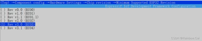
Secure boot v2, need to set the chip version toECO3orECO4, as follows:
Component config → Hardware Settings → Chip revision → Minimum Supported ESP32 Revision
- Running the following command to obtain the
secure boot V2key.
espsecure.py generate_signing_key secure_boot_signing_key.pem --version 2 --scheme rsa3072
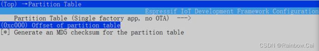
3、You need to increase the partition table address Settings.
Since enable secure boot will increases the size of the bootloader.bin firmware, so the offset of the default partition table needs to be adjusted, which is 0x8000, can be adjusted to 0xc000. You can modify the settings for partition table in menuconfig. As follows:
4、You need to enable secure boot config on software
- Please set the correct private key file(
secure_boot_signing_key.pem)

5、To get the bootloadr.bin and download the bootloadr.bin
- Running the follows command to
getthebootloadr.bin
idf.py bootloader
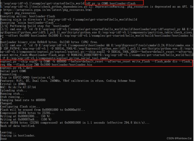
- Running the follows command to
downloadthebootloadr.bin
idf.py -p COM6 bootloader-flash
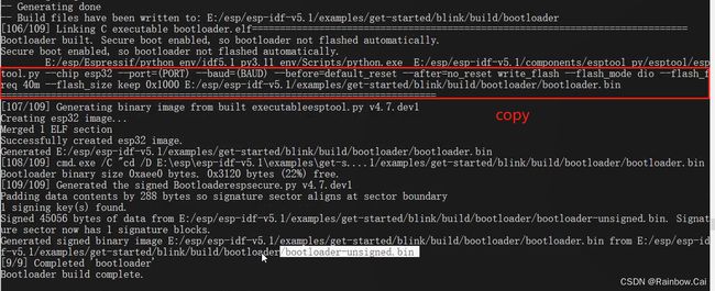
- You can also use the follows command to download the bootloadr.bin
esptool.py --chip esp32 --before=default_reset --after=no_reset write_flash --flash_mode dio --flash_freq 40m --flash_size keep 0x1000 E:/esp/esp-idf-v5.1/examples/get-started/blink/build/bootloader/bootloader.bin
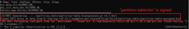
6、 To compile the firmware
- Then , Running the following command to compile the firmware and get the
partition-table.binandapp.bin. As follows:
idf.py build
- If you are using the
secure boot V1, After compiled, you will get the signed firmware and a summary of the public key generated based on the secure boot signature private key.- The
partition-table.binandapp.binwill be signed, thebootloader.binfirmware will not be signed. As follows:
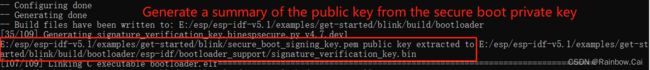
- A summary of the public key generated based on the secure boot signature private key
- The
-
If you are using the
secure boot V2,After compiled, you will get the signed firmware- The
app.binandbootloade.binwill be signed, thepartition tablefirmware will not be signed.
- The
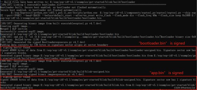
- When use the secure boot private key(secure_boot_signing_key.pem) to sign the plaintext firmware, the public key and the summary of the public key will are generated. The public key and the summary of the public key will storage to the signature block. The signature block is written at the end of the firmware.
7、To download the signed partition-table.bin and signed app.bin and monitor the running log.
- Running the following command to download the signed
partition-table.binand signedapp.binand monitor the running log.
idf.py flash monitor

After the firmware is downloaded, the secure boot will be enabled when the first boot. You can confirm the secure boot process by viewing the running log . As follows:

You can running the “espefuse.py -p COM4 summary” command to query eFuse information, and you can seen secure boot is enabled.
espefuse.py summary
espefuse.py v4.7.dev1

A fatal error occurred: Could not open /dev/ttyUSB0, the port doesn't exist
Please make sure that you have specified the right port with the --port argument

E:\esp\esp-idf-v5.1\examples\get-started\blink>espefuse.py -p COM4 summary
espefuse.py v4.7.dev1
Connecting......
Detecting chip type... Unsupported detection protocol, switching and trying again...
Connecting....
Detecting chip type... ESP32

=== Run "summary" command ===
EFUSE_NAME (Block) Description  = [Meaningful Value] [Readable/Writeable] (Hex Value)
----------------------------------------------------------------------------------------
Calibration fuses:
ADC_VREF (BLOCK0)                                  True ADC reference voltage                         = 1114 R/W (0b00010)

Config fuses:
WR_DIS (BLOCK0)                                    Efuse write disable mask                           = 256 R/W (0x0100)
RD_DIS (BLOCK0)                                    Disable reading from BlOCK1-3                      = 2 R/W (0x2)
DISABLE_APP_CPU (BLOCK0)                           Disables APP CPU                                   = False R/W (0b0)
DISABLE_BT (BLOCK0)                                Disables Bluetooth                                 = False R/W (0b0)
DIS_CACHE (BLOCK0)                                 Disables cache                                     = False R/W (0b0)
CHIP_CPU_FREQ_LOW (BLOCK0)                         If set alongside EFUSE_RD_CHIP_CPU_FREQ_RATED; the = False R/W (0b0)
                                                    ESP32's max CPU frequency is rated for 160MHz. 24
                                                   0MHz otherwise
CHIP_CPU_FREQ_RATED (BLOCK0)                       If set; the ESP32's maximum CPU frequency has been = True R/W (0b1)
                                                    rated
BLK3_PART_RESERVE (BLOCK0)                         BLOCK3 partially served for ADC calibration data   = False R/W (0b0)
CLK8M_FREQ (BLOCK0)                                8MHz clock freq override                           = 50 R/W (0x32)
VOL_LEVEL_HP_INV (BLOCK0)                          This field stores the voltage level for CPU to run = 0 R/W (0b00)
                                                    at 240 MHz; or for flash/PSRAM to run at 80 MHz.0
                                                   x0: level 7; 0x1: level 6; 0x2: level 5; 0x3: leve
                                                   l 4. (RO)
CODING_SCHEME (BLOCK0)                             Efuse variable block length scheme
   = NONE (BLK1-3 len=256 bits) R/W (0b00)
CONSOLE_DEBUG_DISABLE (BLOCK0)                     Disable ROM BASIC interpreter fallback             = True R/W (0b1)
DISABLE_SDIO_HOST (BLOCK0)                                                                            = False R/W (0b0)
DISABLE_DL_CACHE (BLOCK0)                          Disable flash cache in UART bootloader             = False R/W (0b0)

Flash fuses:
FLASH_CRYPT_CNT (BLOCK0)                           Flash encryption is enabled if this field has an o = 0 R/W (0b0000000)
                                                   dd number of bits set
FLASH_CRYPT_CONFIG (BLOCK0)                        Flash encryption config (key tweak bits)           = 0 R/W (0x0)

Identity fuses:
CHIP_PACKAGE_4BIT (BLOCK0)                         Chip package identifier #4bit                      = False R/W (0b0)
CHIP_PACKAGE (BLOCK0)                              Chip package identifier                            = 1 R/W (0b001)
CHIP_VER_REV1 (BLOCK0)                             bit is set to 1 for rev1 silicon                   = True R/W (0b1)
CHIP_VER_REV2 (BLOCK0)                                                                                = False R/W (0b0)
WAFER_VERSION_MINOR (BLOCK0)                                                                          = 0 R/W (0b00)
WAFER_VERSION_MAJOR (BLOCK0)                       calc WAFER VERSION MAJOR from CHIP_VER_REV1 and CH = 1 R/W (0b001)
                                                   IP_VER_REV2 and apb_ctl_date (read only)
PKG_VERSION (BLOCK0)                               calc Chip package = CHIP_PACKAGE_4BIT << 3 + CHIP_ = 1 R/W (0x1)
                                                   PACKAGE (read only)

Jtag fuses:
JTAG_DISABLE (BLOCK0)                              Disable JTAG                                       = True R/W (0b1)

Mac fuses:
MAC (BLOCK0)                                       MAC address
   = fc:f5:c4:4c:07:cc (CRC 0xc1 OK) R/W
MAC_CRC (BLOCK0)                                   CRC8 for MAC address                               = 193 R/W (0xc1)
MAC_VERSION (BLOCK3)                               Version of the MAC field                           = 0 R/W (0x00)

Security fuses:
UART_DOWNLOAD_DIS (BLOCK0)                         Disable UART download mode. Valid for ESP32 V3 and = False R/W (0b0)
                                                    newer; only
ABS_DONE_0 (BLOCK0)                                Secure boot V1 is enabled for bootloader image     = True R/W (0b1)
ABS_DONE_1 (BLOCK0)                                Secure boot V2 is enabled for bootloader image     = False R/W (0b0)
DISABLE_DL_ENCRYPT (BLOCK0)                        Disable flash encryption in UART bootloader        = False R/W (0b0)
DISABLE_DL_DECRYPT (BLOCK0)                        Disable flash decryption in UART bootloader        = False R/W (0b0)
KEY_STATUS (BLOCK0)                                Usage of efuse block 3 (reserved)                  = False R/W (0b0)
SECURE_VERSION (BLOCK3)                            Secure version for anti-rollback                   = 0 R/W (0x00000000)
BLOCK1 (BLOCK1)                                    Flash encryption key
   = 00 00 00 00 00 00 00 00 00 00 00 00 00 00 00 00 00 00 00 00 00 00 00 00 00 00 00 00 00 00 00 00 R/W
BLOCK2 (BLOCK2)                                    Security boot key
   = ?? ?? ?? ?? ?? ?? ?? ?? ?? ?? ?? ?? ?? ?? ?? ?? ?? ?? ?? ?? ?? ?? ?? ?? ?? ?? ?? ?? ?? ?? ?? ?? -/-
BLOCK3 (BLOCK3)                                    Variable Block 3
   = 00 00 00 00 00 00 00 00 00 00 00 00 00 00 00 00 00 00 00 00 00 00 00 00 00 00 00 00 00 00 00 00 R/W

Spi Pad fuses:
SPI_PAD_CONFIG_HD (BLOCK0)                         read for SPI_pad_config_hd                         = 0 R/W (0b00000)
SPI_PAD_CONFIG_CLK (BLOCK0)                        Override SD_CLK pad (GPIO6/SPICLK)                 = 0 R/W (0b00000)
SPI_PAD_CONFIG_Q (BLOCK0)                          Override SD_DATA_0 pad (GPIO7/SPIQ)                = 0 R/W (0b00000)
SPI_PAD_CONFIG_D (BLOCK0)                          Override SD_DATA_1 pad (GPIO8/SPID)                = 0 R/W (0b00000)
SPI_PAD_CONFIG_CS0 (BLOCK0)                        Override SD_CMD pad (GPIO11/SPICS0)                = 0 R/W (0b00000)

Vdd fuses:
XPD_SDIO_REG (BLOCK0)                              read for XPD_SDIO_REG                              = False R/W (0b0)
XPD_SDIO_TIEH (BLOCK0)                             If XPD_SDIO_FORCE & XPD_SDIO_REG                   = 1.8V R/W (0b0)
XPD_SDIO_FORCE (BLOCK0)                            Ignore MTDI pin (GPIO12) for VDD_SDIO on reset     = False R/W (0b0)

Flash voltage (VDD_SDIO) determined by GPIO12 on reset (High for 1.8V, Low/NC for 3.3V)