赛灵思的block memory generator用户手册pg058翻译和学习(AXI4 Interface Block Memory Generator Feature Summary)
(1)
读赛灵思IP手册,block memory generator Product Guide,即内存memory系列(如RAM ROM等)的手册。本期介绍AXI4 Interface Block Memory Generator Feature Summary(1)AXI4接口BMG功能概述(1)。
P10
AXI4 Interface Block Memory Generator Feature Summary
AXI4接口BMG功能概述
Overview
AXI4 Interface Block Memories are built on the Native Interface Block Memories (see Figure 1-1). Two AXI4 interface styles are available: AXI4 and AXI4-Lite. The core can also be further classified as a Memory Slave or as a Peripheral Slave. In addition to applications supported by the Native Interface Block Memories, AXI4 Block Memories can also be used in AXI4 System Bus applications and Point-to-Point applications.
概述
AXI4接口块存储器建立在本地(Native)接口块存储器上(见图1-1)。有两种AXI4接口样式可用:AXI4和AXI4Lite。内核还可以进一步分类为内存从机或外设从机。除了本机接口块存储器支持的应用程序外,AXI4块存储器也可用于AXI4系统总线应用程序和点对点应用程序。
All communication in the AXI protocol is performed using five independent channels. Each of the five independent channels consists of a set of information signals and uses a two-way valid and ready handshake mechanism. The information source uses the valid signal to show when valid data or control information is available on the channel. The information destination uses the ready signal to show when it can accept the data.
AXI协议中的所有通信都使用五个独立的信道进行。五个独立信道中的每一个都由一组信息信号组成,并使用双向有效且就绪的握手机制。信息源使用有效信号来显示信道上何时有有效数据或控制信息可用。信息目的地使用就绪信号来显示何时可以接收数据。
In Figure 1-2, the information source generates the valid signal to indicate when data is available. The destination generates the ready signal to indicate that it can accept the data, and transfer occurs only when both the valid and ready signals are High.
在图1-2中,信息源生成有效信号以指示数据何时可用。目的地生成就绪信号以指示它可以接受数据,并且只有当有效信号和就绪信号都为高时才发生传输。
The AXI4 Block Memory Generator core is an AXI4 endpoint Slave IP and can communicate with multiple AXI4 Masters in an AXI4 System or with Standalone AXI4 Masters in point to point applications. The core supports Simple Dual-Port RAM configurations. Because AXI4 Block Memories are built using Native interface Block Memories, they share many common features.
AXI4块内存生成器核心是一个AXI4端点从属IP,可以与AXI4系统中的多个AXI4主机或点对点应用中的独立AXI4主机通信。内核支持简单双端口RAM配置。因为AXI4块内存是使用本机接口块内存构建的,所以它们具有许多共同的特性。
All Write operations are initiated on the Write Address Channel (AW) of the AXI bus. The AW channel specifies the type of Write transaction and the corresponding address information. The Write Data Channel (W) communicates all Write data for single or burst Write operations. The Write Response Channel (B) is used as the handshaking or response to the Write operation.
所有写入操作都在AXI总线的写入地址通道(AW)上启动。AW通道指定写入事务的类型和相应的地址信息。写入数据通道(W)传送单次或突发写入操作的所有写入数据。写响应通道(B)用作对写操作的握手或响应。
On Read operations, the Read Address Channel (AR) communicates all address and control information when the AXI master requests a Read transfer. When the Read data is available to send back to the AXI master, the Read Data Channel ® transfers the data and status of the Read operation
在读操作中,当AXI主机请求读传输时,读地址通道(AR)传送所有地址和控制信息。当读取数据可发送回AXI主机时,读取数据通道(R)传输读取操作的数据和状态。
(2)
读赛灵思IP手册,block memory generator Product Guide,即内存memory系列(如RAM ROM等)的手册。本期介绍AXI4 Interface Block Memory Generator Feature Summary(2)AXI4接口BMG功能概述(2)Applications。
P12
AXI4 Interface Block Memory Generator Feature Summary
AXI4接口BMG IP功能概述
Applications
AXI4 Block Memories–Memory Slave Mode
AXI4 Block Memories in Memory Slave mode are optimized for Memory Mapped System Bus implementations. The AXI4 Memory Slave Interface Type supports aligned, unaligned or narrow transfers for incremental or wrap bursts.
应用
AXI4块存储器–存储器从属模式
存储器从属模式下的AXI4块存储器针对内存映射系统总线实现进行了优化。AXI4存储器从接口类型支持对齐、非对齐或窄传输,用于增量突发或包裹突发。
Figure1-3 shows an example application for the AXI4 Memory Slave Interface Type with an AXI4 Interconnect for Multi Master AXI4 applications. Minimum memory requirement for this configuration is set to 4K bytes. Data widths supported by this configuration include 32, 64, 128 or 256 bits.
图1-3显示了多主AXI4应用的AXI4存储器从接口类型和AXI4互连的示例应用。此配置的最低内存要求设置为4K字节。此配置支持的数据宽度包括32、64、128或256位。
AXI4-Lite Block Memories–Memory Slave Mode
AXI4-Lite Block Memories in Memory Slave mode are optimized for the AXI4-Lite interface. They can be used in implementations requiring simple Control/Status Accesses. AXI4-Lite Memory Slave Interface Type supports only single burst transactions.
AXI4 Lite块存储器–存储器从属模式
AXI4Lite块存储器在存储器从属模式下针对AXI4Lite接口进行了优化。它们可以用于需要简单控制/状态访问的实现中。AXI4 Lite内存从接口类型仅支持单突发事务。
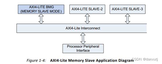
Figure1-4 shows an example application for AXI4-Lite Memory Slave Interface Type with an AXI4-Lite Interconnect to manage Control/Status Accesses. The minimum memory requirement for this configuration is set to 4K bytes. Data widths of 32 and 64 bits are supported by this configuration.
图1-4显示了一个AXI4 Lite存储器从接口类型的示例应用,该应用带有AXI4 Lite互连,用于管理控制/状态访问。此配置的最低内存要求设置为4K字节。此配置支持32位和64位的数据宽度。
(3)
读赛灵思IP手册,block memory generator Product Guide,即内存memory系列(如RAM ROM等)的手册。本期介绍AXI4 Interface Block Memory Generator Feature Summary(3)AXI4接口BMG功能概述(3)Applications。
P13
AXI4 Block Memories–Peripheral Slave Mode
AXI4 Block Memories in Peripheral Slave mode are optimized for a system or applications requiring data transfers that are grouped together in packets. The AXI4 Peripheral Slave supports aligned /unaligned addressing for incremental bursts.
AXI4块存储器–外设从属模式
外设从属模式下的AXI4块存储器针对需要分组数据传输的系统或应用进行了优化。AXI4外围从设备支持增量突发的对齐/未对齐寻址。
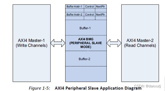
Figure 1-5 shows an example application for the AXI4 Peripheral Slave Interface Type in a Point-to-point buffered link list application. There is no minimum memory requirement set for this configuration. Data widths supported by this configuration include 8, 16, 32, 64, 128 and 256 bits.
图1-5显示了点对点缓冲链路列表应用程序中AXI4外设从接口类型的示例应用。此配置没有设置最低内存要求。此配置支持的数据宽度包括8、16、32、64、128和256位。
AXI4-Lite Block Memories–Peripheral Slave Mode
AXI4-Lite Block Memories in Peripheral Slave mode are optimized for the AXI4-Lite interface. They can be used in implementations requiring single burst transactions
AXI4 Lite块存储器–外设从属模式
AXI4 Lite块存储器在外设从属模式下针对AXI4 Lite接口进行了优化。它们可以用于需要单突发事务的实现中
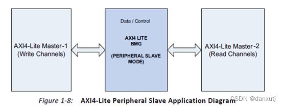
Figure 1-8 shows an example application for the AXI4-Lite Memory Slave Interface Type in a Point-to-point application. There is no minimum memory requirement set for this configuration. Data widths supported by this configuration include 8, 16, 32 and 64 bits.
图1-8显示了点对点应用中AXI4 Lite存储器从接口类型的示例应用。此配置没有设置最低内存要求。此配置支持的数据宽度包括8、16、32和64位。
(4)
读赛灵思IP手册,block memory generator Product Guide,即内存memory系列(如RAM ROM等)的手册。本期介绍AXI4 Interface Block Memory Generator Feature Summary(4)AXI4接口BMG功能概述(4)握手序列。
P14
AXI4 BMG Core Channel Handshake Sequence
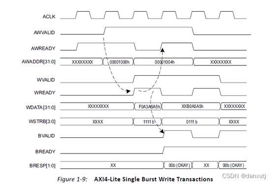
Figure 1-9 and Figure 1-10 illustrates an example handshake sequence for AXI4 BMG core. Figure 1-9 illustrates single burst Write operations to block RAM. By default the awready signal is asserted on the bus so that the address can be captured immediately during the clock cycle when both awvalid and awready are asserted. (With the default set in this manner, there is no need to wait an extra clock cycle awready to be asserted first.) By default, the wready signal is deasserted. Upon detecting awvalid being asserted, the wready signal is asserted (AXI4 BMG core has registered an AXI Address and is ready to accept Data), and when wvalid is also asserted, writes are performed to the block RAM. If the write data channel (wvalid) is presented prior to the write address channel valid (awvalid) assertion, the write transactions are not initiated until the write address channel has valid information.
AXI4 BMG核心信道握手序列
图1-9和图1-10说明了AXI4 BMG核心的示例握手序列。图1-9说明了块RAM的单脉冲串写入操作。默认情况下,awready信号在总线上被断言,因此当awvalid和awready都被断言时,可以在时钟周期内立即捕获地址。(通过这种方式设置默认值,无需等待额外的时钟周期awready才能首先被断言。)默认情况下,wrady信号被取消断言。在检测到wvalid被断言时,wready信号被断言(AXI4 BMG内核已注册AXI地址并准备好接受数据),并且当wvalid也被断言时对块RAM执行写入。如果写入数据通道(wvalid)在写入地址通道有效(awvalid)断言之前出现,则在写入地址信道具有有效信息之前不会启动写入事务。
The Block Memory Generator core with AXI4 Interface asserts bvalid for each transaction only after the last data transfer is accepted. The core also does not wait for the master to assert bready before asserting bvalid.
带有AXI4接口的块内存生成器核心仅在接受最后一次数据传输后才为每个事务声明bvalid。内核也不会在断言bvalid之前等待主控断言bredy。
Note: The signal names in the figures displayed in upper case are the same as the lower case signal names referred to in the text.
注:图中以大写显示的信号名称与文本中提及的小写信号名称相同。
P15
Figure 1-10 illustrates single burst Read operations to block RAM. The registered arready signal output on the AXI Read Address Channel interface defaults to a High assertion. The AXI Read FSM can accept the read address in the clock cycle where the arvalid signal is first valid.
图1-10说明了块RAM的单脉冲串读取操作。AXI读取地址通道接口上注册的arrady信号输出默认为High断言。AXI读取FSM可以在arvalid信号首先有效的时钟周期中接受读取地址。
The AXI Read FSM can accept a same clock cycle assertion of the rready by the master if the master can accept data immediately. When the rready signal is asserted on the AXI bus by the master, the Read FSM either negates the rvalid signal or places the next valid data on the AXI Bus.
如果主设备可以立即接受数据,AXI读取FSM可以接受主设备的相同时钟周期断言。当主控器在AXI总线上断言rready信号时,读取FSM要么否定rvalid信号,要么将下一个有效数据置于AXI总线。
For more details on AXI4 Channel handshake sequences refer to the “Channel Handshake” section of the AXI Protocol Specification [Ref 1].
有关AXI4信道握手序列的更多详细信息,请参阅AXI协议规范[参考文献1]的“信道握手”部分。
(5)
读赛灵思IP手册,block memory generator Product Guide,即内存memory系列(如RAM ROM等)的手册。本期介绍AXI4 Interface Block Memory Generator Feature Summary(5)AXI4接口BMG功能概述(5)突发事务。
P16
AXI4-Lite Single Burst Transactions
For AXI4 Lite interfaces, all transactions are burst length of one and all data accesses are the same size as the width of the data bus. Figure 1-9 and Figure 1-10 illustrates timing of AXI 32-bit write operations to the 32-bit wide block RAM. Figure 1-9 example illustrates single burst Write operations to block RAM addresses 0x1000h and 0x1004h. Figure 1-10 illustrates single burst Read operations to block RAM addresses 0x1000h and 0x1004h.
AXI4 Lite单突发事务
对于AXI4Lite接口,所有事务的突发长度为1,所有数据访问的大小与数据总线的宽度相同。图1-9和图1-10说明了AXI 32位写入32位宽块RAM操作的时序。图1-9示例说明了用于块RAM地址0x1000h和0x1004h的单脉冲串写入操作。图1-10说明了单脉冲串读取操作以阻止RAM地址0x1000h和0x1004h。
AXI4 Incremental Burst Support
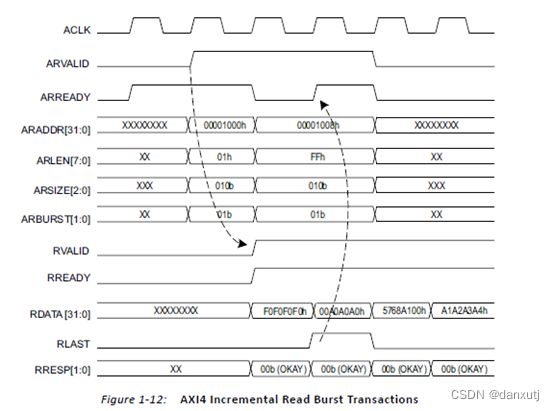
Figure 1-11 illustrates an example of the timing for an AXI Write burst of four words to a 32-bit block RAM. The address Write channel handshaking stage communicates the burst type as INCR, the burst length of two data transfers (awlen = 01h). The Write burst utilizes all byte lanes of the AXI data bus going to the block RAM (awsize = 010b).
In compliance with AXI Protocol, the burst termination boundary for a transaction is determined by the length specified in the awlen signal. The allowable burst sizes for INCR bursts are from 1 (00h) to 256 (FFh) data transfers.
AXI4增量突发支持
图1-11说明了一个32位块RAM的四个字的AXI写入脉冲串的定时示例。地址写入通道握手阶段将突发类型作为INCR进行通信,即两次数据传输的突发长度(awlen=01h)。写入脉冲串利用AXI数据总线的所有字节通道到达块RAM(awsize=010b)。
根据AXI协议,事务的突发终止边界由awlen信号中指定的长度确定。INCR突发的允许突发大小为1(00h)到256(FFh)数据传输。
Figure 1-12 illustrates the example timing for an AXI Read burst with block RAM managed by the Read FSM. The memory Read burst starts at address 0x1000h of the block RAM. On the AXI Read Data Channel, the Read FSM enables the AXI master/Interconnect to respond to the rvalid assertion when rready is asserted in the same clock cycle. If the requesting AXI master/Interconnect throttles on accepting the Read burst data (by negating rready), the Read FSM handles this by holding the data pipeline until rready is asserted.
图1-12说明了由读取FSM管理的具有块RAM的AXI读取突发的示例时序。存储器读取脉冲串从块RAM的地址0x1000h开始。在AXI读取数据通道上,读取FSM使AXI主控器/互连器能够在同一时钟周期内断言就绪时响应rvalid断言。如果请求的AXI主控/互连在接受读突发数据时(通过否定rready)节流,则读FSM通过保持数据管道直到断言rready来处理此问题。
(6)
读赛灵思IP手册,block memory generator Product Guide,即内存memory系列(如RAM ROM等)的手册。本期介绍AXI4 Interface Block Memory Generator Feature Summary(6)AXI4接口BMG功能概述(6)AXI4包突发支持。
P18
AXI4 Wrap Burst Support
Cache line operations are implemented as WRAP burst types on AXI when presented to the block RAM. The allowable burst sizes for WRAP bursts are 2, 4, 8, and 16. The awburst/arburst must be set to 10 for the WRAP burst type.
AXI4包突发支持
当呈现给block RAM时,缓存线操作在AXI上实现为WRAP突发类型。WRAP突发的允许突发大小为2、4、8和16。对于WRAP突发类型,awburst/abrurst必须设置为10。
WRAP bursts are handled by the address generator logic of the Write and Read FSM. The address seen by the block RAM must increment to the address space boundary, and then wrap back around to the beginning of the cache line address. For example, a processor issues a target word first cache line Read request to address 0x04h. On a 32-bit block RAM, the address space boundary is 0xFFh. This means that the block RAM sees the following sequence of addresses for Read requests: 0x04h, 0x08h, 0x0Ch, 0x00h. Note the wrap of the cache line address from 0xCh back to 0x00h at the end.
WRAP突发由写和读FSM的地址生成器逻辑处理。Block RAM看到的地址必须增加到地址空间边界,然后返回到缓存行地址的开头。例如,处理器向地址0x04h发出目标字第一缓存行读取请求。在32位block RAM上,地址空间边界为0xFFh。这意味着块RAM看到以下读取请求的地址序列:0x04h、0x08h、0x0Ch、0x00h。注意缓存行地址从0xCh返回到结尾的0x00h。
图片
Figure 1-13 illustrates the timing for AXI Wrap or cache line burst transactions. The address generated and presented to the block RAM starts at the target word and wraps around after the address space boundary is reached.
Figure 1-14 illustrates the timing on AXI WRAP or cache line burst Read transactions.
图1-13说明了AXIWrap或缓存线突发事务的时序。生成并呈现给block RAM的地址从目标字开始,并在到达地址空间边界后环绕。
图1-14说明了AXIWRAP或缓存线突发读取事务的时序。
Table 1-4 provides example address sequence to the block RAM for Wrap transactions.
Notes:
- Calculated Wrap Boundary address
笔记:
1.计算的包裹边界地址
For more details on AXI4 Wrap Burst Transactions and Wrap boundary calculations, refer to the Burst Addressing section of the AXI Protocol Specification [Ref 1].
有关AXI4包裹突发事务和包裹边界计算的更多详细信息,请参阅AXI协议规范[参考文献1]的突发寻址部分。
(7)
读赛灵思IP手册,block memory generator Product Guide,即内存memory系列(如RAM ROM等)的手册。本期介绍AXI4 Interface Block Memory Generator Feature Summary(7)AXI4接口BMG功能概述(7)AXI4窄事务。
P21
AXI4 Narrow Transactions
A narrow burst is defined as a master bursting a data size smaller than the block RAM data width. If the burst type (awburst) is set to incr or wrap, then the valid data on the block RAM interface to the AXI bus rotates for each data beat. The Write and Read FSM handles each data beat on the AXI as a corresponding data beat to the block RAM, regardless of the smaller valid byte lanes. In this scenario, the AXI wsrtb is translated to the block RAM Write enable signals. The block RAM address only increments when the full address (data) width boundary is met with the narrow Write to block RAM.
Figure 1-15 illustrates an example of AXI narrow Write bursting with a 32-bit block RAM and the AXI master request is a half-word burst of four data beats. awsize is set to 001b.
AXI4窄事务
窄突发被定义为数据大小小于block RAM数据宽度的主突发。如果突发类型(awburst)被设置为incr或wrap,那么AXI总线的block RAM接口上的有效数据将针对每个数据节拍进行旋转。写和读FSM将AXI上的每个数据节拍作为block RAM的对应数据节拍进行处理,而不管有效字节通道是否较小。在这种情况下,AXI-wsrtb被转换为block RAM写入启用信号。block RAM地址仅在全地址(数据)宽度边界与窄的写入block RAM一致时递增。
图1-15显示了一个使用32位block RAM的AXI窄写突发的示例,AXI主请求是四个数据节拍的半字突发。awsize设置为001b。
Figure 1-16 illustrates an example of AXI “narrow” Read bursting with a 32-bit block RAM and the AXI master request is a half-word burst of 4 data beats. ARSIZE is set to 001b.
图1-16显示了一个带有32位块RAM的AXI“窄”读突发的示例,AXI主请求是4个数据节拍的半字突发。ARSIZE设置为001b。
For more details on AXI4 Narrow Transactions refer to the “Narrow transfers” section of the AXI Protocol Specification [Ref 1].
有关AXI4窄事务的更多详细信息,请参阅AXI协议规范[参考文献1]的“窄传输”部分。
(8)
读赛灵思IP手册,block memory generator Product Guide,即内存memory系列(如RAM ROM等)的手册。本期介绍AXI4 Interface Block Memory Generator Feature Summary(8)AXI4接口BMG功能概述(8)AXI4 Unaligned Transactions、AXI4 Interface Block Memory Addressing。
P22
AXI4 Unaligned Transactions
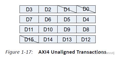
Unaligned burst transfers occur when a 32-bit word burst size does not start on an address boundary that matches a word memory location. The starting memory address is permitted to be something other than 0x0h, 0x4h, 0x8h, etc. The example shown in Figure 1-17 illustrates an unaligned word burst transaction of 4 data beats, starting at address offset, 0x1002h.
AXI4未对齐事务
当32位字突发大小未在与字存储器位置匹配的地址边界上开始时,会发生未对齐的突发传输。起始内存地址可以是0x0h、0x4h、0x8h等以外的值。图1-17所示的示例说明了从地址偏移0x1002h开始的4个数据节拍的未对齐字突发事务。
For more details on AXI4 Narrow Transactions refer to the “about unaligned transfers” section of the AXI Protocol Specification [Ref 1].
有关AXI4窄事务的更多详细信息,请参阅AXI协议规范[参考文献1]的“关于未对齐传输”部分。
Configurable Width and Depth
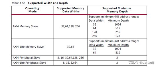
Table 1-5 provides supported width and depth for the Block Memory Generator core with AXI4 Interface.
可配置的宽度和深度
表1-5提供了带AXI4接口的块内存生成器内核的支持宽度和深度。
For Peripheral Slave configurations, there is no minimum requirement for the number of address bits used by Block Memory core. For Memory Slave configuration, AXI4 Block Memory slave has at least sufficient address bits to fully decode a 4kB address range.
对于外围从属配置,对块存储器核心使用的地址位数没有最低要求。对于存储器从属配置,AXI4块存储器从属至少有足够的地址位来完全解码4kB地址范围。
For Peripheral Slave and AXI4-Lite Memory Slave configurations, the Block Memory Generator core with AXI4 Interface is not required to have low-order address bits to support decoding within the width of the system data bus and assumes that such low-order address bits have a default value of all zeros. For AXI4 Memory Slave configuration, the Block Memory Generator core with AXI4 Interface supports Narrow Transactions and performs low-order address bits decoding. For more details, see AXI4 Interface Block Memory Addressing.
对于外设从机和AXI4 Lite存储器从机配置,具有AXI4接口的块存储器生成器内核不需要具有低阶地址位,以支持在系统数据总线宽度内的解码,并假设这种低阶地址比特具有全零的默认值。对于AXI4内存从配置,具有AXI4接口的块内存生成器内核支持窄事务并执行低阶地址位解码。有关详细信息,请参阅AXI4接口块内存寻址。
AXI4 Interface Block Memory Addressing
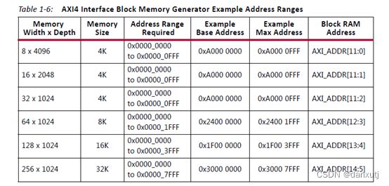
AXI4 Interface Block Memory cores support 32-bit byte addressing. There is no minimum requirement for the number of address bits supplied by a master. Typically a master is expected to supply 32-bits of addressing. Table 1-6 illustrates some example settings to create a specific size of block RAM in the system.
AXI4接口块内存寻址
AXI4接口块内存内核支持32位字节寻址。对于主机提供的地址比特数没有最低要求。通常,主设备需要提供32位寻址。表1-6说明了在系统中创建特定大小的块RAM的一些示例设置。
The Address Range of AXI Block Memory core must always start at zero. If the master has a different address bus width than that provided by the Block Memory Generator core with AXI4 interface, follow these guidelines:
• If the Master address is wider than the configured Address Range for AXI Block Memory core, the additional high-order address bits can be connected as is. AXI Block Memory core ignores these bits.
• If the Master address is narrower than 32-bits, the high-order address bits of the AXI Block Memory core can be left unconnected.
AXI块内存核心的地址范围必须始终从零开始。如果主机的地址总线宽度不同于具有AXI4接口的块内存生成器内核提供的地址总线,请遵循以下指南:
•如果主地址大于AXI块内存核心的配置地址范围,则可以按原样连接额外的高阶地址位。AXI块存储器核心忽略这些位。
•如果主地址小于32位,AXI块存储器核心的高阶地址位可以保持不连接。
For more details on AXI4 Addressing refer to the “Master Addresses” and “Slave Addresses” section of the AXI Protocol Specification [Ref 1].
有关AXI4寻址的更多详细信息,请参阅AXI协议规范[参考文献1]的“主地址”和“从地址”部分。


