PCIe Spec View (一)
环境
- PCI Express Technology-Comprehensive Guide to Generations 1.x, 2.x, 3.0
- PCI Express 体系结构导读
1 PCIe 基本概念
- Link: A physical connection between two PCIe devices is called, a Link and is made up of one or more Lanes.
- PCIe uses dual‐simplex(双单工模式) connection that each lane has a simplex(单一的) transmit path and a simplex receive path.
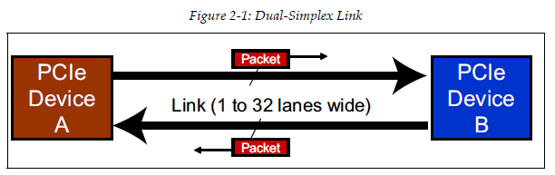
- Lane: One such pair is called a Lane, and the spec allows a Link to be made up 1, 2, 4, 8, 12, 16, or 32 Lanes. The number of lanes is called the Link Width and is represented as x1, x2, x4, x8, x16, and x32.

1.2 PCIe 速度

- Gen1 PCIe Bandwidth = ( (2.5 GT/s x 2 (双向通道)) x (8/10) ) / 8 bits per symbol = 0.5GB/s.
- Gen2 PCIe Bandwidth = ( (5.0 GT/s x 2 (双向通道)) x (8/10) ) / 8 bits per symbol = 1.0GB/s.
- Gen3 PCIe Bandwidth = ( (8.0 GT/s x 2 (双向通道)) x (128/130) ) / 8 bits per symbol ≈ 2GB/s.
T/s是每秒传输数量(Transfer per second),有效带宽要结合传输协议来计算.T/s可以看成是未经过编码的原始数据.- PCIe 1.0 单向通道
2.5GT/s,8b/10b编码(每次传输10bit,其中8bit是数据,2bit校验位),有效带宽为2Gbps. - PCIe 2.0 单向通道
5 GT/s,8b/10b编码(每次传输10bit,其中8bit是数据,2bit校验位),有效带宽为4Gbps. - PCIe 3.0 单向通道
8 GT/s,128b/130b编码(每次传输130bit,其中128bit是数据,2bit校验位),有效带宽约为8Gbps.
1.3 Packet-based Protocol
- PCIe reduces pin count by eliminating most side‐band control signals.
- How can the receiver interpret the incoming bits if there are no control signals indicating the type of information being received? All transactions in PCIe are sent in defined structures called packets.
- The receiver finds the packet boundaries and, knowing the pattern to expect, decodes the packet structure to determine what it should do.
1.4 PCIe拓扑结构
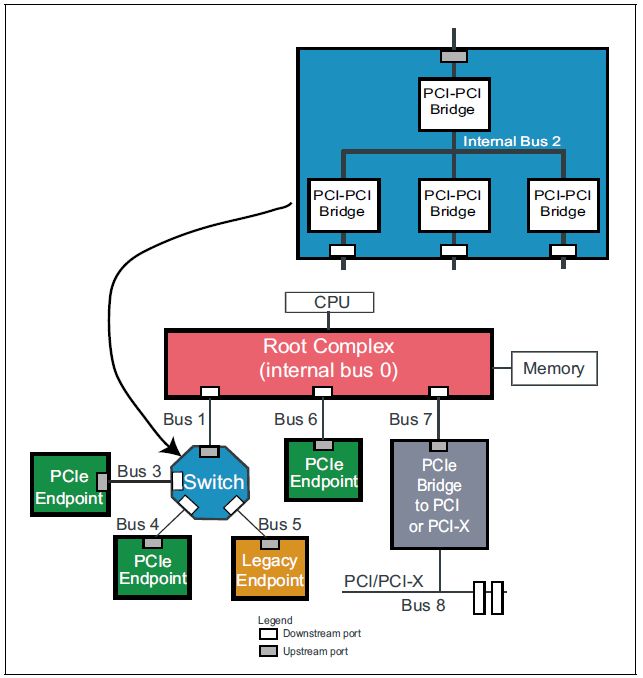
- PCIe拓扑结构是一个树形结构.
- 主要包括Root Complex, Switch, PCIe Bridge.
1.4.1 Root Complex
- Root Complex(RC)是树的根,它为CPU代言,与整个计算机系统其他部分通信,比如CPU通过它访问内存,通过它访问PCIe系统中的设备.
- Root Complex: A Root Complex (RC) denotes the root of an I/O hierarchy that connects the CPU/memory subsystem to the I/O.
1.4.2 Switch
- Switch由一个上游端口(Upstream Port)和2~n个下游端口(Downstream Port)组成.
- Switch的作用就是扩展PCIe端口,并为挂在它上面的设备(Endpoint或者Switch)提供路由和转发服务.
- 每个Switch内部,也是有一根内部PCIe总线的,然后通过若干个Bridge,扩展出若干个下游端口
- 从系统配置软件看,Switch内部由多个虚拟PCI-to-PCI桥组成. Switch内部上游和下游端口都对应一个PCI-to-PCI桥,每个桥都有PCI配置空间. 在Switch内部还有一条虚拟的PCI总线,用来连接每个虚拟PCI桥.
- To configuration software, a Switch appears as a collection of virtual PCI-to-PCI Bridges.
- Switches: A Switch is defined as a logical assembly of multiple virtual PCI-to-PCI Bridge devices. A Switch may have several Downstream Ports but can only have one Upstream Port. Switches provide a fanout or aggregation capability and allow more devices to be attached to a single PCIe Port. They act as packet routers and recognize which path a given packet will need to take based on its address or other routing
information.
1.4.3 Bridge
- Bridge provides an interface to other buses, such as PCI or PCI‐X, or even another PCIe bus.
- Bridge is a function that virtually or actually connects a PCI/PCI-X segment or PCI Express Port with an internal component interconnect or with another PCI/PCI-X bus segment or PCI Express Port.
- PCIe bridge 可以将PCIe总线转换成PCI总线,用于连接PCI设备。
- PCIe bridge 可以将PCI总线转换成PCIe总线(Reverse Bridge),用于连接PCIe设备。
1.4.4 Endpoint
- Endpoints: Endpoints are devices in a PCIe topology that are not Switches or bridges and act as initiators or Completers of transactions on the bus. They reside at the bottom of the branches of the tree topology and only implement a single Upstream Port (facing toward the Root).
- Endpoint refers to a type of Function that can be the Requester or Completer of a PCI Express transaction either on its own behalf or on behalf of a distinct non-PCI Express device.
1.4.5 PCIe Buses
-
Up to
256Bus Numbers can be assigned by configuration software. The initial Bus Number, Bus 0, is typically assigned by hardware to the Root Complex. Bus 0 consists of a Virtual PCI bus with integrated endpoints and Virtual PCI‐to‐PCI Bridges (P2P) which are hard‐coded with a Device number and Function number. -
Configuration software begins the process of assigning bus numbers by searching for bridges starting with Bus 0, Device 0, Function 0. When a bridge is found, software(depth first search) assigns the new bus a bus number that is unique and larger than the bus number the bridge lives on.
1.4.6 PCIe Devices
- PCIe permits up to
32device attachments on a single PCI bus, however, the point‐to‐point nature of PCIe means only a single device can be attached directly to a PCIe link and that device will always end up being Device 0.
1.4.7 PCIe functions
- PCIe contains up to
8functions that all share the bus interface for that device, numbered 0‐7.Devices that have multiple Functions do not need to be implemented sequentially.
TODO
- TODO 1:
what's difference between Switch and Bridge?
PCIe Switch和Bridge是用于PCIe技术的两种不同类型的设备,它们之间有以下几个不同之处:
- 功能:PCIe Switch是一个多端口设备,可以连接多个PCIe设备,并提供高速数据传输和路由功能。它允许多个设备同时进行通信,并提供更高的带宽和吞吐量。
- 数据转发:PCIe Switch可以根据目标设备的地址将数据包转发到正确的端口,从而实现设备之间的直接通信。而PCIe Bridge则只能将数据包从一个PCIe总线传递到另一个PCIe总线,起到桥接的作用。
- 扩展性:由于PCIe Switch具有多个端口,它通常用于大型系统或数据中心,可以连接多个设备。而PCIe Bridge通常用于较小的系统或单板计算机,只需要连接两个PCIe总线。
- 性能:PCIe Switch通常具有更高的带宽和更快的数据传输速度,因为它们专为高速PCIe总线设计。PCIe Bridge的性能相对较低,适用于较小规模的数据传输。
总而言之,PCIe Switch是一个多端口设备,具有高速数据传输和路由功能,用于连接多个PCIe设备,而PCIe Bridge是一个桥接设备,用于连接两个PCIe总线,功能相对较简单。
- TODO 2:
what's the virtual PCI bus?
Virtual PCI bus refers to a virtualized representation of a PCI bus within a virtualization environment. In virtualization, a physical server is divided into multiple virtual machines (VMs), each running its own operating system. These VMs may require access to PCI devices for various purposes, such as network adapters or storage controllers.
To provide virtual machines with access to PCI devices, a virtual PCI bus is created within the virtualization software. This virtual bus acts as an intermediary between the physical PCI bus on the host machine and the virtual machines. It allows the virtual machines to communicate with and utilize the PCI devices as if they were directly connected to their own dedicated PCI bus.
The virtual PCI bus facilitates the sharing and allocation of physical PCI devices among multiple virtual machines. It enables efficient utilization of hardware resources and allows for the consolidation of multiple systems onto a single physical server. Virtualization technologies like VMware, Hyper-V, and KVM provide mechanisms to create and manage virtual PCI buses within their virtualization platforms.
2 PCIe Configuration
why we need PCIe configuration?
Each PCIe device should have a Configuration space that was acquired for Host software to get device information and to configure the device.
2.1 Configuration Address Space
- PCI defines a dedicated block of configuration address space for each Function.
2.1.1 PCI-Compatible Space
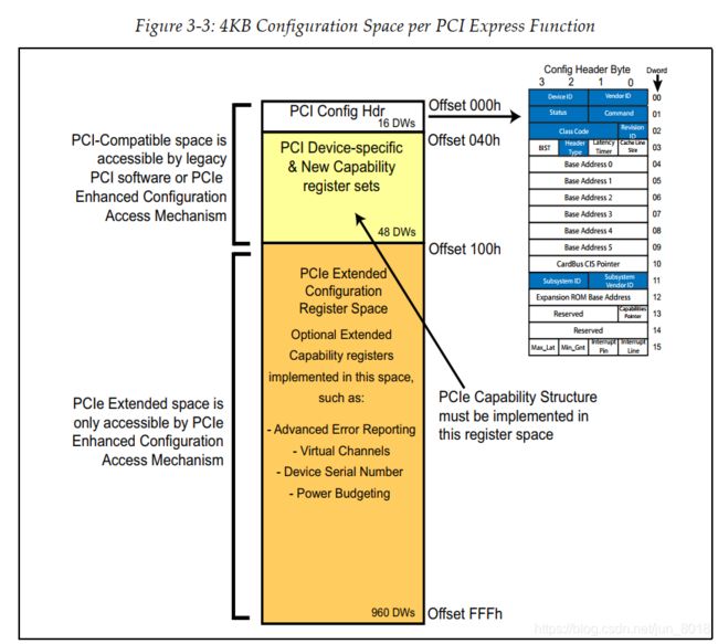
- The 256 bytes of PCI‐compatible configuration space was so named because it was originally designed for PCI.
- The first 16 dwords (64 bytes) of this space are the configuration header (Header Type 0(for functions ) or Header Type 1(for bridges)) .
- The remaining 48 dwords(192 bytes) are used for optional registers including PCI capability structures.

2.1.2 PCIe Extended Configuration Space
- When PCIe was introduced, there was not enough room in the original 256‐byte configuration region to contain all the new capability structures needed. So the size of configuration space was expanded from 256 bytes per function to 4KB(960 dwords).
- The 960 dwords(4KB) Extended Configuration area is only accessible using the Enhanced configuration mechanism and is therefore not visible to legacy PCI software.
- PCIe Functions must implement the following Capability Structures: (1)PCI Express Capability; (2)Power Management; (3)MSI and/or MSI‐X
2.2 Access Configuration
Only the Root Sends Configuration Requests. why?- (1) The ability to originate configuration transactions is restricted to the processor through the Root Complex to avoid the anarchy(chaos)that could result if any device had the ability to change the configuration of other devices.
- (2) Processors are generally unable to perform configuration read and write requests directly because they can only generate memory and IO requests.
- From the above two reason, we can conclude that Root Complex will need to translate certain of those accesses(memory and IO requests) into configuration requests in support of this process.
- Configuration space can be accessed using either of two mechanisms:
• Thelegacy PCI configuration mechanism,using IO‐Indirect accesses.
• Theenhanced configuration mechanism, using memory‐mapped accesses.
2.2.1 Legacy PCI configuration mechanism
- The
legacy PCI configuration mechanism,using IO‐Indirect accesses. - The Legacy PCI (PCI‐Compatible) mechanism uses two 32‐bit IO ports in the Host bridge of the Root Complex. They are the
Configuration Address Port, at IO addresses0CF8h ‐ 0CFBh, and theConfiguration Data Port,at IO addresses0CFCh ‐CFFh. - The
Configuration Address Portonly latches information when the processor performs a full 32‐bit write to the port and a 32‐bit read from the port returns its contents. - The information written to the Configuration Address Port must conform to the following template.

Bit [31]must be set to1bto enable translation of the subsequent IO access to the Configuration Data Port into a configuration access. If bit 31 is zero and an IO read or write is sent to the Configuration Data Port, the transaction is treated as anordinary IO Request.- Example PCI-Compatible Configuration Acces
mov dx,0CF8h 		;set dx = config address port address
mov eax,80040000h	;enable=1, bus 4, dev 0, func 0, DW 0
out dx,eax       	;IO write to set up address port
mov dx,0CFCh 		;set dx = config data port address
in ax,dx     		;2-byte read from config data port
2.2.1.1 Bus Compare and Data Port Usage
- The Host Bridge within the Root Complex implements a Secondary Bus Number(sBusnum) register and a Subordinate Bus Number(subBusnum) register.
- The Secondary Bus Number is the bus number of the bus immediately beneath the bridge.
- The Subordinate Bus Number is the target bus number that lives downstream of the bridge.
2.2.1.1.1 BUS Compare
When a Request is seen, the Bridge evaluates whether the target bus number(tgrtBusnum) is within the range of bus numbers downstream, from the value of the Secondary Bus number to the Subordinate Bus number.
if (tgrtBusnum == sBusnum)
    targeted the bus and the Request is passed through as a Type 0 Configuration Request
else if((trgtBusnum > sBusnum)&&(trgtBusnum<=subBusnum))
    The Request will be forwarded as a Type1 configuration request on the bridge’s secondary bus.
- Only Bridge devices pay attention to Type 1 configuration Requests.
2.2.1.1.2 Data port usage
- If bit 31 is
1band the target bus is within the downstream range of bus numbers, the bridge translates a subsequent processor access targeting its Configuration Data Port into a configuration request on bus 0. - The processor then initiates an IO read or write transaction to the Configuration Data Port at 0CFCh.
- This causes the bridge to generate a Configuration Request that is a read when the IO access to the Configuration Data Port was a read, or a Configuration write if the IO access was a write.
2.2.2 Enhanced Configuration Access
-
The
enhanced configuration mechanism, using memory‐mapped accesses. -
Rather than try to conserve address space, they would create a single step, uninterruptable process by mapping all of configuration space into memory addresses.
-
Mapping 4KBper Function for all the possible implementations requires allocating256MB(256 * 32 * 8 * 4KB ) of memory address space. -
To handle this mapping, each Function’s 4KB configuration space starts at a 4KB‐aligned address within the 256MB memory address space set aside for configuration access, and the address bits now carry the identifying information about which Function is targeted.

-
Example Enhanced Configuration Access
mov ax,[E0400000h] 		;memory-mapped Config read

• Address bits 63:28 indicate the upper 36 bits of the 256MB‐aligned base address of the overall Enhanced Configuration address range (in this case, 00000000 E0000000h).
• Address bits 27:20 select the target bus (in this case, 4).
• Address bits 19:15 select the target device (in this case, 0) on the bus.
• Address bits 14:12 select the target Function (in this case, 0) within the device.
• Address bits 11:2 selects the target dword (in this case, 0) within the selected Function’s configuration space.
• Address bits 1:0 define the start byte location within the selected dword (in this case, 0).
2.3 Configuration Requests
- Two request types,
Type 0 or Type 1, may be generated by bridges in response to a configuration access.
2.3.1 Type 0 Configuration Request
if (trgtBusnum == sBusnum){
    if(trgtDevnum == Devnum){
        if(trgtFuncnum == Funcnum){
            use the target request register filed to select the target dword in its configuration space, and uses the First Dword Byte Enable field to select which bytes to read or write within the selected dword.
        }
    }
}

- In both read and write configuration cases, the Type field = 00100, while the Fmt field indicates whether it’s a read or a write.
2.3.2 Type 1 Configuration Request
- When a bridge sees a configuration access whose target bus number does not match its Secondary Bus Number but is in the range between its Secondary and Subordinate Bus Numbers, it forwards the packet as a Type 1 Request to its Secondary Bus.
- Devices that are not bridges (Endpoints) know to
ignore Type 1 Requestssince the target resides on a different bus, but bridges that see it will make the same comparison of the target bus number to the range of buses downstream.
if (trgtBusnum == sBusnum){
    if(trgtDevnum == Devnum){
        if(trgtFuncnum == Funcnum){
            use the target request register filed to select the target dword in its configuration space, and uses the First Dword Byte Enable field to select which bytes to read or write within the selected dword.
        }
    }
}
else if((trgtBusnum > sBusnum)&&(trgtBusnum<=subBusnum))
    The Request will be forwarded as a Type1 configuration request on the bridge’s           secondary bus.
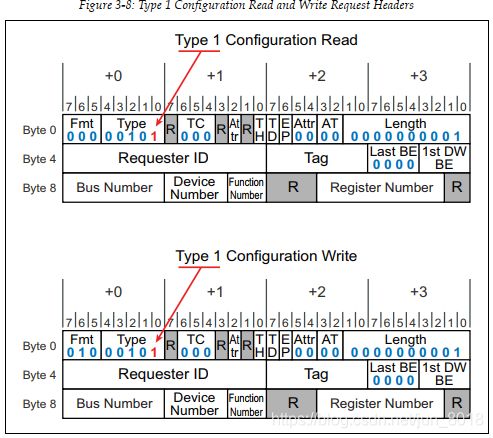
- In both cases, the Type field = 00101, while the Fmt field indicates whether it’s a read or a write.
2.4 Enumeration-Discovering the Topology
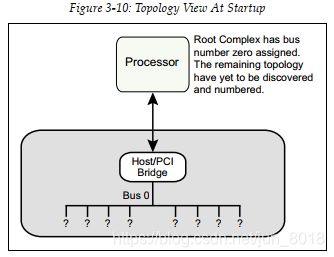
- After a system reset or power up, configuration software has to scan the PCIe fabric to discover the machine topology and learn how the fabric is populated.
- The only thing that software can know for sure is that there will be a
Host/PCI bridgeand thatbus number 0will be on the secondary side of that bridge.
2.4.1 Discovering the Presence or Absence of a Function
- The configuration software executing on the processor normally discovers the existence of a Function by reading from its Vendor ID register.
- For PCI, the Configuration Read request to a non‐existent device will return vendor ID
FFFFh. If enumeration software saw that result for the read, it understood that the device wasn’t present. - For PCIe, a Configuration Read Request to a non‐existent device will result in the bridge above the target device returning a Completion without data that has a status of UR (Unsupported Request).
- For backward compatibility with the legacy enumeration model, the Root Complex returns all ones (
FFFFh) to the processor for the data when this Completion is seen during enumeration.
2.4.2 Device not Ready
- Another problem that can arise is that the targeted device is present but isn’t ready to respond to a configuration access.
if(datRate <= 5.0GT/s)
   Configuration software wait 100ms after reset before sending a Configuration request
else if(datRate > 5.0GT/s)
   Configuration software wait 100ms after Link training completes before sending request
2.4.3 Determining if a Function is an Endpoint or Bridge
- The lower
7 bits(6:0)of the Header Type register (offset 0Eh in configure space header) identify the basic category of the Function, and three values are defined:
• 0 = not a bridge (Endpoint in PCIe)
• 1 = PCI‐to‐PCI bridge (abbreviated as P2P) connecting two buses
• 2 = CardBus bridge (legacy interface not often used today)
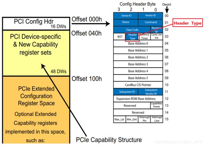

- The
bit7of the Header Type register shows whether the device consists single function(0) or multi function(1).
2.4.4 Enumeration process example(Single Root Enumeration)

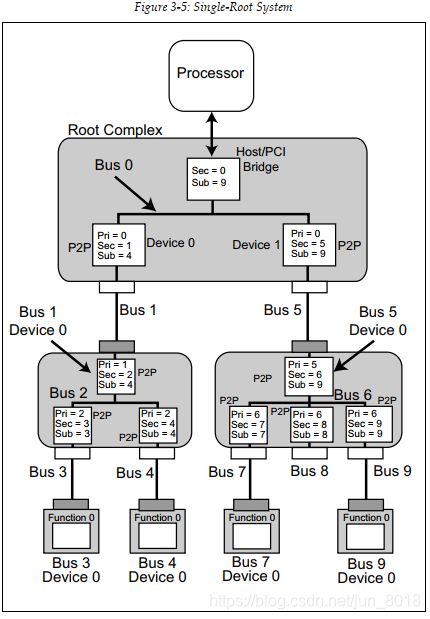
Figure 3‐13(above picture) illustrates an example system after the buses and devices have been enumerated.
1. Software updates the Host/PCI bridge Secondary Bus Number to zero and
the Subordinate Bus Number to 255. Setting this to the max value means
that it won’t have to be changed again until all the bus numbers downstream
have been identified. For the moment, buses 0 through 255 are identified
as being downstream.
2. Starting with Device 0 (bridge A), the enumeration software attempts to
read the Vendor ID from Function 0 in each of the 32 possible devices on
bus 0. If a valid Vendor ID is returned from Bus 0, Device 0, Function 0, the
device exists and contains at least one Function. If not, go on to probe bus 0,
device 1, Function 0.
3. The Header Type field in this example (Figure 3‐12 on page 108) contains
the value one (01h) indicating this is a PCI‐to‐PCI bridge. The Multifunction
bit (bit 7) in the Header Type register is 0, indicating that Function 0 is the
only Function in this bridge. The spec doesn’t preclude implementing multiple
Functions within this Device and each of these Functions, in turn, could represent
other virtual PCI‐to‐PCI bridges or even non‐bridge functions.
4. Now that software has found a bridge, performs a series of configuration
writes to set the bridge’s bus number registers as follows:
• Primary Bus Number Register = 0
• Secondary Bus Number Register = 1
• Subordinate Bus Number Register = 255
The bridge is now aware that the number of the bus directly attached
downstream is 1 (Secondary Bus Number = 1) and that the largest bus number
downstream of it is 255 (Subordinate Bus Number = 255).
5. Enumeration software must perform a depth‐first search. Before proceeding
to discover additional Devices/Functions on bus 0, it must proceed to
search bus 1.
6. Software reads the Vendor ID of Bus 1, Device 0, Function 0, which targets
bridge C in our example. A valid Vendor ID is returned, indicating that
Device 0, Function 0 exists on Bus 1.
7. The Header Type field in the Header register contains the value one
(0000001b) indicating another PCI‐to‐PCI bridge. As before, bit 7 is a 0, indicating that bridge C is a single‐function device.
8. Software now performs a series of configuration writes to set bridge C’s bus
number registers as follows:
• Primary Bus Number Register = 1
• Secondary Bus Number Register = 2
• Subordinate Bus Number Register = 255
9. Continuing the depth‐first search, a read is performed from bus 2, device 0,
Function 0’s Vendor ID register. The example assumes that bridge D is
Device 0, Function 0 on Bus 2.
10. A valid Vendor ID is returned, indicating bus 2, device 0, Function 0 exists.
11. The Header Type field in the Header register contains the value one
(0000001b) indicating that this is a PCI‐to‐PCI bridge, and bit 7 is a 0, indicating
that bridge D is a single‐function device.
12. Software now performs a series of configuration writes to set bridge D’s bus
number registers as follows:
• Primary Bus Number Register = 2
• Secondary Bus Number Register = 3
• Subordinate Bus Number Register = 255
13. Continuing the depth‐first search, a read is performed from bus 3, device 0,
Function 0’s Vendor ID register.
14. A valid Vendor ID is returned, indicating bus 3, device 0, Function 0 exists.
15. The Header Type field in the Header register contains the value zero
(0000000b) indicating that this is an Endpoint function. Since this is an endpoint
and not a bridge, it has a Type 0 header and there are no PCI‐compatible
buses beneath it. This time, bit 7 is a 1, indicating that this is a
multifunction device.
16. Enumeration software performs accesses to the Vendor ID of all 8 possible
functions in bus 3, device 0 and determines that only Function 1 exists in
addition to Function 0. Function 1 is also an Endpoint (Type 0 header), so
there are no additional buses beneath this device.
17. Enumeration software continues scanning across on bus 3 to look for valid
functions on devices 1 ‐ 31 but does not find any additional functions.
18. Having found every function there was to find downstream of bridge D,
enumeration software updates bridge D, with the real Subordinate Bus
Number of 3. Then it backs up one level (to bus 2) and continues scanning
across on that bus looking for valid functions. The example assumes that
bridge E is device 1, Function 0 on bus 2.
19. A valid Vendor ID is returned, indicating that this Function exists.
20. The Header Type field in bridge E’s Header register contains the value one
(0000001b) indicating that this is a PCI‐to‐PCI bridge, and bit 7 is a 0, indicating a single‐function device.
21. Software now performs a series of configuration writes to set bridge E’s bus
number registers as follows:
• Primary Bus Number Register = 2
• Secondary Bus Number Register = 4
• Subordinate Bus Number Register = 255
22. Continuing the depth‐first search, a read is performed from bus 4, device 0,
Function 0’s Vendor ID register.
23. A valid Vendor ID is returned, indicating that this Function exists.
24. The Header Type field in the Header register contains the value zero
(0000000b) indicating that this is an Endpoint device, and bit 7 is a 0, indicating that this is a single‐function device.
25. Enumeration software scans bus 4 to look for valid functions on devices 1 ‐
31 but does not find any additional functions.
26. Having reached the bottom of this tree branch, enumeration software
updates the bridge above that bus, E in this case, with the real Subordinate
Bus Number of 4. It then backs up one level (to bus 2) and moves on to read
the Vendor ID of the next device (device 2). The example assumes that
devices 2 ‐ 31 are not implemented on bus 2, so no additional devices are
discovered on bus 2.
27. Enumeration software updates the bridge above bus 2, C in this case, with
the real Subordinate Bus Number of 4 and backs up to the previous bus
(bus 1) and attempts to read the Vendor ID of the next device (device 1). The
example assumes that devices 1 ‐ 31 are not implemented on bus 1, so no
additional devices are discovered on bus 1.
28. Enumeration software updates the bridge above bus 1, A in this case, with
the real subordinate Bus Number of 4. and backs up to the previous bus
(bus 0) and moves on to read the Vendor ID of the next device (device 1).
2.4.5 Enumeration process example(Multi-Root Enumeration)
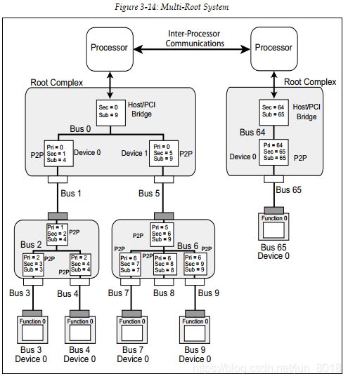
During enumeration of the left‐hand tree structure in Figure 3‐14 on page 116,
the Host/PCI bridge in the secondary Root Complex ignores all configuration
accesses because the targeted bus number is no greater than 9. Note that,
although detected and numbered, Bus 8 has no device attached. Once that enumeration process has been completed, the enumeration software takes the following steps to enumerate the secondary Root Complex:
1. The enumeration software changes the Secondary and Subordinate Bus
Number values in the secondary Root Complex’s Host/PCI bridge to bus 64
in this example. (The values of 64 and 128 are commonly used as the starting
bus number in multi‐root systems, but this is just a software convention.
There are no PCI or PCIe rules requiring that configuration. There would be
nothing wrong with starting the secondary Root Complex’s bus numbers at 10 in this example.)
2. Enumeration software then starts searching on bus 64 and discovers the
bridge attached to the downstream Root Port.
3. A series of configuration writes are performed to set its bus number registers
as follows:
• Primary Bus Number Register = 64
• Secondary Bus Number Register = 65
• Subordinate Bus Number Register = 255
The bridge is now aware that the number of the bus directly attached to its
downstream side is 65 (Secondary Bus Number = 65) and the number of the
bus farthest downstream of it is 65 (Subordinate Bus Number = 65).
4. Device 0 is discovered on Bus 65 that implements a only Function 0, and
further searching reveals no other Devices are present on Bus 65, so the
search process moves back up one Bus level.
5. Enumeration continues on bus 64 and no additional devices are discovered,
so the Host/PCI’s Subordinate Bus Number is updated to 65.
6. This completes the enumeration process.
2.5 Useful software Tool
MindShare Arbor is a computer system debug, validation, analysis and learning tool that allows the user to read and write any memory, IO or configuration space address. It maybe need money :–(.
3 Address Space and Transaction Routing
- Almost all devices have internal registers or storage locations that software need to be able to access. This means these internal registers or locations need to be addressable.
- These internal registers or locations need to be assigned addresses from one of the
address spacessupported in the system. - PCI Express supports the exact same three
address spacesthat were supported in PCI:
• Configuration address space
• Memory address space
• IO address space
3.1 Configuration Address Space
- please refer to
"2.1 chapter" - It is very common for PCIe devices to have device‐specific registers mapped into their config space.
- The device‐specific registers mapped into config space are often
control, status or pointer registers.
3.2 Memory Address Space and IO Address Space
- This resulted in the internal registers/storage of IO devices being mapped into memory address space (memory mapped IO, or MMIO).
- However, because early software was written to use IO address space to access internal registers/storage on IO devices, it became common practice to map the same set of device‐specific registers in memory address space as well as in IO address space.
- This allows new software to access the internal locations of a device using
memory address space (MMIO), while allowing legacy software to access the internal registers of devices usingIO address space.
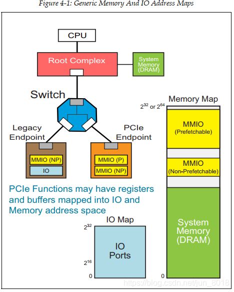
- The size of the IO map in PCIe is limited to 32 bits (4GB), although in many computers using Intel‐compatible(x86) processors, only the lower 16 bits (64KB) are used.
- PCIe can support memory addresses up to 64 bits in size.
3.2.1 P‐MMIO and NP‐MMIO
- Prefetchable MMIO (P‐MMIO) and Non‐Prefetchable MMIO (NP‐MMIO)
- Prefetchable space has two very well defined attributes:
• Reads do not have side effects
• Write merging is allowed
3.2.2 Base Address Registers(BARs)
- The system software(i.e. BIOS and OS kernel) is responsible to arrange the address of PCI‐based devices.
- The devices must provide a way for system software to determine the address space needs of the device.
- Once system software knows what the device’s requirements are in terms of address space, then if the request can be fulfilled, system software will simply allocate an available range of addresses, of the appropriate type
(IO, NP‐MMIO or P‐MMIO)to that device.
- This is all accomplished through the Base Address Registers (BARs) in the header of configuration space. 系统软件为设备简单的分配合理的地址范围和适当的类型,这些都是需要通过位于配置空间的header中BARs来完成的.
how does the device provide the information for system software?
- The
device designerknows the collective size of the internal registers/storage that should be accessible via IO or MMIO.- The
device designeralso knows how the device will behave when those registers are accessed.This will determine whether prefetchable MMIO (reads have no side‐effects) or non‐prefetchable MMIO(reads do have side‐effects) should be requested.- The
device designerhard‐codes the lower bits of the BARs to certain values indicating the type and size of the address space being requested.
- System software must first determine the
size and type of address spacebeing requested by a device. - The upper bits of the BARs are writable by software. Not all BARs have to be implemented.
- Once the BARs have been programmed, the internal registers or local memory within the device can be accessed via the address ranges programmed into the BARs.
- Anytime the device sees a request with an address that maps to one of its BARs, it will accept that request because it is the target.

3.2.2.1 32-bit Memory Address Space Request

3.2.2.2 64-bit Memory Address Space Request
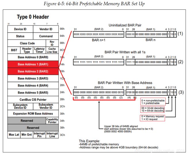
-
In this example, as shown in Figure 4‐5 , BAR1 and BAR2 are being used to request a
64MBblock of prefetchable memory address space. -
Two sequential BARs are being used here because the device supports a 64‐bit address for this request, meaning that software can allocate the requested address space above the 4GB address boundary if it wants to.
-
From the Figure 4‐5, we see the uninitialized state of the BAR pair. The
device designerhas hard‐coded the lower bits of the lower BAR (BAR1 in our example) to indicate the request type and size, while the bits of the upper BAR (BAR2) are all read‐write. -
System software’s first step is to write all 1s to every BAR.
-
System software’s next step is to read the next BAR (BAR1) and evaluate it to see if the device is requesting additional address space. Once BAR1 is read, software realizes that more address space is being requested and this request is for prefetchable memory address space that can be allocated anywhere in the 64‐bit address range. Since it supports a 64‐bit address, the next sequential BAR (BAR2 in this case) is treated as the upper 32 bits of BAR1.
-
System software’s final step is to allocate an address range to the BARs(
2_4000_0000h ‐ 2_43FF_FFFFh) -
总结:系统软件首先往BAR里面写”1“,然后读取BAR,如果BAR中位的没有任何变化,就表明该位是designer硬编码的,就可以推断出映射的空间。本例中BAR写1后,低26位没有任何变化,表明地址空间为2^26 B(64MB).
3.2.2.3 IO Address Space Request

- System software has previously written all 1s to every BAR and has evaluated BAR0, then BAR1 and BAR2.
- Software now reads in BAR3 to evaluate the size and type of the request.
- The final step is to program the BAR with the base address of the IO address range being allocated to this device, specifically this BAR. The device will accept and respond to IO transactions within the range
4000h ‐ 40FFh.
3.2.2.4 All BARs Must Be Evaluated Sequentially
- Most of the time, functions do not need all six BARs.
- Even in the examples we went through, only four of the six available BARs were used. If the function in our example did not need to request any additional address space, the device designer would
hard‐codeall bits of BAR4 and BAR5 to 0s. - So even though software writes those BARs with all 1s, the writes have no affect.
3.2.3 Base and Limit Registers
Each bridge (or switch ports or root complex ports)needs to know what address ranges live beneath it so it can determine which requests should be forwarded from its primary interface (upstream side) to its secondary interface (downstream side).- If the request is targeting an address that is owned by a BAR in a function beneath the bridge, the request should be forwarded to the bridge’s secondary interface.
It is the Base and Limit registers in the Type 1 headersthat are programmed with the range of addresses that live beneath this bridge. - There are the three sets of Base and Limit registers found in each Type 1 header.Three sets of registers are needed because there can be three separate address ranges living below a bridge:
Prefetchable Memory space (P‐MMIO)

- 试想如果我们的
Prefetchable Memory space是0x2_4000_0000h~0x2_43FF_FFFFh,我们应该怎么填写Type1 Header 中Prefetchable Memory Base和Limit相应的位呢? - 填写Prefetchable Memory Base Upper 32 Bits和Prefetchable Memory Base. 首先选取基地址0x2_4000_0000h的
高32位(bit32~bit63)填写到Prefetchable Memory Base Upper 32 Bits中, 然后将基地址低31位中的bit20~bit31位填写到Prefetchable Memory Base中的bit15 ~ bit4位。 - 填写Prefetchable Memory Limit Upper 32 Bits和Prefetchable Memory Limit.首先选取尾地址的0x2_43FF_FFFFh的
高32位(bit32~bit63)填写到Prefetchable Memory Limit Upper 32 Bits中, 然后将基地址低31位中的bit20~bit31位填写到Prefetchable Memory Limit中的bit15 ~ bit4位。
Non‐Prefetchable Memory space(NP‐MMIO)

- 试想如果我们的
Non-Prefetchable Memory space是0xF900_0000h~0xF90F_FFFFh,我们应该怎么填写Type1 Header 中Non-Prefetchable Memory Base和Limit相应的位呢? - 填写Non-Prefetchable Memory Base. 首先选取基地址0xF900_0000h中的
bit20~bit31位填写到Non-Prefetchable Memory Base中的bit15 ~ bit4位。 - 填写Non-Prefetchable Memory Limit .首先选取尾地址的0xF90F_FFFFh中的
bit20~bit31位填写到Non-Prefetchable Memory Limit中的bit15 ~ bit4位。
IO space (IO)
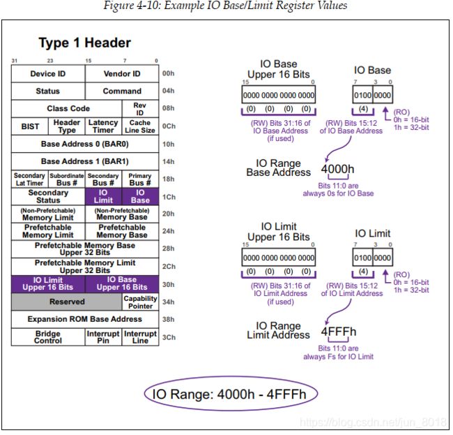
- 试想如果我们的
IO space是0x4000h~0x4FFFh,我们应该怎么填写Type1 Header 中IO Base和Limit相应的位呢? - 填写和
IO Base和IO Base Upper 16Bits. 首先选取基地址0x4000h中的bit16~bit31位填写到IO Base Upper 16Bits中,然后取0x4000的bit15~bit12放到IO Base中bit7-bit4 中。 - 填写和
IO Limit和IO LimitUpper 16Bits. 首先选取基地址0x4FFFh中的bit16~bit31位填写到IO Base Upper 16Bits中,然后取0x4FFF的bit15~bit12放到IO Base中bit7-bit4 中。
3.3 TLP Routing Basics
- PCIe Links are point‐to‐point, more routing will be needed to deliver transactions between devices.
- PCIe topology consists of independent, point‐to‐point links connecting each device with one or more neighbors.
- As traffic arrives at the inbound side of a link interface (called the ingress port), the port checks for errors, then makes one of
three decisions:
- Accept the traffic and use it internally.
- Forward the traffic to the appropriate outbound (egress) port.
- Reject the traffic because it is neither the intended target, nor an interface to it.
- The receiver interface of each device (ingress port) must detect and evaluated the arrival of the three types of link traffic: Ordered Sets, Data Link Layer Packets (DLLPs), and Transaction Layer Packets (TLPs).
Ordered Sets and DLLPsare local to a link and thus are never routed to another link.TLPscan and do move from link to link, based onrouting information contained in the packet headers. - Devices with multiple ports, like
Root Complexes and Switches, can forward TLPs between the ports and are sometimes called Routing Agents or Routing Elements. They accept TLPs that target internal resources and forward TLPs between ingress and egress ports. Endpointshave only one Link and never expect to see ingress traffic other than what is targeting them. They simply accept or reject incoming TLPs.
3.3.1 Three Methods of TLP Routing
- TLPs can be routed following three methods.Table 4‐7 on page 147 summarizes the TLP types and the routing methods used for each.
- based on
address (either memory or IO),- based on
ID (meaning Bus, Device, Function number),routed implicitly.

- Most of the message TLPs defined in the PCI Express spec use implicit routing, however, the vendor‐defined messages could use address routing or ID routing if desired.
3.3.2 Purpose of Implicit Routing and Messages
-
Why Messages? -
Message transactions were introduced with PCIe. The main reason for adding Messages as a packet type was to pursue the PCIe design goal to drastically reduce the number of sideband signals implemented in PCI (e.g. interrupt pins, error pins, power management signals, etc.). Consequently, most of the sideband signals were replaced with in‐band packets in the form of Message TLPs.
-
Implicit routing takes advantage of the fact that Switches and other routing elements understand the concept of upstream and downstream, and that the Root Complex is found at the top of the topology while Endpoints are found at the bottom.
3.3.3 Split Transaction Protocol
- PCI Express uses the split transaction protocol which allows a target device to
receive one or more requests and then respond to each request with a separate completion. This is a significant improvement over the PCI bus protocol that used wait‐states or delayed transactions (retries) to deal with latencies in accessing targets.
3.3.4 Posted versus Non-Posted
non‐postedtransactions require a completion.postedtransactions do not require, and should never receive, a completion.

总结:- 学习PCIe基本概念.
- 学习Configuration Space的种类和访问方式.
- 学习寻址空间的种类和三种传输路由.