PCI Verilog IP 设计
1 PCI IP设计
虽然PCI已经逐渐淘汰,但是还是有不少应用需要这样的接口通讯。
设计目的是为了提供基于源码的PCI IP,这样硬件就不必受限于某一个FPGA型号,也方便ASIC迁移。由于PCI的电气标准都是标准3.3V电平,不像PCIe需要高速收发器、8b/10b编码等技术的支持,因此设计一个基于源码的PCI IP是完全可行的,并且我们设计的IP也确实经过了验证。
1.1 功能需求
l 接收FPGA其它模块的参数设置,由外部参数决定何时启动、停止PCI数据传输
l 兼容PCI 2.2 协议,33Mhz主频,32bit地址/数据
l 工作在Target模式,可接收数据读写、寄存器读写
l 总线状态监测,具备错误汇报能力,并根据错误类型决定后续动作,比如重试、停止当前传输
1.2 IP特性
l 标准32位33Mhz PCI Target接口;
l Wishbone master接口,支持block/burst读写;
l 数据均使用小端模式,可以方便在windows上进行存储,符合常用习惯;
l 具备标准PCI配置寄存器空间,参数支持修改;
l BAR0 register, 在PCI memory map空间占据32Mbytes;
l 需要支持的PCI指令如下:
0110 Memory Read
0111 Memory Write
1010 Configuration Read
1011 Configuration Write
1100 Memory Read Multiple
1110 Memory Read Line
1111 Memory Write and Invalidate
l 支持对PCI读写进行重试,用户可通过wishbone master接口发起;
1.3 接口定义/引脚描述
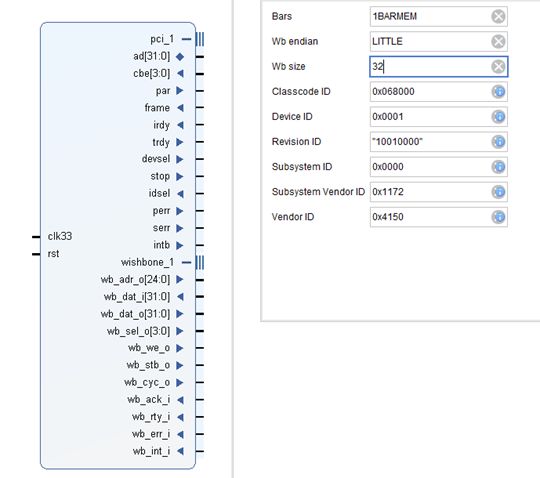
图 5‑1 PCI Core接口与参数列表(在VIVADO中的形式)
接口主要分成2个部分:
l PCI target接口;
l Wishbone master接口;
参数说明:
l Bars “1BARMEM"/"1BARIO",支持memory 模式和IO模式,推荐使用默认memory模式;
l Wb endian: wishbone总线使用大端还是小端模式,推荐使用默认小端模式;
l Wb size: wishbone bus size,推荐使用默认32 ;
l Class code ID: PCI class code id;
l Device ID: PCI device id,可以自由指定,当前设备的ID;
l Revision ID: PCI Revision ID,可以自由指定,当前固件的版本;
l Subsystem ID: 子系统ID,一般和Device ID相同,也可以不同;
l Subsystem Vendor ID: 子系统厂商ID,由用户指定,一般会和Vendor ID相同;
l Vendor ID: PCI提供商ID,表面设备生产厂商,正式的Vendor ID需要向PCI SIG申请,但是在特定系统使用时,可以由用户自己指定,只要不和现有设备冲突即可;
因为CPU依靠Vendor ID和Device ID来区分不同类型的设备。
接口类型声明
引脚输入输出方向:
In standard input only
out standard output only
t/s Tri-State is a bi-directional, tri-state input/output pin
s/t/s 在时序上要对这类信号多加注意,避免时序出错。Sustained Tri-State is an active low tri-state signal owned and driven by one and only one agent at a time. The agent that drives an s/t/s pin low must drive it high for at least one clock before letting it float. A
new agent cannot start driving a s/t/s signal any sooner than one clock
after the previous owner tri-states it. A pullup is required to sustain
the inactive state until another agent drives it and must be provided by
the central resource.
o/d Open Drain allows multiple devices to share as a wire-OR. A pull-up is required to sustain the inactive state until another agent drives it and must be provided by the central resource.
1.3.1 内部用户接口
内部接口即用户接口,是wishbone master接口,本小节介绍接口定义与关键时序。
| 名称 |
方向 |
分组 |
定义 |
| wb_adr_o |
out |
Internal pins |
Whisbone address |
| wb_dat_i |
in |
Internal pins |
Whisbone data in |
| wb_dat_o |
out |
Internal pins |
Whisbone data out |
| wb_sel_o |
out |
Internal pins |
Whisbone data byte selection . The select output array [SEL_O()] indicates where valid data is expected on the [DAT_I()] signal array during READ cycles, and where it is placed on the [DAT_O()] signal array during WRITE cycles. 表征当前bit对应的byte数据有效,数据周期一般是0xf,表示32bit数据全部有效 |
| wb_we_o |
out |
Internal pins |
Whisbone write enable. The write enable output [WE_O] indicates whether the current local bus cycle is a READ or WRITE cycle. The signal is negated during READ cycles, and is asserted during WRITE cycles. 表征当前操作是读还是写 |
| wb_stb_o |
out |
Internal pins |
Whisbone data strobe. The strobe output [STB_O] indicates a valid data transfer cycle. It is used to qualify various other signals on the interface such as [SEL_O()]. The SLAVE asserts either the [ACK_I], [ERR_I] or [RTY_I] signals in response to every assertion of the [STB_O] signal 数据有效标志 |
| wb_cyc_o |
out |
Internal pins |
Whisbone cycle. The cycle output [CYC_O], when asserted, indicates that a valid bus cycle is in progress. The signal is asserted for the duration of all bus cycles. For example, during a BLOCK transfer cycle there can be multiple data transfers. The [CYC_O] signal is asserted during the first data transfer, and remains asserted until the last data transfer. 会在整个数据传输周期保持有效 |
| wb_ack_i |
in |
Internal pins |
Whisbone acknowledge. The acknowledge input [ACK_I], when asserted, indicates the normal termination of a bus cycle.如果是block传输,则可能一直有效 |
| wb_rty_i |
in |
Internal pins |
Whisbone retry. The retry input [RTY_I] indicates that the interface is not ready to accept or send data, and that the cycle should be retried. Slave要求master重试 |
| wb_err_i |
in |
Internal pins |
Whisbone error. The error input [ERR_I] indicates an abnormal cycle termination. |
| wb_int_i |
in |
Internal pins |
Whisbone interrupt. 中断引脚,实际并不使用 |
1.3.2 Wish bone读写时序
图 5‑2 PCI通过wishbone接口进行单次读取,这里可以用做读写用户寄存器,wb_stb_o&wb_cyc_o==1时,当前读请求有效,slave在下一个时钟周期进行回应,同时返回指定地址的数据
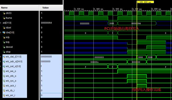
图 5‑3 PCI通过wishbone接口进行单次写入,这里可以用做用户寄存器写入,wb_stb_o&wb_cyc_o==1时,当前读请求有效,slave在下一个时钟周期进行回应,表面请求写入的动作已经完成。
图 5‑4 PCI block read方式读,可以用做DMA数据读取,PCI的读操作转换成wishbone的读操作,wb_stb_o&wb_cyc_o==1时,当前读请求有效,在下一个时钟周期返回有效数据,最后一个周期的读请求无需响应。
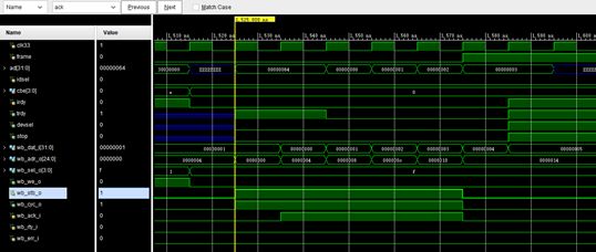
图 5‑5 PCI block write方式写入,可以用做DMA数据写入,PCI的读操作转换成wishbone的写操作,wb_stb_o&wb_cyc_o==1时,当前写请求有效,在下一个时钟周期返回写完成相应,最后一个周期的写请求无需响应。
1.3.3 PCI物理接口
参考来自PCI SPEC V2.2
表 5‑3 PCI接口
| 名称 |
方向 |
分组 |
定义 |
| clk33 |
in |
System pins |
Clock provides timing for all transactions on PCI and is an input to every PCI device. All other PCI signals, except RST#, INTA#, INTB#, INTC#, and INTD#, are sampled on the rising edge of CLK and all other timing parameters are defined with respect to this edge 该信号应来自板载晶振 |
| rst |
in |
System pins |
Reset is used to bring PCI-specific registers, sequencers, and signals to a consistent state. Anytime RST# is asserted, all PCI output signals must be driven to their benign state. In general, this means they must be asynchronously tri-stated. REQ# and GNT# must both be tristated (they cannot be driven low or high during reset). To prevent AD, C/BE#, and PAR signals from floating during reset, the central resource may drive these lines during reset (bus parking) but only to a logic low level; they may not be driven high. 该信号来自板载复位 |
| ad [31:0] |
t/s |
Address and Data Pins |
Address and Data are multiplexed on the same PCI pins. A bus transaction consists of an address2 phase followed by one or more data phases. PCI supports both read and write bursts. |
| cbe [3:0]# |
t/s |
Address and Data Pins |
Bus Command and Byte Enables are multiplexed on the same PCI pins. During the address phase of a transaction, C/BE[3::0]# define the bus command (refer to Section 3.1. for bus command definitions). During the data phase, C/BE[3::0]# are used as Byte Enables |
| par |
t/s |
Address and Data Pins |
Parity is even parity across AD[31::00] and C/BE[3::0]#. Parity generation is required by all PCI agents. Parity generation is not optional, it must be done by all PCI-compliant devices 偶检验是必须实现的功能 |
| frame# |
s/t/s |
Interface Control Pins |
Cycle Frame is driven by the current master to indicate the beginning and duration of an access. FRAME# is asserted to indicate a bus transaction is beginning. While FRAME# is asserted, data transfers continue. When FRAME# is deasserted, the transaction is in the final data phase or has completed. 读写时序图上可以看到传输是如何结束的 |
| irdy# |
s/t/s |
Interface Control Pins |
Initiator Ready indicates the initiating agent’s (bus master’s) ability to complete the current data phase of the transaction. IRDY# is used in conjunction with TRDY#. A data phase is completed on any clock both IRDY# and TRDY# are asserted. During a write, IRDY# indicates that valid data is present on AD[31::00]. During a read, it indicates the master is prepared to accept data. Wait cycles are inserted until both IRDY# and TRDY# are asserted together. |
| trdy# |
s/t/s |
Interface Control Pins |
Target Ready indicates the target agent’s (selected device’s) ability to complete the current data phase of the transaction. TRDY# is used in conjunction with IRDY#. A data phase is completed on any clock both TRDY# and IRDY# are asserted. During a read, TRDY# indicates that valid data is present on AD[31::00]. During a write, it indicates the target is prepared to accept data. Wait cycles are inserted until both IRDY# and TRDY# are asserted together. |
| stop |
s/t/s |
Interface Control Pins |
Stop indicates the current target is requesting the master to stop the current transaction. |
| devsel |
s/t/s |
Interface Control Pins |
Device Select, when actively driven, indicates the driving device has decoded its address as the target of the current access. As an input, DEVSEL# indicates whether any device on the bus has been selected. |
| idsel |
in |
Interface Control Pins |
Initialization Device Select is used as a chip select during configuration read and write transactions. |
| perr# |
s/t/s |
Error Reporting Pins |
Parity Error is only for the reporting of data parity errors during all PCI transactions except a Special Cycle. The PERR# pin is sustained tri-state and must be driven active by the agent receiving data (when enabled) two clocks following the data when a data parity error is detected. The minimum duration of PERR# is one clock for each data phase that a data parity error is detected. |
| serr# |
o/d |
Error Reporting Pins |
System Error is for reporting address parity errors, data parity errors on the Special Cycle command, or any other system error where the result will be catastrophic. |
| intb# |
o/d |
Interrupt Pins |
Interrupt C is used to request an interrupt and only has meaning on a multi-function device 本项目不会使用该引脚 |
下面是客户提供的名称,其中REQ和GNT是Master专用,本设计实际并不需要
- STOP
- SERR
- PERR
- RST
- FRAME
- TRDY
- DEVSEL
- PAR
- CLK
- INTC
- REQ[3:0] Bus Masters Only,因此不需要
- GNT[3:0] Bus Masters Only,因此不需要
- CBE[3:0]
- AD[31:0]
1.4 状态机
本部分参考PCI SPEC V2.2中参考状态机进行修改设计。
以下是spec对状态机的描述
“Caution needs to be taken when an agent is both a master and a target. Each must have its own state machine that can operate independently of the other to avoid deadlocks. This means that the target state machine cannot be affected by the master state machine. Although they have similar states, they cannot be built into a single machine.”
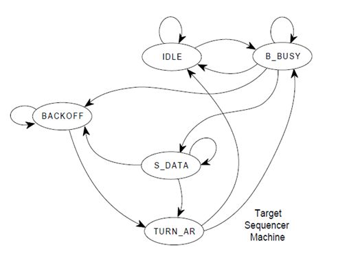
图 5‑6 PCI Core状态机示意图,实际会多出2个状态
实际为了将PCI操作转化为Wishbone读写,状态S_DATA2和TURN_ARE状态,这两个状态主要目的是满足信号时序逻辑。
状态机状态:PCIIDLE, B_BUSY, S_DATA1, S_DATA2, BACKOFF, TURN_ARL, TURN_ARE。详细跳转过程可以参照代码进行理解,文档对该部分暂时不做详细说明。
1.5 PCI关键时序
该部分将用时序图的方式,分别对PCI的各种操作给出PCI Spec要求的时序、以及本项目提供的PCI Core实际仿真时序。其中仿真时序中IRDY信号并未严格满足要求(该信号来源于PCI master,本文档不需要提供PCI master,只是提供仿真模型),但是并不影响实际结果。
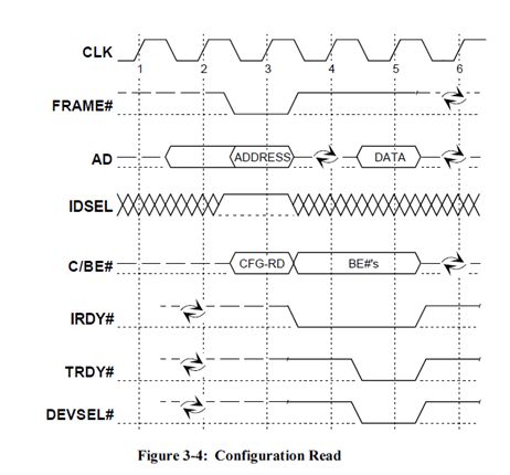
图 5‑7 读配置寄存器
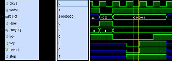
图 5‑8 读取device id 0x0001,vendor id 0x4150,各占用16bit,其中vendor id占用低16bit,当前图示时序的irdy比理论多出一个有效的时钟周期,这只是仿真逻辑pci master的问题,且并不影响数据传输的正确性,因此可以忽略
图 5‑9 写入PCI配置寄存器,base address registers, 地址0x10,写入数据0x3000_0000
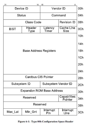
图 5‑10 PCI 配置寄存器列表
图 5‑11 从用户地址空间读取用户寄存器
图 5‑12 向用户地址空间写入寄存器
图 5‑13 从用户地址空间以block的方式读出数据
图 5‑14 向用户地址空间以block的方式写入数据
在仿真代码中,加入对寄存器读写的测试。
start_read =0;
addr =0;
length=1;
rst=1;
#200;
rst=0;
//vendor id device id
pci_configuration_read(0,data_value);
assert(data_value=='h14150);
//cmd status
pci_configuration_read(4,data_value);
assert(data_value=='h02000002);
pci_configuration_write('h10,'h3000_0000);
pci_configuration_read(0,data_value);
assert(data_value=='h14150);
pci_configuration_read('h10,data_value);
assert(data_value=='h3000_0000);
pci_memory_read('h3000_0000,data_value);
assert(data_value==0);
pci_memory_read('h3000_0004,data_value);// address add 4 every time, must increment WBSIZE/8
assert(data_value==1);
pci_memory_read('h3000_0008,data_value);// address add 4 every time
assert(data_value==2);
pci_memory_write('h3000_0000,100);
pci_memory_read('h3000_0000,data_value);
assert(data_value==100);
pci_memory_write('h3000_0000,0);//重新写0
pci_memory_read_line('h3000_0000,4,data_value);//read line
pci_memory_write_line('h3000_0000,4,111);//write line
pci_memory_read_line('h3000_0000,4, data_value);//read line
pci_memory_read_line('h3000_0000,5, data_value);//read line
pci_memory_read_line('h3000_0000,6, data_value);//read line
pci_memory_read_line('h3000_0010,10, data_value);//read line
1.6 支持的PCI指令
l 支持的PCI指令
0110 Memory Read
0111 Memory Write
1010 Configuration Read
1011 Configuration Write
1100 Memory Read Multiple
1110 Memory Read Line
1111 Memory Write and Invalidate
下面是一些spec对相关指令的描述,用户并不需要特别关注下面的内容,这只是开发人员的记录。
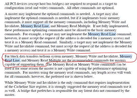
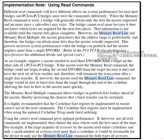
从上面这段话可以看出,单纯的memory read 是一次只能读取4个字节,效率很低。
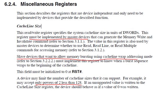
而memory read line/ memory read multiple自治领推荐实现cache line size 寄存器。下面这段话可以看出cache line size 寄存器所起的作用和约束。
It is highly recommended that the Cacheline Size register be implemented to ensure
correct use of the read commands. 这个只是针对master设备而言,target设备只负责接收请求。
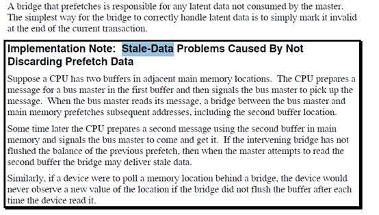
Bridge会读取比master更多的数据来实现高性能数据传输。
那么bridge是有责任负责存储预取的隐藏数据责任,最简单的方式是认为该部分数据无效并抛弃,需要注意,这样的方式不进行小心的处理可能导致数据的丢失。
从6章节关于cache line size寄存器的描述可以看出,对于target类型的slave设备,除非需要支持cacheline wra addressing模式,否则是可以不实现cache line size的,数据的传输大小由master设备决定。
图 5‑15 block read
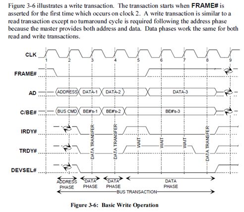
数据传输的终止,取决于master的frame信号,frame信号为高表示要终止传输,下一个数据即最后一个数据。
