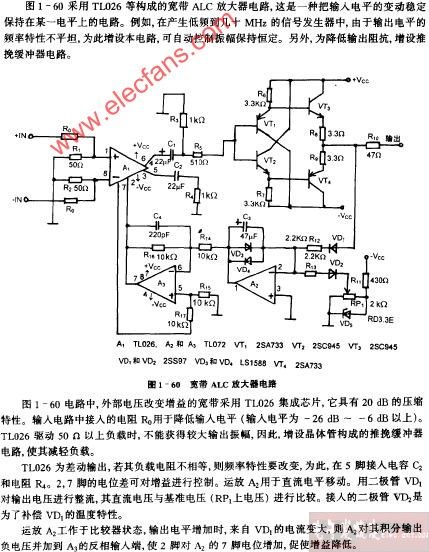
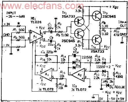
采用TL026等构成的宽带ALC放大器电路图
Building a Differential Amplifier
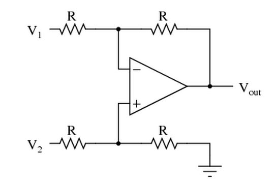
An op-amp with no feedback is already a differential amplifier, amplifying the voltage difference between the two inputs. However, its gain cannot be controlled, and it is generally too high to be of any practical use. So far, our application of negative feedback to op-amps has resulting in the practical loss of one of the inputs, the resulting amplifier only good for amplifying a single voltage signal input. With a little ingenuity, however, we can construct an op-amp circuit maintaining both voltage inputs, yet with a controlled gain set by external resistors.
If all the resistor values are equal, this amplifier will have a differential voltage gain of 1. The analysis of this circuit is essentially the same as that of an inverting amplifier, except that the noninverting input (+) of the op-amp is at a voltage equal to a fraction of V2, rather than being connected directly to ground. As would stand to reason, V2 functions as the noninverting input and V1 functions as the inverting input of the final amplifier circuit. Therefore:
If we wanted to provide a differential gain of anything other than 1, we would have to adjust the resistances in both upper and lower voltage dividers, necessitating multiple resistor changes and balancing between the two dividers for symmetrical operation. This is not always practical, for obvious reasons.
Another limitation of this amplifier design is the fact that its input impedances are rather low compared to that of some other op-amp configurations, most notably the noninverting (single-ended input) amplifier. Each input voltage source has to drive current through a resistance, which constitutes far less impedance than the bare input of an op-amp alone. The solution to this problem, fortunately, is quite simple. All we need to do is “buffer” each input voltage signal through a voltage follower like this:
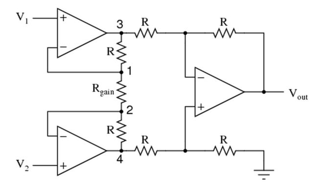
Now the V1 and V2 input lines are connected straight to the inputs of two voltage-follower op-amps, giving very high impedance.
The two op-amps on the left now handle the driving of current through the resistors instead of letting the input voltage sources
(whatever they may be) do it. The increased complexity to our circuit is minimal for a substantial benefit.
The Instrumentation Amplifier
As suggested before, it is beneficial to be able to adjust the gain of the amplifier circuit without having to change more than one resistor value, as is necessary with the previous design of differential amplifier. The so-called instrumentationbuilds on the last version of differential amplifier to give us that capability:
This intimidating circuit is constructed from a buffered differential amplifier stage with three new resistors linking the two buffer circuits together.
Consider all resistors to be of equal value except for Rgain.
The negative feedback of the upper-left op-amp causes the voltage at point 1 (top of Rgain) to be equal to V1.
Likewise, the voltage at point 2 (bottom of Rgain) is held to a value equal to V2.
This establishes a voltage drop across Rgain equal to the voltage difference between V1 and V2.
That voltage drop causes a current through Rgain, and since the feedback loops of the two input op-amps draw no current,
that same amount of current through Rgain must be going through the two “R” resistors above and below it.
This produces a voltage drop between points 3 and 4 equal to:
The regular differential amplifier on the right-hand side of the circuit then takes this voltage drop between points 3 and 4, and amplifies it by a gain of 1 (assuming again that all “R” resistors are of equal value). Though this looks like a cumbersome way to build a differential amplifier, it has the distinct advantages of possessing extremely high input impedances on the V1 and V2 inputs (because they connect straight into the noninverting inputs of their respective op-amps), and adjustable gain that can be set by a single resistor. Manipulating the above formula a bit, we have a general expression for overall voltage gain in the instrumentation amplifier:
hough it may not be obvious by looking at the schematic, we can change the differential gain of the instrumentation amplifier simply by changing the value of one resistor: Rgain. Yes, we could still change the overall gain by changing the values of some of the other resistors, but this would necessitate balanced resistor value changes for the circuit to remain symmetrical. Please note that the lowest gain possible with the above circuit is obtained with Rgain completely open (infinite resistance), and that gain value is 1.
An instrumentation amplifier is a differential op-amp circuit providing high input impedances
with ease of gain adjustment through the variation of a single resistor.
Voltage Definitions
To understand the behavior of a fully-differential amplifier, it is important to understand the voltage definitions used to describe the amplifier.
Figure 3 shows a block diagram used to represent a fully-differential amplifier and its input and output voltage definitions.
The voltage difference between the plus and minus inputs is the input differential voltage, Vid.
The average of the two input voltages is the input common-mode voltage, Vic.
The difference between the voltages at the plus and minus outputs is the output differential voltage, Vod.
The output common-mode voltage, Voc, is the average of the two output voltages, and is controlled by the voltage at Vocm.
With a(f) as the frequency-dependant differential gain of the amplifier, then Vod = Vid × a(f).
Basic Circuits
In a fully-differential amplifier, there are two possible feedback paths in the main differential amplifier, one for each side.
This naturally forms two inverting amplifiers, and inverting topologies are easily adapted to fully-differential amplifiers.
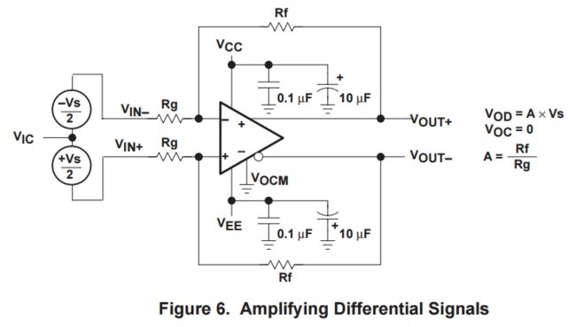
Figure 6 shows how to configure a fully-differential amplifier with negative feedback to control the gain and maintain a balanced amplifier.
Symmetry in the two feedback paths is important to have good CMRR performance.
CMRR is directly proportional to the resistor matching error—a 0.1% error results in 60 dB of CMRR.
The Vocm error amplifier is independent of the main differential amplifier.
The action of the Vocm error amplifier is to maintain the output common-mode voltage at the same level as the voltage input to the Vocm pin.
With symmetrical feedback, output balance is maintained, and Vout+ and Vout– swing symmetrically around the voltage at the Vocm input.
Generation of differential signals has been cumbersome in the past.
Different means have been used, requiring multiple amplifiers.
The integrated fully-differential amplifier provides a more elegant solution.
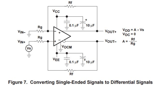
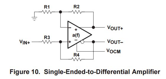
Figure 7 shows an example of converting single-ended signals to differential signals.
A simple IF AGC circuit that features wide dynamic range and excellent linearity can be achieved with two chips:
Tl's TL026C voltage-controlled amplifier IC and Linear Technology's LT1014 (or any other similar basic quad op amp).
具有50MHZ/-3DB带宽、20DB压缩特性的宽带ALC放大器电路的功能
这是一种将输入电平不稳定的信号稳定在一定电平上的电路,用于性能要求高的电路中,在这些信号发生器中,由于频率特性不平坦,输出电平会有波动,
如果加入本电路,则能进行自动控制,使信号保持一定的振幅。此外,为了降低输出阻抗,电路加了推挽冲级。
电路工作原理
本电路采用了可由外部电压控制放大倍数的宽带放大器IC,从而具有20DB的压缩特性。输入电路中,带有★标记的电阻是为降低输入电平而加的,
驱动50欧负载时,因为TL026难以获得较大的输出振幅,所以在电路中增加了由晶体管组成的推挽缓冲放大器,以减轻TL026的负担。
TL026的输出为差动式,如果负载电阻不相等,频率特性就会发生变化,所以在引线上接了C2和R4。
引线2.7之间的电位差可对放大倍数进行控制,因为直流漂移,所以用了OP放大器。
二极管D1对输出进行整流,并与基准电压进行比较。二极管D2是为了补偿D1的温度特性而加的。
OP放大器A2起到比较电路的作用,当输出电平升高时,流过D1的电流就会加大,A2将其积分后输出负电压,
并加在A3的反相输入端,使A2的引线2相对于A1的引线7的电位有增加,从而使A1的放大倍数下降。
元件的选择
因为整个电路形成ALC环路,所以元件的选用比较容易,但是产生基准电压的二极管D5、可变电阻VR1、电阻R12、R13的稳定性则是选用元件时应重点考虑的问题。
为了使二极管D1和D2的正向电压相等,应采用热耦合。普通小信号开关二极管,50MHZ时其整流特性会有所下降,所以,应选用肖特基二极管。
调整和电气特性
不加带★标记的电阻,输入-20DBM,F=1MHZ左右的信号,调整VR1,输出端获得1VP-P的电压。
再将输入电压放大10DB,验证输出有无变化。
Can I use TL026 as an input amplification stage for a 10-bit ADC and use PWM with RC filter to generate the gain control signal? Thanks.
The PWM is generated based on ADC output.
Hello Frank,
The AGC can be run from the filtered PWM signal. Keep in mind the limited AGC range, Vref-180mV < Vagc < Vref+180mV.
This is shown in both figure 5 on page 4 and the 'Gain Characteristics' on page 5.
Regards, Ron Michallick
Gain characteristics
Figure 5 shows the differential voltage amplification versus the differential gain-control voltage (VAGC – Vref).
VAGC is the absolute voltage applied to the AGC input and Vref is the dc voltage at the REF OUT output.
As VAGC increases with respect to Vref, the TL026C gain changes from maximum to minimum.
As shown in Figure 5 for example, VAGC would have to vary
from approximately 180 mV less than Vref to approximately 180 mV greater than Vref to change the gain from maximum to minimum.
The total signal change in VAGC is defined by the following equation.
∆VAGC = (Vref + 180 mV) – (Vref – 180 mV)
∆VAGC = 360 mV (1)
However, because VAGC varies as the ac AGC signal varies and also differentially around Vref,
then VAGC should have an ac signal component and a dc component.
To preserve the dc and thermal tracking of the device, this dc voltage must be generated from Vref.
To apply proper bias to the AGC input, the external circuit used to generate VAGC must combine these two voltages.
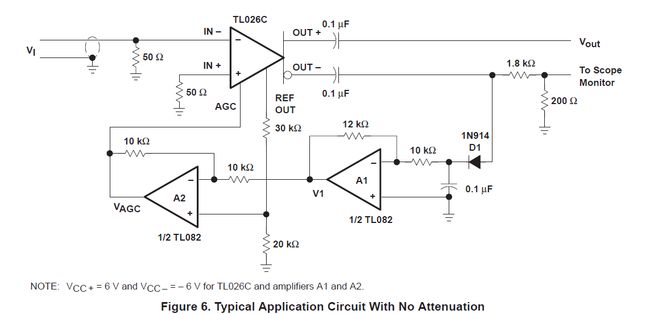
Figures 6 and 7 show two circuits that will perform this operation and are easy to implement.
The circuits use a standard dual operational amplifier for AGC feedback.
By providing rectification and the required feedback gain, these circuits are also complete AGC systems.
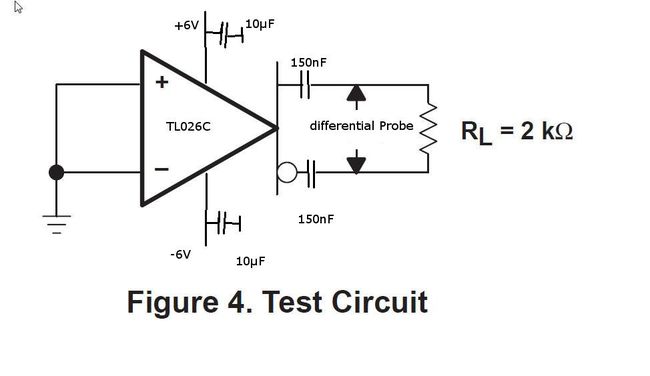
tl026 noise when input aty GND
my customer uses the TL026C with differencial output and input to GND with +/-6V.
the output is connected to two serial cap of 150nF and with 2 K load.
the output is pretty noisy, could you explainit?
i have the sch and plots.
Kamal,
The output is floating.
Try replacing the 2k resistor with two 1k resistors in series then ground the node between the resistors.
Measure noise. Then turn power to TL026 off and measure noise again (power off noise, not caused by TL026).
Ronald Michallick
Linear Applications
采 用 TL026C 的视 频 光 接 收 机 中 AGC放大 电路设计
TL026C是美 国 TI公 司生产 的一 种具有 自动增 益 控 制 (AutomaticGainControl,AGC)功 能 的差 分 高 频 放大器。
其增益的改变由AGC管脚电压控制,相对于 基准 电 压(REFOUT)对 AGC端输 入+200mv电压 ,可 得到 50dB范 围的可变增 益 。
TLD26C广泛应用在要 求 宽频带 、低 相位偏 差及优 良增益稳 定性 的视 频和脉 冲 放大 电路 。
TL026C 的 AGC 实现 原 理 TL026C内部 AGC反馈电路使输出信号具有宽频带 、低相位偏 差及优 良的增益 稳定性 。
芯 片增益 的改 变随 AGC管脚 的控制 电压 而改变 ,相对 于基准 电压有 50dB范 围的可变增益 。
其增益与差分控 制电压(V — V )的关系如 图 1所示 。其 中 Vagc是 TL026C的 AGC 管脚 电压 ,
Vref 是 REFOUT管脚 输 出 的直 流 电压 ,是 一 个参 考 电压 ,其 电压值 恒 定 ,不 随芯片 的输 出电压 大小改变 。
当 相对 于 Vagc 改变时 ,TL026C芯 片增 益改变 。 由图 2可看 到 , Vagc 的值从 一180mv左右 to +180mv左 右时 ,芯片增益 由最大变 到最小 。
即Vagc 当 相对 与基 准 电压 Vref 增 大时 ,芯 片增 益 减小 ;反 之 ,芯片增益增 大 。
以此 种方法来 实现对输 出信号增 益 的 自动控 制 , 进 而使 其输 出信号保持在一个恒 定的范围 内。
AGC电路 注意事项
检波二极 管的导通 电压决定 AGC电路 的 门限 检波 电压 。
硅 管的导通 电压大约是 0.7V。因此 ,根据输 出 ,所选二 极管必须使输 出信号有 足够的幅度通过 。
由于 TL026C芯 片 内部 电路 的限 制 ,其最大 信 号输 出峰一峰值不超过 3V。
