iMX6平台MAX9288调试
因为有之前Ti ds90ub864的调试经验,这次调9288只是当做一个常规的驱动调试,坑大也得到了宝贵的经验
9288(GMSL--->MIPI CSI2)解码器解码9291和9277编码器过来的gmsl信号
iMX6DQ的mipi csi接口寄存器控制的特性:
IPU0-CSI0: can be connected to parallel interface(GPR1 bit19 is 1) or to mipi-csi2 virtual channel0(GPR1 bit19 is 0).
IPU0-CSI1: can only be connected to mipi-csi2 virtual channel1.
IPU1-CSI0: can only be connected to mipi-csi2 virtual channel2.
IPU1-CSI1: can be connected to parallel interface(GPR1 bit20 is 1) or to mipi-csi2 virtual channel3(GPR1 bit 20 is 0).
基于官方评估板和原始官方代码,选择串行还是并行的控制寄存器GPR1非常重要,控制这两个并口和一个串行接口的选择;还有由于写代码人的随意,官方ov5640_mipi中virtual channel的选择的是根据dts里的csi_id来判断的
由于ov5640的芯片同时有两种接口parallel interface和mipi-csi2,官方代码里有两个方法从默认的parallel interface改为mipi-csi2
1. 使用mipi-csi2接口的vc1通道,只需删除如下dts即可
v4l2_cap_0 {
	compatible = "fsl,imx6q-v4l2-capture";
	ipu_id = <0>;
	csi_id = <0>;
	mclk_source = <0>;
	status = "okay";
};
2. 使用mipi-csi2接口的vc0通道,需要更改dts和将GPR1将IPU0-CSI0连接到mipi-csi2 virtual channel0(GPR1 bit19 is 0)
将dts中的相应的csi_id = <1>改为csi_id = <0>
更改GPR1寄存器,位于arch/arm/mach-imx/mach-imx6q.c文件,将bit19置为0
如需要使用vc3则把bit20也置0,在这里第三个参数为mask已经将19,20位置0了
if (of_machine_is_compatible("fsl,imx6q-sabresd")) {
 			regmap_update_bits(gpr, IOMUXC_GPR1, 3 << 19, 0 << 19);
这两种方法都是打开video0节点,方法1.中该节点是vc1通道,方法2.中该节点是vc0通道,如果更改mxc_v4l2_tvin的应用程序,方法2.的video1节点可以通过打开vc1来与vitrual channel可选的ov5640进行通信
iMX6的mipi csi2初始化也有严格的规范,官方手册IMX6DQRM中40.3.1要求的规范如下
1. Deassert CSI2 presetn signal (global reset);
2. Configure MIPI Camera Sensor to have all Tx lanes in PL-11 state
(STOPSTATE) if required - According to D-PHY Specification the D-PHY master
should be initialized at LP-11 state (STOPSTATE), nevertheless a CCI command
may be required to switch-on the MIPI interface;
3. D-PHY initialization - Access the D-PHY programming interface to initialize and
program the D-PHY according to the selected operating mode of the D-PHY. This is
D-PHY dependent, and this programming should be carried out according to the D-
PHY databook;
4. CSI2 Controller programming - Program the CSI2 Host Controller registers
according to the operating mode required:
• Number of Lanes (register N_LANES);
• Deassert PHY shutdown (register PHY_SHUTDOWNZ);
• Deassert PHY reset (register PHY_RSTZ);
• Deassert CSI reset (register CSI2_RESETN);
i.MX 6Dual/6Quad Applications Processor Reference Manual, Rev. 5, 06/2018
3528
NXP SemiconductorsChapter 40 MIPI - Camera Serial Interface Host Controller (MIPI_CSI)
• (Optional) Program Data IDs for matching error reporting (registers
DATA_IDS_1 and DATA_IDS_2);
• (Optional) Program the interrupt masks (registers MASK1 and MASK2);
5. CSI2 Controller programming - Read the PHY status register (PHY_STATE) to
confirm that all data and clock lanes of the D-PHY are in Stop State (i.e. ready to
receive data);
6. Configure the MIPI Camera Sensor - Access Camera Sensor using CCI interface
to initialize and configure the Camera Sensor to start transmitting a clock on the D-
PHY clock lane;
7. CSI2 Controller programming - Read the PHY status register (PHY_STATE) to
confirm that the D-PHY is receiving a clock on the D-PHY clock lane;
流程图表达式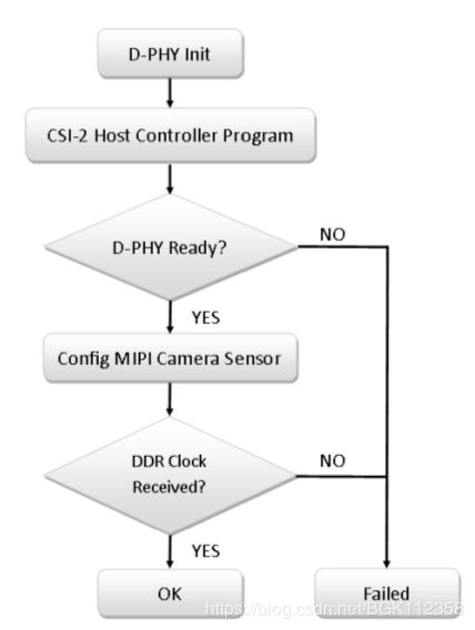
在代码中体现为
mipi_csi2_info = mipi_csi2_get_info();

/* initial mipi dphy */
if (!mipi_csi2_info) {
	printk(KERN_ERR "%s() in %s: Fail to get mipi_csi2_info!\n",
		__func__, __FILE__);
	return -1;
}

if (!mipi_csi2_get_status(mipi_csi2_info))
	mipi_csi2_enable(mipi_csi2_info);

if (!mipi_csi2_get_status(mipi_csi2_info)) {
	pr_err("Can not enable mipi csi2 driver!\n");
	return -1;
}

mipi_csi2_set_lanes(mipi_csi2_info);
mipi_csi2_reset(mipi_csi2_info);
mipi_csi2_set_datatype(mipi_csi2_info, MIPI_DT_RGB888);

/* 启动解码芯片的位置要在这个地方才符合MIPI的初始化规范,否则存在PHY_STATUS异常等问题 */
max9288_registers_init();
max9288_dump_reg();

if (mipi_csi2_info) {
	unsigned int i;
	i = 0;

	/* wait for mipi sensor ready */
	mipi_reg = mipi_csi2_dphy_status(mipi_csi2_info);
	while (((mipi_reg & 0x700) != 0x300) && (i < 10)) {
		mipi_reg = mipi_csi2_dphy_status(mipi_csi2_info);
		i++;
		msleep(10);
	}

	if (i >= 10) {
		pr_err("mipi csi2 can not receive sensor clk! MIPI_CSI_PHY_STATE = 0x%x.\n", mipi_reg);
		return -1;
	}

	i = 0;

	/* wait for mipi stable */
	mipi_reg = mipi_csi2_get_error1(mipi_csi2_info);
	while ((mipi_reg != 0x0) && (i < 10)) {
		mipi_reg = mipi_csi2_get_error1(mipi_csi2_info);
		i++;
		msleep(10);
	}

	if (i >= 10) {
		pr_err("mipi csi2 can not reveive data correctly! MIPI_CSI_ERR1 = 0x%x.\n", mipi_reg);
		return -1;
	}
}
按照这个规范初始化mipi后在关注代码中几个状体寄存器的值,参考论坛的Debug steps for customer MIPI sensor文档
主要关注MIPI_CSI_PHY_STATE和MIPI_CSI_ERR1/2,通常MIPI_CSI_PHY_STATE=0x300,MIPI_CSI_ERR1/2=0x0,这两个寄存器对了基本不会有问题了,在分辨率和时钟等再做细微调整
9288就调试完了,过程是相对简单的,之前因为显示驱动问题一直查capture,做了好些时钟和分辨率的计算,如下做个笔记
MIPI 性能
带宽部分
The maximum MIPI-CSI2 frequency is 200 MHz
Each lane can transfer up to 1000 Mb/s or up to 800 Mb/s when all four lanes are used
The required minimum operating frequency of the interface is calculated as:
F = FH * FW * FPS * BI * DF
Where:
• FH—frame height (in pixels)
• FW—frame width (in pixels)
• FPS—frame rate (frames per second)
• DF—data format; defines the number of cycles needed to send a single pixel
• BI—blank interval; a 35 % (1.35) overhead provides a safe estimate for the minimum frequency
Or as:
the minimum operating frequency can be also calculated as:
F = TFH * TFW * FPS * DF
where:
• TFH—total frame height = front porch + vsync + back porch
• TFW—total frame width = front porch + hsync + back porch
• FPS—frame rate (frames per second)
• DF—data format; defines the number of cycles needed to send a single pixel
• Camera 1—virtual channel 0: 1024x768, 4-lane configuration, 30 fps, YUV422 format:
1024 * 768 * 30 fps * 1 cycle/pixel * 1.35 blank interval = 31.85 MHz
• Camera 2—virtual channel 1: 1920x1080, 4-lane configuration, 30 fps, YUV422 format:
1920 * 1080 * 30 fps * 1 cycle/pixel * 1.35 blank interval = 83.98 MHz
Total bandwidth = 31.85 MHz + 83.98 MHz = 115.83 MHz
更多例子请查看手册MIPI–CSI2 Peripheral on i.MX6 MPUs(AN5305)
MIPI物理层时钟
To calculate the MIPI data rate, use these equations:
MIPI data rate = (MIPI clock * 2) * Number of lanes >= Pixel clock * Bits-per-pixel
MIPI clock = (Pixel clock * Bits-per-pixel) / (Number of lanes) / 2
For example, a video input of 720p, 59.94 fps, and YUV422 is calculated as follows:
Pixel clock = 1280 * 720 * 59.94 fps * 1 cycle/pixel * 1.35 blank interval = 74.57 MHz
Total MIPI data rate is 74.25 M * 16 bits = 1193 Mb/s.
The frame blank intervals and the interface packaging overhead were added as the 1.35 factor in the
pixel clock equation above.
For a 2-lane interface:
MIPI clock = 1193 / 2 / 2 = 298.25 MHz
MIPI_CSI2_PHY_TST_CTRL1 setting = 298.25 MHz * 2 (DDR mode) = 596.5 MHz
According to Table 2, MIPI_CSI2_PHY_TST_CTRL1 = 0x2E.
For a 4-lane interface:
MIPI clock = 1193 / 4 / 2 = 149.12 MHz
MIPI_CSI2_PHY_TST_CTRL1 setting = 149.12 MHz * 2 (DDR mode) = 298.24 MHz
以上debug参考了如下文档,不知为啥要5分,我本来只想要1分了,没地方设置
https://download.csdn.net/download/bgk112358/11493552