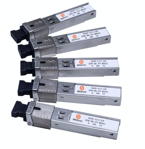
14Gbps850nm SFP+ Transceiver,100m Reach storage module
SOSP-8596-01
1.Applications
Ø Tri-Rate 14.025 Gb/s Fibre Channel
Ø Other optical links
2.Features
Ø Up to 14.025 Gb/s bi-directional data links
Ø Hot-pluggable SFP+ footprint
Ø Built-in digital diagnosticfunctions
Ø Built-in CDR with shut offcontrol
Ø 850nm Oxide VCSEL lasertransmitter
Ø Duplex LC connector
Ø RoHS compliant and Lead Free
Ø 35m on 50/125um MMF
Ø 100m on high-bandwidth 50/125um(OM3)
Ø Metal enclosure, for lower EMI
Ø Single 3.3V power supply
Ø Operating temperature range:0°C to 70°C
3. Description
Sinovo’s 16G SW SFP+ transceivers are designed for use in Fibre Channel links up to14.025
Gb/s data rateover multimode fiber. They are compliantwith FC-PI-5 Rev. 6.00a, SFF-8472 Rev 11.0c and SFF-8081h, andcompatible with SFF-8432b and applicable portions of SFF-8431 Rev. 4.1d.The opticaltransceiver is compliant per the RoHS.
4.standard
Ø Electrical interface compliant toSFF-8431
Ø Compliant with SFF-8472 Rev 10.2
Ø Compliant with IEEE 802.3ae10GBASE-LR and 10GBASE-LW
Ø RoHS Compliant
5.Performance Specifications
5.1.Absolute Maximum Ratings
These values represent the damage threshold of the module. Stress inexcess of any of the individual Absolute Maximum Ratings can cause immediatecatastrophic damage to the module even if all other parameters are withinRecommended Operating Conditions.
Table.1 Absolute maximumratings
ParameterSymbolMinMaxUnit
Maximum Supply VoltageVcc-0.54.0V
Storage TemperatureTs070°C
RX Input Average PowerPmax 0dBm
Relative HumidityRH585%
5.2.Recommended Operating Conditions
Table.2 RecommendedOperating Conditions
ParameterSymbolMinTypicalMaxUnit
Operating Case TemperatureStandard Tc02570°C
Power Supply VoltageVcc3.153.33.46V
Power Supply CurrentIcc 290mA
Power DissipationPD90 800mW
Data RateDR 14.025 Gbps
Transmission DistanceTD 100 m
5.3. Transmitter Specification
Table.3 TransmitterSpecification (Optical)
ParameterSymbolMin.Typ.Max.UnitNote
Average Output PowerPo-7.8 dBm
Disable PowerPoff -40dBm
Extinction RatioER3.5 dB
Output Centre Wavelengthλc840 860nm
Spectral Width (RMS) @ 14.025Gb/sΔλ 0.59nm
Optical Modulation Amplitude @ 14.025 Gb/sOMA-4.8 dBm
Optical Return LossORL -12dB
Transmitter Waveform and Dispersion PenaltyDP 4.3dB
Optical Rise/Fall Time
(20%~80%)@
tr/tf 0.09ns
Optical Eye MaskMMCompliant to IEEE802.3ae1
Relative Intensity NoiseRin -128(12dB reflection)dB/Hz
Note: 1. Measured at 14.025Gbps, PRBS2^31-1, NRZ
Table.4 TransmitterSpecification (Electrical)
ParameterSymbolMinTypicalMaxUnit
Data Input Swing DifferentialVIN90 800mV
Input Differential ImpedanceZIN90100110Ω
Transmit Disable InputHighVIH2.0 Vcc+0.3V
LowVIL0 0.8V
Transmit Enable OutputHighVOHVee Vee+0.8V
LowVOL0 0.4V
5.4. Receiver Specification
Table.5 ReceiverSpecification (Optical)
ParameterSymbolMinTypicalMaxUnitnote
Centre Wavelengthλc840850860nm
Receiver SensitivitySen -10.5dBm2
Receiver OverloadPsat0 dBm2
LOS De-AssertLOSD -13dBm
LOS AssertLOSA-30 dBm
LOS Hysteresis 0.5 dB
Receiver ReflectanceRrx -12dB
Note :2. Measured at BER10-12, 14.025Gbps, PRBS2^31-1, NRZ
Table.6 ReceiverSpecification (Electrical)
ParameterSymbolMinTypicalMaxUnitnote
Data Output Swing DifferentialVout185 425mV
Deterministic Jitter @ 14.025 Gb/sRX DJ 0.22UI
LOS OutputHighVOH2 Vcc+0.3V
LowVOLVee Vee+0.8V
5.5. Diagnostics Specification
Table.7Diagnostics Specification
ParameterRangeUnitAccuracyCalibration
Temperature0 to 70℃±3℃Internal / External
Voltage3.0 to 3.6V±3%Internal / External
Bias Current0 to 100mA±10%Internal / External
TX Power-7.8 to 0dBm±3dBInternal / External
RX Power-30 to 0dBm±3dBInternal / External
5.6. Pin Definitions
Table.8Pin Definitions
PINSymbolDescriptionRemarks
1VEETTransmitter ground (common with receiver ground)Circuit ground is isolated from chassis ground
2Tx_FaultTransmitter Fault. Not supported
3Tx_DisableTransmitter Disable. Laser output disable on high or openDisabled: TDIS>2V or open
Enabled: TDIS<0.8V
4SDA2-wire Serial Interface Data LineShould Be pulled up with 4.7k – 10k ohm on host board to a voltage between 2V and 3.6V
5SCL2-wire Serial Interface Clock Line
6MOD_ABSModule Absent. Grounded within the module.
7RS0No connection required
8RX_LOSLoss of Signal indication. Logic 0 indicates normal operationLOS is open collector output
9RS1No connection required
10VEERReceiver ground (common with transmitter ground)Circuit ground is isolated from chassis ground
11VEERReceiver ground (common with transmitter ground)
12RD–Receiver Inverted DATA out. AC coupled
13RD+Receiver Non-inverted DATA out. AC coupled
14VEERReceiver ground (common with transmitter ground)Circuit ground is isolated from chassis ground
15VCCRReceiver power supply
16VCCTTransmitter power supply
17VEETTransmitter ground (common with receiver ground)Circuit ground is isolated from chassis ground
18TD+Transmitter Non-Inverted DATA in. AC coupled
19TD–Transmitter Inverted DATA in. AC coupled
20VEETTransmitter ground (common with receiver ground)Circuit ground is isolated from chassis ground
5.7. Timing Electrical Interface
Table.9 Timing ElectricalInterface
ParameterSymbolMinMaxUnitsConditions
Tx_Disable Assert Timet_off 100usRising edge of Tx_Disable to fall of output signal below 10% of nominal
Tx_Disable Negate Timet_on 2msTx_Disable negate time. Falling edge of Tx_Disable to rise of output signal above 90% of nominal. This only applies in normal operation, not during start up or fault recovery.
Time to initialize t_start_up 300msFrom power supplies or hot plug or Tx disable negated during power up, or Tx_Fault recovery, until non-cooled power level I is fully operational.
Tx_Fault Assert TimeTx_Fault 1msFrom occurrence of fault to assertion of Tx_Fault
Tx_Fault to Resett_reset10 usTime Tx_Disable must be held high to reset Tx_Fault
Rx_LOS Assert Timet_los_on 100usFrom occurrence of loss of signal to assertion of Rx_LOS
Rx_LOS De-Assert Timet_los_off 100usFrom occurrence of presence of signal to negation of Rx_LOS
5.8. Mechanical Dimensions
Diagram of Mechanical Dimensions
6.Aplication Cautions
6.1.ESD
Thistransceiver is specified as ESD threshold 1kV for high speed pins and 2kV forall other electrical input pins, tested per MIL-STD-883, Method 3015.4/JESD22-A114-A (HBM). However, normalESD precautions are still required during the handling of this module. Thistransceiver is shipped in ESD protective packaging. It should be removed fromthe packaging and handled only in an ESD protected environment.
6.2. LASER SAFTY
This is aClass 1 Laser Product according to IEC 60825-1:1993:+A1:1997+A2:2001. This product complies with 21 CFR 1040.10 and1040.11 except for deviations pursuant to Laser Notice No. 50, dated (July 26,2001)
Contact :
Address11/F,Taibang Technology Building,Gaoxin South 4th,Science and Technology Park South,Nanshan,Shenzhen,China
Zip518040
Tel+86(0)0755-3295 9919
Fax+86(0)755 3295 9918
Websitewww.sinovocorp.com
